Adv. Radio Sci., 8, 129–133, 2010 www.adv-radio-sci.net/8/129/2010/ doi:10.5194/ars-8-129-2010
© Author(s) 2010. CC Attribution 3.0 License.
Advances in
Radio Science
Noise of short-time integrators for readout of uncooled infrared
bolometer arrays
D. W ¨urfel, D. Weiler, B. J. Hosticka, and H. Vogt
Fraunhofer Institute for Microelectronic Circuits and Systems, Duisburg, Germany
Abstract. As state-of-the-art readout circuits short-time in-tegrators in Far Infrared (FIR) uncooled bolometer arrays are commonly used. This paper compares the transfer functions of an ideal continuous-time integrator with that of a real inte-grator with focus an OTA parameters and noise analysis. Be-side the noise sources at the non-inverting input of the OTA special care has to be taken to account for capacitances at the inverting input. The Noise Equivalent Temperature Dif-ference (NETD) as the key parameter for bolometer applica-tions for a real short-time integrator will be derived. As the result it will be shown, that the NETD is 1/f-noise limited.
1 Introduction
The need for uncooled infrared focal plane arrays (IRFPA) for imaging systems has increased since the beginning of the nineties. Examples for the application of IRFPAs are ther-mography, pedestrian detection for automotive, firefighting and infrared spectroscopy. According to Plank’s law, each body with a temperature above absolute zero point emits electro-magnetic radiation. The wavelength and intensity de-pends on the temperature of the body. For example, a body at a temperature of 300 K has its maximum emittance at a wave-length of approx. 10 µm. FIR imager uses the IR-radiation of a warm body in the wavelength range between 8..14 µm. The FIR-sensitive element is the bolometer which changes its resistance by absorbing the radiation of the warm body. A pulsed bias with a constant voltage is applied to the bolome-ter and the resulting current is integrated for a fixed time. An offset current is subtracted before integration. Conventional readout circuits use a column-wise architecture.
Correspondence to: D. W¨urfel
2 Bolometer
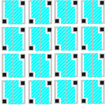
The bolometer is fabricated by post-processing on CMOS wafers in Fraunhofer IMS Microsystem Lab. The realization of a microbolometer is shown in Fig. 1 as a cross section. A micromachined membrane consisting of amorphous silicon is suspended by two via stacks of metal from the CMOS sub-strate. The membrane forms with two other layers a good interferometric structure for radiation absorption. On top of the membrane an antireflection layer with a sheet resistance of 377/sq is deposited. The bottom structure consists of a nearly perfect reflecting metal layer (Ruß et al., 2007). To increase the thermal resistance the membrane is fixed by two small legs (Fig. 2). The optical distance between membrane and reflection metal reaches an optimum for one quarter of the radiation wavelength. To reduce thermal losses by gas conduction a vacuum package is required. The bolometer converts the infrared radiation into heat energy and this in-duces a temperature rise resulting in a change of the electri-cal resistance. Typielectri-cal bolometers have pixel pitch values of 35 µm or 25 µm. Figure 2 shows a bolometer array with 4×4 sensor elements.
3 Short-time integrator
In Sect. 1, the ideal integrator model is analysed. In Sect. 2, the real integrator circuit is presented, analysed and com-pared to the ideal model.
3.1 Ideal model
Figure 3 shows the ideal short-time integrator model in the time-domain. By applying a bias voltage pulse vBias(t )=
VBiasto the bolometer resistorRBolo(T0)the bolometer cur-rentiBolo(t )is generated and integrated at the integration ca-pacitorCint. Only a small part of the bolometer current de-pends on the IR-radiation, so a bias currentiBias(t )=IBiasis
130 D. W¨urfel et al.: Noise of short-time integrators
11
Figure 1.
Realization of a bolometer (cross section)
Figure 2.
Layout of a bolometer array
Σ
tPixel
+
-vBias(t)
RBolo(T0)
1 +
-iBias(t)
22 Cint
vout(t) -1
∫
Σ
iBolo(t)
Figure 3.
Ideal integrator-model
Fig. 1. Realization of a bolometer (cross section).subtracted at the first summation node in order to cancel a corresponding offset at the integrator output. The integration stops after readout timetPixel. This is modelled in the follow-ing way: the second summation node subtracts the replica of the bolometer current delayed by the readout timetPixel and integrates it. The integration constant is−1/Cint. In this way we obtain a “time-windowed” integration. Otherwise the ideal integration would never end. The output voltage
Vout(s)is calculated in the Laplace-domain in Eq. (1).
Vout(s)= 1−e−stPixel −1
sCint U
Bias(s)
RBolo(T0)
−IBias(s)
(1) Thus the transfer functions for output voltageVout(s)over input voltageVBias(s)and input currentIBias(s)are given by Eqs. (2) and (3).
Hin,ideal(s)=
Vout(s)
VBias(s)
= 1−e−stPixel −1
sRBolo(T0)Cint (2)
Hin2,ideal(s)=
Vout(s)
IBias(s)
= 1−e−stPixel −1
sCint
(3)
3.2 Real integrator
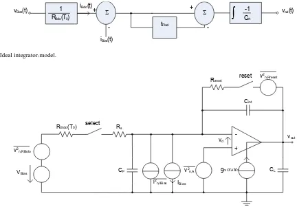
Figure 4 shows the real readout integrated circuit (ROIC) consisting of an OTA with an integration capacitor Cint in the feedback and all relevant noise sources. The output re-sistance is assumed to be infinity. The single-stage OTA is compensated by a load capacitanceCL. The integrator is
re-seted by the switch “reset”. A parasitic capacitorCpcaused
e.g. by a column line is placed at the inverting input of the OTA. After the reset phase bolometer and a current source are connected to the inverting OTA input by the switch “se-lect” for the readout timetPixel. The current from the cur-rent source is a constant during the integration, but there is no current if the switch “select” is off. Then the output voltage is held and sampled by a following stage not shown here. The switch resistanceRs in series with the
bolome-ter resistorRBolo(T0)can be neglected, becauseRBolo(T0)
Rs. If the transconductance of the OTA is sufficiently high,
so thatgmOTARBolo(T0)1 andCintgmOTARBolo(T0)CL,
the output voltageVout(s)is given by
11
Figure 1. Realization of a bolometer (cross section)
Figure 2. Layout of a bolometer array
Σ
tPixel
+
-vBias(t)
RBolo(T0)
1 +
-iBias(t)
22 Cint
vout(t)
-1
∫
Σ
iBolo(t)
Figure 3. Ideal integrator-model
Fig. 2. Layout of a bolometer array.Vout(s)= 1−e−stPixel·
Vn,A(s)1+s Cint+CpRBolo(T0)+(IBias(s)RBolo(T0)−VBias(s))
1−sCint
gmOTA
sCintRBolo(T0)
1+ sCe
gmOTA
(4) with
Ce=CL+Cp+
CLCp
Cint
. (5)
From Eq. (4) 3 transfer functions can be derived:
Hin1(s)=
Vout(s)
VBias(s)
=
−1− sCint gmOTA
sCintRBolo(T0)
1+ sCe gmOTA
1−e
−stPixel (6)
Hin2(s)=
Vout(s)
IBias(s) =
1− sCint gmOTA
sCint
1+ sCe gmOTA
1−e
−stPixel (7)
Hin3(s)=
Vout(s)
Vn,A(s)
=
1
sCintRBolo(T0)
+1+ Cp
Cint 1
1+ sCe gmOTA
1−e−stPixel (8)
Hin1(s) and Hin2(s) compared to Hin1,ideal(s) and
Hin2,deal(s), respectively, shows that there is now a zero in the transfer function and an additional non-dominant pole, which is given by the gain bandwith product (GBW) of the OTA. If the zero is not dominant, its effect can be
D. W¨urfel et al.: Noise of short-time integrators 131
11
Figure 1.
Realization of a bolometer (cross section)
Figure 2.
Layout of a bolometer array
Σ
tPixel
+
-vBias(t)
RBolo(T0)
1 +
-iBias(t)
22 Cint
vout(t) -1
∫
Σ
iBolo(t)
Figure 3.
Ideal integrator-model
Fig. 3. Ideal integrator-model.Cint
+ -RBolo(T0)
CL Cp
VBias gmOTAvd
vd vout Rs
select
IBias
Rreset reset
v2 n,A v2
n,RBolo
i2 n,IBias
v2 n,Rreset
Figure 4.
Real ROIC with an OTA (noise sources included)
Fig. 4. Real ROIC with an OTA (noise sources included).neglected. But Hin3(s)is of special interest. Noise at the noninverting input of the OTA is integrated but additionally amplified by(1+Cp/Cint)up to the GBW. There could be a high amplification if there is a large parasitic capacitance and a small integration capacitance with a large bandwith dependent on OTA’s GBW.
4 Noise calculation and NETD
The power noise density SRBolo including white and 1/f
-noise for the bolometer resistor is given by
SRBolo(f )=
v2n,RBolo,w
1f +
vn,2RBolo,1/f
1f
=4kT0RBolo(T0)+VBias2
kfBolo
f (9)
withkas Boltzman’s constant,kfBolothe 1/f-noise parameter andT0as the reference temperature. The power noise density
SAincluding white and 1/f-noise for the OTA is given by
SA(f )=
vn,A,w2
1f +
v2n,A,1/f
1f
=24KakT0nγ
gmOTA
+2Kb
kfOTA
W LC2
oxf
(10)
withW as the width of the input transistor,Las the length of the input transistor,Cox as the capacitance per unit of the
transistor, n the weak inversion slope parameter, γ as the noise parameter andkfOTAas the 1/f-noise parameter of the input transistor (Anelli, 2000). Ka andKb account for the
effect of OTA’s remaining transistors on total OTA’s white noise and 1/f-noise respectively. The power noise density of the current source depends on the realization. In the simplest case it could be a resistor with the same resistance as the bolometer resistance. To make it easy it is assumed that the current source is ideal, but has a power noise density given by
SIBias=
in,2IBias,w
1f =
4kT0
RBolo(T0)
. (11)
At first the noise power at the integrator output caused by the bolometer for white noise is calculated.
132 D. W¨urfel et al.: Noise of short-time integrators
vn,2out,RBolo,w=
∞
Z
f=0H z
v2n,Bolo,w
1f |Hin1(f )|
2df=
∞
Z
f=0H z
4kT0RBolo(T0)
2sin(πf t
Pixel) 2πf RBolo(T0)Cint
2
· 1
1+2πf Ce gmOTA
2df+
∞
Z
f=0H z
4kT0RBolo(T0)
2sin(πf t
Pixel) 2πf RBolo(T0)Cint
2 ·
2πf Cint gmOTA
2
1+2πf Ce gmOTA
2df
≈
∞
Z
f=0H z
4kT0RBolo(T0)
2sin(πf t
Pixel) 2πf RBolo(T0)Cint
2
df+
∞
Z
f=0H z
4kT0RBolo(T0)
2
2πf RBolo(T0)Cint 2
·
2πf Cint gmOTA
2
1+2πf Ce gmOTA
2df
≈2kT0
tPixel
RBolo(T0)Cint2
+ 2
gmOTARBolo(T0)Ce
!
(12)
This result has been obtained using several approximations. The noise power at the output caused by the current source is calculated similarly as:
vn,2out,IBias,w=
∞
R
f=0H z i2
n,IBias,w
1f |Hin2(f )|
2df≈2kT 0
tPixel RBolo(T0)C2int
+ 2
gmOTARBolo(T0)Ce
. (13)
The noise power caused by OTA’s white noise is determined as
vn,2out,A,w=
∞
Z
f=0H z
vn,A,w2
1f |Hin3(f )|
2df≈
∞
Z
f=0H z
24KakT0nγ
gmOTA
1
RBolo(T0)Cint
·2sin(πf tPixel) 2πf
2 +2
1+CP
Cint 2
1+2πf Ce gmOTA
2 df
≈4KakT0nγ
gmOTA
tPixel
(RBolo(T0)Cint)2 +2
1+CP
Cint 22K
akT0nγ
Ce
.
(14) The noise power caused by the bolometer resistor’s 1/f-noise is described as
vn,2out,RBolo,1/f =
∞
Z
f1
v2n,Bolo,1/f
1f |Hin1(f )|
2df=
∞
Z
f1
VBias2 kfBolo f
1
RBolo(T0)Cint
·2sin(πf tPixel) 2πf
2
· 1
1+
2πf Ce gmOTA
2df+
∞
Z
f1
VBias2 kfBolo f
1
RBolo(T0)Cint
·2sin(πf tPixel) 2πf
2 ·
2πf Cint gmOTA
2
1+2πf Ce gmOTA
2df
≈VBias2 kfBolo(−1)
−1+cos(ξ )−ξsin(ξ )+ξ2Ci(ξ ) ξ2R2
Bolo(T0)Cint2
tpixel2 + V 2 BiaskfBolo
(gmOTARBolo(T0))2 ln r
1+2πf1gmOTACe 2
2πf1gmOTACe
≈VBias2 kfBolo
tPixel
RBolo(T0)Cint 2
ln 1
2πf1tPixel
+ 1
(gmOTARBolo(T0))2 ln
1
2πf1gCe mOTA
.
(15) where ξ = 2π tPixelf1, cos(ξ ) ≈ 1, sin(ξ )≈ ξ, the
Cosine Integral Ci(ξ ) ≈ln(ξ ) with |ln(ξ )| 1 and 2πf1Ce/gmOTA 1. A mechanical shutter in front of the IRFPA is periodically closed. This can be modelled as a high
pass filter. The lower frequencyf1is assumed to be (Wood, 1997)
f1≈ 1 4tshutter
. (16)
D. W¨urfel et al.: Noise of short-time integrators 133
tshutteris the shutter time, wheretshuttertPixel. The contribu-tion of the 1/f-noise of the OTA with same approximations as above is given by
vn,2out,A,1/f =
∞
R
f1 v2n,A,1/f
1f |Hin3(f )|
2df
≈
∞
R
f1
2KbW LCkfOTA2 oxf
(2sin(πf tPixel))2 (2πf RBolo(T0)Cint)2
+ +1+CP
Cint 2
4
1+2πfgCe mOTA
2
df
≈2KbW LCkfOTA2 ox
tPixel RBolo(T0)Cint
2
ln2π t1 Pixelf1
+ 41+CP
Cint 2
ln 1
2πf1gmOTACe
!
.
(17)
During the reset of the integrator the kTC-noise is stored on the integration capacitor. Thus
vn,2reset=kT0
Cint
. (18)
The current responsitivity of the bolometer at the input is given for a constant voltage across the bolometer by
RI≈
−VBiasα
RBolo(T0)gBolo
. (19)
whereα is the temperature coefficient (TCR) and gBolo is the heat conductance of the bolometer (derived from Wood, 1997) withgBolo≈geff,IBolo=VBias/RBolo(T0),α <0,IBolo as the constant bolometer current,geff as the effective heat conductance). The TCRαis assumed to be constant. The total output noise power is refered to the input by mul-tiplying by the square of the DC value of the transfer-functionHin1(f )and converted into a current by division by
RBolo2 (T0). The NETD is defined as
NETD= 4·F
2
no
π·ABolo·εBolo·dTdL target
q
in,2total
RI
(20) wherein,totalis the total noise current,Fnois the f-number of
the optic,ABolothe area of the bolometer,εBolois the emis-sion coefficient which is equal to the absorption coefficient anddL/dTtarget is the differential change of radiance over the change of the target temperature (Wood, 1997). Finally, total NETD is calculated to
NETD= 4·Fno2 π·ABolo·εBolo·dTtdLarget
· 1
RBolo(T0)
·RBolo(T0)Cint tPixel
·
· v u u t
v2n,out,RBolo,w+v2n,out,RBolo,1/f+vn,2reset
+vn,2out,IBias,w+vn,2out,A,w+vn,2out,A,1/f
!
RI
(21)
Assuming that there is only noise from the bolometer resistor (white and 1/f-noise) and current source (white noise) with
gmOTA→ ∞,CL→ ∞, WL→ ∞the NETD reaches
NETD= 4·Fno2gBolo π·ABolo·εBolo·dTtdLarget
· r
4kT0RBolo(T0)
tPixel +VBias2 kfBololn 2tshutter
π tPixel
|−VBiasα| . (22) NETD caused by white noise can be decreased by increas-ing the readout time and bias voltage and by decreasincreas-ing the bolometer resistance assuming that the bolometer parameters and f-number are fixed. NETD caused by 1/f-noise is inde-pendent of the bias voltage, because it cancels out. Because of the logarithm there won’t be much change when varying
tPixel for a fixed shutter time. Thus white noise can be re-duced, but 1/f-noise cannot. So 1/f-noise will limit NETD.
5 Conclusions
The ideal and real short-time integrator have been modelled. The effect of the finite integration time has been included. The total noise power and the resulting NETD have been calculated. For long integration the limiting factor as far as NETD is concerned is 1/f-noise.
References
Ruß, M., Bauer, J., and Vogt, H.: The geometric design of mi-crobolometer elements for uncooled focal plane arrays, Proc. of SPIE Conference Infrared Technology and Applications XXXIII, Volume 6542, 654223–1–10, 2007.
Anelli, G.: Design and Characterization of Radiation Tolerant Inte-grated Circuits in Deep Submicron CMOS Technologies for the LHC Experiments, Ph.D. Thesis, Institut National Polytechnique de Grenoble, France, 2000.
Wood, R. A.: Monolithic Silicon Microbolometer Arrays, in Un-cooled Infrared Imaging Arrays and Systems, edited by: Kruse, P. and Skatrud, D., Semiconductors and Semimetals, 47, 45–121, Academic Press, 1997.