Reproducing system-level bulk current injection test in direct power
injection setup for multiple-port DUTs
S. Miropolsky and S. Frei
TU Dortmund, Dortmund, Germany
Correspondence to: S. Miropolsky ([email protected])
Abstract. Many investigations have been published on the transferability of RF immunity test results between system and IC-levels. The RF signal level at DUT (Device under Test) inputs, i.e. either RF voltage amplitude or RF input cur-rent, is used as a reference value for the load on the DUT. Ex-isting approaches analyze the DUT response as a function of the RF signal level at a single input pin, e.g. supply voltage. Sufficient accuracy of such an approach could be shown in several cases, but results are not sufficient as a general solu-tion for complex DUT. This paper proposes both theoretical analysis and practical implementation of a DPI setup, where a disturbance, equivalent to system-level BCI setup, can be delivered to multiple DUT input ports.
1 Introduction
Among the main trends of today’s electronic industry, the safety and reliability, and in particular the EMC is of higher importance. The devices are tested for both EM interference (EMI) and susceptibility (EMS). The Direct Power Injec-tion (DPI, IEC, 2006) is a common method for IC testing, while at system-level various methods, e.g. Bulk Current In-jection (BCI, ISO, 2005) or Absorber Line Shielded Enclo-sure, (ALSE), are used.
A system-level EMC test requires large and complex test setups with cable harnesses and special RF equipment, and thus can only be performed in specialized EMC laboratories, while the DPI test can be more easily performed in a com-mon test laboratory. Multiple investigations have been pub-lished to find the correlation between system- and IC-level tests. Simulation models for BCI setups are developed since at least 1986 (Sultan, 1986), and the investigations continue up to now (Grassi et al., 2007; Lafon et al., 2007; Alaeldine et al., 2007; Miropolsky et al., 2011). The theory of common into differential mode RF signal conversion at the test PCBs
is actively discussed e.g. in Crovetti and Fiori (2011). The RF signal level at the DUT pins is proposed to be a reference value for comparative analysis of test results (Miropolsky and Frei, 2011; Oguri and Ichikawa, 2012). Several propos-als have been made to calculate the equivalent DPI forward power necessary to produce the same RF signal at DUT as in the original BCI test (Miropolsky and Frei, 2011; Durier et al., 2011). The test results are either compared using the equivalent DPI power level, or the calculated equivalent for-ward power is injected into the DUT in the DPI setup and the DUT response is compared to that of the BCI test. The sum-marized goal of these investigations is to find a method to test the ICs so that the success of the consequent system-level RF immunity test is assured.
Existing approaches analyze the DUT response as a func-tion of the RF signal at a single input pin, e.g. at supply pin. High accuracy could be observed in several cases (Miropol-sky and Frei, 2011; Durier at al., 2011; Oguri and Ichikawa, 2012), but this cannot be applied as a general solution. In case of BCI test of two-pin modules reproducing the differ-ential RF disturbance at a single pin pair (supply vs. ground) is sufficient. However, in case of three pin sensors (Durier at al., 2011; Oguri and Ichikawa, 2012), where signal and sup-ply lines are separate, the RF signal coupled to a supsup-ply line might influence the immunity threshold at a signal pin and vice versa. In a BCI test on a CAN or FlexRay transceiver network both common and differential RF signals at the two IC pins can be responsible for an IC failure. Thus in the dis-cussion of equivalent conversions the RF injection into mul-tiple pins has to be considered.
178 S. Miropolsky and S. Frei: Reproducing system-level BCI test in DPI setup
Fig. 1. Sample BCI test setup structure and overview.
Fig. 2. Sample BCI test setup simulation circuit.
This paper proposes a DPI testing method, where the RF disturbances, equivalent to an original BCI setup, can be de-livered to multiple DUT pins.
2 Sample study case:
a system-level Bulk current injection setup 2.1 Test setup structure and overview
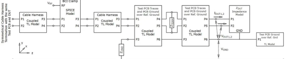
The system level test setups usually contain of one or more electronic control units (ECU, here called EUT), connected to each other or to the support circuitry with a cable har-ness. A sample system discussed in current paper consists of two CAN transceiver units. Each EUT is a small PCB con-taining the transceiver IC (DUT) with necessary periphery, e.g. bus terminations of 120, traces, ports, supply voltage protection, etc. These EUT PCBs are located in 5 cm over the reference ground plane. Depending on the application the PCBs may optionally be grounded to the main reference ground with a low impedance connection (e.g. metal tape). The EUTs are connected to each other with a twisted pair ca-ble of 1 m length in 5 cm above the taca-ble. The transceivers communicate over this cable. The RF disturbance of spec-ified amplitude is injected into the cable harness using one of the mentioned methods, and safe operation of the system under RF disturbance should be assured.
Theoretically, any RF immunity test method can be used for such network. In the current work the BCI method is con-sidered, and the setup shown in Fig. 1 is discussed. The BCI injection clamp is placed at a specified position along the ca-ble harness.
According to the method (BCI, ISO, 2005), the BCI clamp has to be calibrated in advance, and the forward power neces-sary to inject a certain common mode current amplitude into the cable harness must be measured. To simplify the anal-ysis, this step is avoided and constant forward power level is injected. For real application, the calibration curve of the BCI clamp has to be considered. This however can be intro-duced by just another scaling coefficient in the calculation procedure.
According to a general assumption supported by many au-thors (Miropolsky and Frei, 2011; Durier at al., 2011; Oguri and Ichikawa, 2012), the DUT response is dependent on the RF signal delivered through the test setup to the IC pins. The test setup is no more than a small-signal transfer function from the system RF port to the DUTs. To obtain the transfer function a small-signal model of the setup is necessary. 2.2 Small-signal simulation model
The simulation model shown in Fig. 2 is assembled accord-ing to the original setup.
The FCC F140 BCI clamp is modelled with a circuit simi-lar to one shown in Miropolsky and Frei (2011). The twisted cable harness is modelled as lossy coupled transmission line (TL). The cable parameters were obtained by analyzing the cable cross-section with HSPICE 2-D field solver. The twist-edness effect is neglected in the model for simplicity pur-poses.
10
104
105
106
107
108
109
10 20 30 40 50 60 70 80 90
Frequency, Hz
Im
p
ed
an
ce
,
d
B
ZPIN1 VNA Measurement ZPIN2 VNA Measurement ZPIN1 Approximated Model ZPIN2 Approximated Model
5
Figure 3. Sample DUT input impedances, measurement and macro-model 6
7
Figure 4. One-port equivalent RF source 8
Fig. 3. Sample DUT input impedances, measurement and
macro-model.
traces are study-case-dependent, and thus are irrelevant for the general discussion purpose.
The 120CAN bus termination is modeled as simple re-sistor (ZT ERM)in the middle between the PCB input ports
and DUT (see Fig. 2). Since the DUT is located in the cen-ter of the test PCB, the remaining PCB ground plane pro-vides additional coupling to the reference ground, this effect is considered with one more TL device.
The model is used to simulate RF signal levels at DUT pins in the BCI test. These levels are used as a reference to generate and verify the equivalent DPI setup.
2.3 DUT input impedance
The DUT impedance can often be modeled as a RC circuit, with additional package effects visible at higher frequencies. Commonly the impedances may be considered to be close to RC up to approx. 100 MHz. More complex models have to be considered above this frequency.
In the analysis of multiple-port DUTs, under the assump-tion of possible internal coupling between the pins, repre-senting DUT as a set of pin-to-ground impedances is insuffi-cient. A full port-to-port impedance matrix must be consid-ered.
In current work a sample CAN transceiver IC is analyzed as example DUT. The RF injection into differential inter-face consisting of two pins, CANH and CANL, is consid-ered. A linear impedance model is created as a numerical ap-proximation of measurement data. The two-port impedance dataset is captured with VNA and deembedded with the Mat-lab RF Toolbox. The data is approximated with vector fitting (Gustavsen and Semlyen, 1999 ), and an equivalent SPICE model for the approximation is generated. The impedances are shown in Fig. 3.
3 Equivalent DPI source calculation procedure 3.1 Motivation
The development of an equivalent DPI test follows a single goal: the RF disturbances that appear in the complex
system-Fig. 4. One-port equivalent RF source.
level setups, e.g. BCI, should be reproduced in a simplified low-cost DPI setup. Among the initial conditions we must note the fixed 50impedance of RF sources, and significant limitations on reproducing arbitrary impedances in physical setups. On the other side significant freedom degree is avail-able in controlling RF amplitudes and phase shifts of several 50sources.
3.2 Equivalent DPI source calculation
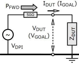
According to (Durier at al., 2011), the equivalent DPI power level can be calculated with a commercial calculator from the complex RF voltage and current values, which must be extracted from system level setup simulation or measurement as a table vs. frequency. This implies the known value of the DUT input impedance. In this case the internal RF amplitude of the source can be simply calculated at each frequency with Eq. (1).
VDPI=VGOAL+R50·IGOAL (1)
PDPI=VDPI2 /4R50 (2)
The procedure is illustrated in Fig. 4. The index “GOAL” refers to the signal to be reproduced at RF source output. The equivalent DPI source level is valid only for current DUT impedance. Attaching another DUT to the setup results in different RF signal values at DUT ports, and another calcu-lation of an equivalent DPI source is necessary. This is a sig-nificant disadvantage comparing to e.g. an equivalent Norton source, since the latter generates the signal at the load in strict correlation to original setup for any load impedance.
180 S. Miropolsky and S. Frei: Reproducing system-level BCI test in DPI setup
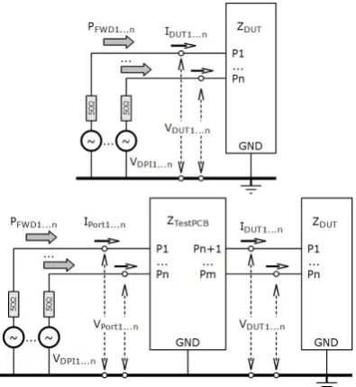
Fig. 5. Multiple-port equivalent DPI RF source (a) direct injection
into DUT (virtual case) (b) accounting for the PCB transfer function (realistic case).
An example of an equivalent setup for a single two-port DUT is shown in Fig. 5a.
3.3 DPI PCB properties
In physical DPI test the RF source is never connected to the DUT directly, but to the RF port of the test PCB. The transfer function from the PCB RF port to the DUT pins must be considered. Since the DPI test is performed on a grounded PCB, only the differential signal transfer must be considered, the PCB ground plane is used as the signal reference.
The easiest approach to introduce the transfer function is to use a multiport ABCD matrix of the PCB structure (3):
VPORT
IPORT
=
APCB BPCB CPCB DPCB
·
VDUT
IDUT
(3) whereV andI are vectors of differential voltages and cur-rents, i.e. with PCB ground plane used as a reference. The indices correspond to signals at DUT pins (VDUT,IDUT)and signals at PCB ports at cable harness side (VPORT,IPORT), as shown in Fig. 5b. Each A, B, C and D element is a sub-matrix with a size corresponding to the number of ports at each PCB side. The sub-matrices can be found by solving the linear equation system of the admittance representation (Eq. 4) for vectorsVPORTandIPORT.
IPORT
IDUT
=
YPCB
·
VPORT
VDUT
(4) The values of the equivalent DPI sources (VDPI)can then be calculated with Eqs. (1) and (2) using RF signals at PCB ports (VPORT andIPORT)as “goal” values. When the 50
Fig. 6. Equivalent DPI test setup for sample two-port DUT,
overview.
RF sources with calculated amplitude and phase are attached to the PCB ports, the RF signals VDUT and IDUT will be reproduced at DUT pins.
The impedance matrix of the test PCB can be obtained by either passive modeling approach with discrete circuit ele-ments or with e.g. 3-D EM field simulations or with VNA measurements.
4 Equivalent DPI source application
The general procedure for equivalent DPI source develop-ment is described in Sect. 3. In the current application, the “original” RF signal levels at DUT (VDUT1,2,IDUT1,2)are obtained by AC simulation of a BCI setup model discussed in Sect. 2.2 with DUT impedances discussed in Sect. 2.3. 4.1 Single-DUT testing with equivalent DPI source The same test PCB as in BCI test can be used. The RF ports are connected between the PCB traces and ground as shown in Fig. 6. The PCB model is developed in a similar way as for the main BCI test setup. The ABCD-matrix of the PCB is calculated. The test PCB port signals (VPORTandIPORT)are calculated with Eq. (3). The RF source amplitude is calcu-lated with Eq. (1) using port signals as goal values. Attaching the RF sources to PCB ports will reproduce the original RF signal levels at DUT (VDUT1,2,IDUT1,2), both in simulation and, more important, in measurement. The resulting circuit is the same as shown in Fig. 5b.
The single-DUT configuration can be efficiently used for other DUT types, e.g. sensor ICs. In the case discussed here at least two ICs are necessary to establish the communica-tion. A two-DUT configuration must be considered.
4.2 Two-DUT equivalent DPI configuration
Fig. 8. Equivalent DPI test setup for two sample two-port DUTs, simulation.
From the RF source point of view, the two test PCBs are just the loads connected in parallel, thus the RF sources ampli-tudes can be calculated with Eq. (1) usingVPORT1,2voltages and doubleIPORT1,2currents as “goal” values.
Obviously, in the real BCI test such symmetry cannot be expected. Different RF signals have to be reproduced at both DUTs. Theoretically, it can be performed with a 4-port equiv-alent RF source of the same or similar structure. However, in real application such configuration is rather unrealistic. Each physical RF source consists of a signal generator followed by an amplifier. Equivalent DPI implies the control of both amplitude and phase. Hence the complexity of such configu-ration with four physical sources is very high, and running a BCI test would be more effective.
To avoid unnecessary complexity, the RF levels of each DUT in the BCI setup can be reproduced sequentially. The first set of equivalent RF sources is calculated to reproduce the original RF levelsVDUT1,2andIDUT1,2at both DUTs. The same procedure is performed for the second set of RF signals
VDUT3,4andVDUT3,4. This way after two test iterations each of the DUT ICs is subdued once to a RF disturbance equiva-lent to that from the BCI test.
4.3 Simulation results
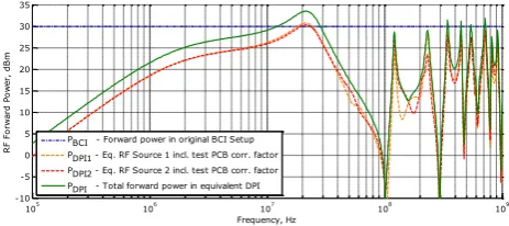
The calculated forward power levels (PDPI) is shown in Fig. 9. Generally, the equivalent source forward power is much lower than the original forward power injected into the BCI setup, i.e. only a small part of the produced RF power is delivered to the DUTs. However, at resonance locations the values reach and even exceed the original BCI forward power. Since the two sources are injecting RF signals simul-taneously, the total forward power is even higher.
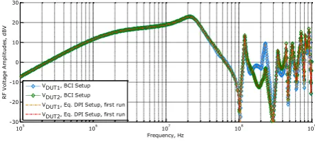
The RF signal levels at both DUTs in the original BCI setup and in equivalent DPI setup are shown in Figs. 10 and 11. In small-signal simulation the RF signals at the first DUT pins are reproduced with high accuracy. The RF source
for-12
105
106
107
108
109
-10 -5 0 5 10 15 20 25 30 35
Frequency, Hz
R
F
Fo
rw
ard
P
o
w
er,
d
B
m
PBCI - Forward power in original BCI Setup PDPI1 - Eq. RF Source 1 incl. test PCB corr. factor PDPI2 - Eq. RF Source 2 incl. test PCB corr. factor PDPI - Total forward power in equivalent DPI
1
Figure 9. RF forward power levels in original BCI and equivalent DPI 2
105
106
107
108
109
-30 -20 -10 0 10 20 30
Frequency, Hz
R
F
V
o
lt
ag
e
A
m
p
lit
u
d
es
,
d
B
V
VDUT1, BCI Setup VDUT2, BCI Setup VDUT1, Eq. DPI Setup, first run VDUT2, Eq. DPI Setup, first run
3
Figure 10. RF levels at first DUT pins under equivalent DPI, first run 4
105
106
107
108
109
-30 -20 -10 0 10 20 30
Frequency, Hz
R
F
V
o
lt
ag
e
A
m
p
lit
u
d
es
,
d
B
V
VDUT3, BCI Setup VDUT4, BCI Setup VDUT3, Eq. DPI Setup, first run VDUT4, Eq. DPI Setup, first run
5
Figure 11. RF signal levels at DUT2 pins under equivalent DPI, first run 6
Fig. 9. RF forward power levels in original BCI and equivalent DPI.
ward power is calculated to reproduce the RF signals at the first DUT. Same RF signal levels are generated at the second DUT too, what obviously doesn not correspond to the orig-inal BCI setup. During the consecutive second run, the eq. forward power is calculated for the second DUT, and both DUTs are tested with this second set of RF signals. Alto-gether, each DUT is at least tested once with a RF disturbance level equivalent to that in original BCI setup. Also none of the DUTs is being overtested, i.e. in no case the RF signals exceed the maximum that might appear at the nodes in orig-inal BCI configuration.
4.4 Advanced testing strategies
The main issue of BCI RF immunity testing in the high fre-quency range is the dependency of the test results on test setup transfer function, which is itself strongly dependent on smaller factors. This leads to instability of correspond-ing BCI RF signal levels and uncertain reproducibility of the test results above 200–300 MHz.
182 S. Miropolsky and S. Frei: Reproducing system-level BCI test in DPI setup 12 105 106 107 108 109 -10 -5 0 5 10 15 20 25 30 35 Frequency, Hz R F Fo rw ard P o w er, d B m
PBCI - Forward power in original BCI Setup PDPI1 - Eq. RF Source 1 incl. test PCB corr. factor PDPI2 - Eq. RF Source 2 incl. test PCB corr. factor PDPI - Total forward power in equivalent DPI
1
Figure 9. RF forward power levels in original BCI and equivalent DPI 2 105 106 107 108 109 -30 -20 -10 0 10 20 30 Frequency, Hz R F V o lt ag e A m p lit u d es , d B V
VDUT1, BCI Setup VDUT2, BCI Setup VDUT1, Eq. DPI Setup, first run VDUT2, Eq. DPI Setup, first run
3
Figure 10. RF levels at first DUT pins under equivalent DPI, first run 4 105 106 107 108 109 -30 -20 -10 0 10 20 30 Frequency, Hz R F V o lt ag e A m p lit u d es , d B V
VDUT3, BCI Setup VDUT4, BCI Setup VDUT3, Eq. DPI Setup, first run VDUT4, Eq. DPI Setup, first run
5
Figure 11. RF signal levels at DUT2 pins under equivalent DPI, first run 6
Fig. 10. RF signal levels at DUT 1 under equiv. DPI, first run.
12 105 106 107 108 109 -10 -5 0 5 10 15 20 25 30 35 Frequency, Hz R F Fo rw ard P o w er, d B m
PBCI - Forward power in original BCI Setup PDPI1 - Eq. RF Source 1 incl. test PCB corr. factor PDPI2 - Eq. RF Source 2 incl. test PCB corr. factor PDPI - Total forward power in equivalent DPI
1
Figure 9. RF forward power levels in original BCI and equivalent DPI 2 105 106 107 108 109 -30 -20 -10 0 10 20 30 Frequency, Hz R F V o lt ag e A m p lit u d es , d B V
VDUT1, BCI Setup VDUT2, BCI Setup VDUT1, Eq. DPI Setup, first run VDUT2, Eq. DPI Setup, first run
3
Figure 10. RF levels at first DUT pins under equivalent DPI, first run 4 105 106 107 108 109 -30 -20 -10 0 10 20 30 Frequency, Hz R F V o lt ag e A m p lit u d es , d B V
VDUT3, BCI Setup VDUT4, BCI Setup VDUT3, Eq. DPI Setup, first run VDUT4, Eq. DPI Setup, first run
5
Figure 11. RF signal levels at DUT2 pins under equivalent DPI, first run 6
Fig. 11. RF signal levels at DUT 2 under equiv. DPI, first run.
PCB layout, termination impedances, and the DUT location. The DUT impedance may be varied in the expected range. By running e.g. Monte-Carlo AC analysis or manually sweeping the parameters the maximum RF levels and corresponding equivalent forward powers can be obtained. By injecting this forward power in an equivalent DPI setup, the maximum pos-sible RF disturbance in BCI can be covered. The success of almost any consequent real BCI test can be assured.
5 Conclusions
A method to reproduce the RF disturbances from a system-level BCI test in a less complex DPI test is proposed. The DPI sources may be attached to the same test PCB as in BCI test. By injecting the equivalent RF forward power (with both amplitude and relative phase being controlled) into the test PCB the same RF disturbance at the DUT can be achieved, and the results of a BCI test can be predicted. The transfer function of the test PCB must be considered in the calculation of the equivalent DPI forward power.
The method is applicable for the systems of multiple DUTs, e.g. for testing communication systems. A test has to be repeated several times, the RF disturbances are sequen-tially reproduced at each DUT in the system, with neither devices being over- nor under-tested after the entire test se-quence is performed.
Acknowledgements. The reported R+D work was partially carried out within the CATRENE project CA310 EM4EM (Electromag-netic Reliability and Electronic Systems for Electro Mobility). This particular research is supported by the BMBF (Bundesministerium fuer Bildung und Forschung) of the Federal Republic of Germany under grant 16 M3092 I. The responsibility for this publication is held by the authors only.
References
Alaeldine, A., Cordi, J., Perdriau, R., Ramdani, M., and Levant, J. L.: Predicting the Immunity of Integrated Circuits through Mea-surement Methods and Simulation Models, 18th Int. Zurich Sym-posium on EMC, Munich 2007.
Crovetti, P. S. and Fiori, F.: Distributed Conversion of Common-Mode Into Differential-Common-Mode Interference, IEEE Tran. on Mi-crowave Theory, Vol. 59, No. 8, August 2011.
Durier, A., Pues, H., Vande Ginste, D., Chernobryvko, M., Gazda, C., and Rogier, H.: Novel Modeling Strategy for a BCI set-up applied in an Automotive Application, EMC Compo 2011, Dubrovnik, Croatia, 2011.
Grassi, F., Marliani, F., and Pignari, S. A.: Circuit Modeling of In-jection Probes for Bulk Current InIn-jection, IEEE Tran., EMC 49, No. 3, 563–576, 2007.
Gustavsen, B. and Semlyen, A.: Rational Approximation of Fre-quency Domain Responses by Vector Fitting, IEEE Tran. on Power Delivery, 14, 1052–1061, 1999.
IEC 62132-4: Integrated Circuits – Measurement of Electromag-netic Immunity 150 kHz to 1 GHz – Part 4: Direct RF Power Injection Method, 2006.
ISO 11452-4: Road Vehicles – Component Test Methods for Elec-trical Disturbances from Narrowband Radiated Electromagnetic Energy – Part 4: Bulk Current Injection (BCI), ISO, 2005. Lafon, F., Belakhouy, Y., and De Daran, F.: Injection Probe
Mod-eling for Bulk Current Injection Test on Multiconductor Trans-mission Lines, IEEE Symp. on Embedded EMC Proceedings, Rouen, France, 2007.
Miropolsky, S. and Frei, S.: Comparability of RF Immunity Test Methods for IC Design Purposes, EMC Compo 2011, Dubrovnik, Croatia, 2011.
Miropolsky, S., Frei, S., and Frensch, J.: Modeling of Bulk Current Injection Setups for Virtual Automotive IC Tests, EMC Europe 2011, Wroclaw, Poland, 2011.
Oguri, Y. and Ichikawa, K.: Simulation Method for Automotive Electronic Equipment Immunity Testing, EMC Europe 2012, Rome, Italy, 2012.