Management and Research
Available online at: www.ijstmr.comIJSTMR
©
2016 | All Rights Reserved90
Implementation of Digital Current Sensorless
Control for Dual-Boost Half bridge PFC
Converter with Natural Capacitor Voltage
Balancing
Charushila Gangurde E & TC Department GES RHSCOE, MS&R
Nashik, India.
Prof.Agnihotri S.P. Head E & TC Department
GES RHSCOE, MS&R Nashik, India. Prof.S.K.Pund Electrical Department SIER, Agaskhind Nashik, India _________________________________________________________________________________________________
Abstract-:The Power Factor Correction (PFC) converters of bridgeless category are often used to improve the efficiency of the
conventional boost-type power factor correction (PFC) converters with the diode bridge circuit. The short circuit problems are not
occurred due to non inability of series connected switches for improving PFC Dual boost Half-bridge circuit is used. The DBHB PFC
converter model is developed in added to simplified the conventional two loop Control scheme and reduce the number of current
sensors. Then, the current sensor-less control for DBHB PFC converter is proposed to achieve voltage regulation and yield sinusoidal
input current in phase with the input voltage without sensing any current. In addition, the proposed method is able to balance
capacitor voltages naturally without adding any voltage balancing control loop. The above maintain method we proposed for
observing the performance of the DBHB PFC planning to design in Matlab / Simulation and planning for experimental setup.
Keywards:Power factor,Pfc,Converter,IGBT, Current sensorless control(CSC).
________________________________________________________________________________________________________
I. INTRODUCTION
1.1 Power Factor:-
Power factor is defined as the cosine of the angle between voltage and current in an ac circuit. There is generally a phase difference Ø between voltage and current in an ac circuit. cos Ø is called the power factor of the circuit. If the circuit is inductive, the current lags behind the voltage and power factor is referred to as lagging. However, in a capacitive circuit, current leads the voltage and the power factor is said to be leading.
In a circuit, for an input voltage V and a line current I, 1) VIcos Ø –the active or real power in watts or kW. 2) VIsin Ø- the reactive power in VAR or kVAR. 3) VI- the apparent power in VA or kVA.
Power Factor gives a measure of how effective the real power utilization of the system is. It is a measure of distortion of the line voltage and the line current and the phase shift between them. Power Factor=Real power (Average)/Apparent power
IJSTMR
©
2016 | All Rights Reserved91
1.2 Power Electronic Systems:-In power electronic system, due to the non-linear behavior of the active switching power devices, the phase angle representation alone is not valid. A non linear load draws typical distorted line current from the line. The PF of distorted waveforms is calculated as below:
The Fourier representation for line current is and line voltage vs are given by, is = IDC + ΣIsnsin(nωt+θ)
vs=VDC +ΣVsnsin(nωt+θ)
The line current is non-sinusoidal when the load is nonlinear. For sinusoidal voltage and non- sinusoidal current the PF can be expressed as
Where, cosΦ is the displacement factor of the voltage and current. Kp is the purity factor or the distortion factor.
Another important parameter that measures the percentage of distortion is known as the current total harmonic distortion (THDi) which is defined as follows:
Hence the relation between Kp and THDi is
1.3 Power Factor Correction:-
Power factor correction is the term given to a technology that has been used since the turn of the 20th century to restore the power factor to as close to unity as is economically viable. This is normally achieved by the addition of capacitors to the electrical network which compensate for the reactive power demand of the inductive load and thus reduce the burden on the supply. There should be no effect on the operation of the equipment.
1.3.1 Types of Power Factor Correction:-
A) Passive Power Factor Correction (PFC):-
Harmonic current can be controlled in the simplest way by using a filter that passes current only at line frequency (50 or 60 Hz).Harmonic currents are suppressed and the non-linear device looks like a linear load. Power factor can be improved by using capacitors and inductors i.e. passive devices. Such filters with passive devices are called passive filters.
Disadvantage:-They require large value high current inductors which are expensive and bulky. A passive PFC circuit requires only a few components to increase efficiency, but they are largedue to operating at the line power frequency
B) Active Power Factor Correction (PFC) :-
An active approach is the most effective way to correct power factor of electronic supplies. Here, we place a boost converter between the bridge rectifier and the main input capacitors. The converter tries to maintain a constant DC output bus voltage and draws a current that is in phase with and at the same frequency as the line voltage.
IJSTMR
©
2016 | All Rights Reserved92
There are numerous benefits to be gained through power factor correction. These benefits range from reduced demand charges on your power system to increased load carrying capabilities in your existing circuits and overall reduced power system loses. And the benefits of power factor correction aren’t just limited to the balance sheet; there are also huge environmental benefits associated with power factor correction, which means your company is reducing its carbon footprint and helping the environment.1) Reduced Demand Charges:-
Most electric utility companies charge for maximum metered demand based on either the highest registered demand in kilowatts (KW meter), or a percentage of the highest registered demand in KVA (KVA meter), whichever is greater. If the power factor is low, the percentage of the measured KVA will be significantly greater than the KW demand. Improving the power factor through power factor correction will therefore lower the demand charge, helping to reduce your electricity bill.
2) Increased Load Carrying Capabilities In Existing Circuits:-
Loads drawing reactive power also demand reactive current. Installing power factor correction capacitors at the end of existing circuits near the inductive loads reduces the current carried by each circuit. The reduction in current flow resulting from improved power factor may allow the circuit to carry new loads, saving the cost of upgrading the distribution network when extra capacity is required for additional machinery or equipment, saving your company thousands of dollars in unnecessary upgrade costs. In addition, the reduced current flow reduces resistive losses in the circuit.
3) Improved Voltage:-
A lower power factor causes a higher current flow for a given load. As the line current increases, the voltage drop in the conductor increases, which may result in a lower voltage at the equipment. With an improved power factor, the voltage drop in the conductor is reduced, improving the voltage at the equipment
4. Reduced Power System Losses:-
Although the financial return from conductor loss reduction alone is seldom sufficient to justify the installation of capacitors, it is sometimes an attractive additional benefit; especially in older plants with long feeders or in field pumping operations. System conductor losses are proportional to the current squared and, since the current is reduced in direct proportion to the power factor improvement, the losses are inversely proportional to the square of the power factor.
5. Reduced Carbon Footprint:-
By reducing your power system’s demand charge through power factor correction, your company is putting less strain on the electricity grid, therefore reducing its carbon footprint. Over time, this lowered demand on the electricity grid can account for hundreds of tons of reduced carbon production, all thanks to the improvement of your power system’s electrical efficiency via power factor correction
II. Fundamentals of Power Electronics
Power electronics (PE) experienced tremendous growth after the introduction of the first solid-state power switch, the silicon controlled rectifier (SCR) in 1957. Today, almost all of the technologies that require control of power control utilize PE technology. The modern PE era began in 1957. It was during that year the first commercial thyristor, or Silicon Controlled Rectifier (SCR), was introduced by General Electric Company. The SCR, started replacing the mercury arc rectifiers, invented in 1902, and the later developed thyratron (invented in 1923) and ignitron (invented in 1931), allowed the commercialization of several industrial circuits conceived during the 1920s and 1940s (like the cyclo converter, the chopper, and the parallel inverter) as well as the Graetz bridge conceived in 1897.
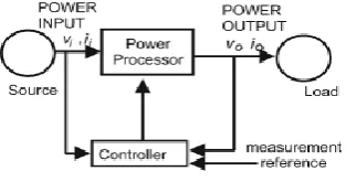
Fig 1:- A general power electronic system.
IJSTMR
©
2016 | All Rights Reserved93
capabilities, with better controllability were developed, including the bipolar junction transistor (BJT) invented in 1970. The BJT was used in applications from low to medium power and frequency and now is considered obsolete. The metal oxide semiconductor field effect transistor (MOSFET) was invented in 1978 and is used for power electronic switching applications of low power and high frequencies. The gate turn-off thermistor (GTO), is used in applications from medium to high power and from low to medium frequencies. The insulated gate bipolar transistor (IGBT) developed in 1983 is used in applications from low to medium power and frequency. The integrated gate commutated thermistor (IGCT) invented in 1997 is used in applications from medium to high power and from low to medium frequencies.III. BOOST CONVERTERS & INSULATED GATE BIPOLAR TRANSISTOR (IGBT) 3.1 Principle of Step-Up Operation (Boost Converter):-
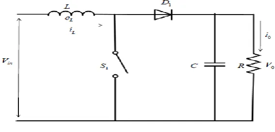
The circuit diagram of a step up operation of Boost Converter is shown in Figure . The output voltage is always greater than the input voltage. When the switch is closed for time duration, the inductor current rises and the energy is stored in the inductor. If the switch is openerd for time duration, the energy stored in the inductor is transferred to the load via the diode and the inductor current falls. The waveform of the inductor current is shown in Figure.
Fig 2:-General Configuration of a Boost Converter
.
Figure 3:-Inductor current waveform
When the switch is turned on, the voltage across the inductor is
The peak to peak ripple current in the inductor is given by
IJSTMR
©
2016 | All Rights Reserved94
From Equation 3 the following observations can be made:- The voltage across the load can be stepped up by varying the duty ratio D ;The minimum output voltage is Vs and is obtained when D=0 ;The converter cannot be switched on continuously such that D=1. For values of D tending to unity, the output becomes very sensitive to changes in D .For values of D tending to unity, the output becomes very sensitive to changes inFig.4:-Output voltage vs. Duty ration for Boost Converter
IV.PROPOSED CURRENT SENSORLESS CONTROL
4.1 Current Sensor less
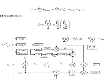
Control:-In order to reduce the current sensor, the single-loop current sensorless control is proposed. The proposed current sensorless control is able to regulate the output voltage Vo and shape the input current is in phase with the input voltage vs . For the PFC function, the desired average current can be expressed as the sin(t) function
Therefore, the average inductor voltage <vL>Ts should be forced to the cos(t) expression
where the value VˆL =LIˆs can be seen as the amplitude of the inductor voltage<vL>Ts
IJSTMR
©
2016 | All Rights Reserved95
The average power P can be expressed asFig. 5: Proposed current sensor less control scheme
It shows that the average power is proportional to the controller output VˆL . From Fig. 4.1, the integrator tunes the voltage amplitude signal VˆL . It follows that a simple integrator controller is able to balance the average power flow and thus, regulate the output voltage.
Conclusion
The single-switch model for Dual-Boost Half Bridge (DBHB) PFC converter has been developed. The current sensor-less control method for DBHB PFC converter has been proposed and implemented in this paper. The Power Factor Correction (PFC) converters of bridgeless category are often used to improve the efficiency of the conventional boost-type power factor correction (PFC) converters with the diode bridge circuit. The short circuit problems are not occurred due to non inability of series connected switches for improving PFC Dual boost Half-bridge circuit is used. The DBHB PFC converter model is developed in added to simplified the conventional two loop control scheme and reduces the number of current sensors. The integrator-type voltage controller is able to regulate the output voltage and balance the capacitor voltages. The proposed control strategy effectively achieves PFC function in steady-state condition and transient condition. Moreover, the capacitor voltages can be naturally balanced by the proposed control method. This control method can be used to the half-bridge PFC converter due to the same single-switch model.
REFERENCES
1. R. Srinivasan and R. Oruganti, “A Unity Power Factor Converter Using Half-Bridge Boost Topology,” IEEE Trans. Power Electron, vol. 13, May 1998.
2. Liu and K. Smedley, “Control of a Dual Boost Power Factor Corrector for High Power Applications,” in Proc. IEEE IECON, 2003.
M. H. Rashid, Power Electronics: Circuits, Devices and Applications, 3rd edition, Pearson, 2004
3. M. Chen and J. Sun, “Feed-forward Current Control of Boost Single-Phase PFC Converters,” IEEE Trans. Power Electron, vol. 21, Feb. 2006.
4. R. Ghosh and G. Narayanan, “A Simple Analog Controller for Single-Phase Half-Bridge Rectifier,” IEEE Trans. Power Electron, vol. 22, Jan. 2007.
5. H. C. Chen, H. Y. Li and R. S. Yang, “Phase Feed-forward Control for Single-Phase Boost-Type SMR,” IEEE Trans. Power Electron. vol. 24, May 2009.
IJSTMR
©
2016 | All Rights Reserved96
7. F. J. Azcondo, and A. de Castro, V. M. Lopez, and O. Garcia, “Power Factor Correction without Current Sensor Based on Digital Current Rebuilding,” IEEE Trans. on Power Electronics, vol. 25, Jan. 2010.
8. J. M. Wang, S. T. Wu, Y. Jiang, and H. J. Chiu, “A Dual-Mode for the Boost PFC Converter,” IEEE Trans. Ind. Electron., vol. 58, Jan. 2011.
9. S. M. Park, Y. D. Lee, and S. Y. Park, “Voltage Sensor-less Feed-forward Control of a Dual Boost PFC Converter for Battery Charger Applications,” in Proc. Energy Convers. Cong. Expo. (ECCE), 2011.
10. H. C. Chen, C. C. Lin, and J. Y. Liao, “Modified Single-Loop Current Sensor-less Control for Single-Phase Boost-Type SMR With Distorted Input Voltage,” IEEE Trans. Power Electron., vol. 26, May 2011.
11. P. Fang and Y. F. Liu, “A Innovative Current Sensor-less Continuous Conduction Mode PFC Control,” in Proc. IEEE ECCE Conf., 2013.
12. Che-Yu Lu, Hung-Chi Chen, Wei-Cheng Chen and Chung-Yi Li “Current Sensor-less Control for Dual-Boost Half-Bridge PFC Converter” IEEE Conf, 2015.
13. Power Electronics, National Programme on Technology Enhanced Learning; Lesson 7 (Insulated Gate Bipolar Transistor) Version 2 EE IIT, Kharagpur, 2016.