Available Online at www.ijpret.com 994
INTERNATIONAL JOURNAL OF PURE AND
APPLIED RESEARCH IN ENGINEERING AND
TECHNOLOGY
A PATH FOR HORIZING YOUR INNOVATIVE WORKFIELD PROGRAMMABLE GATE ARRAY
MS. HITAISHEE V. DESHMUKH
Department of Electronics and Telecommunication, H.V.P.M’s. C.O.E.&T., SGBAU Amravati
Accepted Date: 05/03/2015; Published Date: 01/05/2015
\
Abstract: This report concerns with FPGAs (Field Programmable Gate Arrays). Field Programmable
Gate Arrays (FPGAs) were first introduced almost two and a half decades ago. Since then they have seen a rapid growth and have become a popular implementation media for digital circuits. The advancement in process technology has greatly enhanced the logic capacity of FPGAs and has in turn made them a viable implementation alternative for larger and complex designs. Further, programmable nature of their logic and routing resources has a dramatic effect on the quality of final device’s area, speed, and power consumption. This report covers different aspects related to FPGAs. First of all an overview of the basic FPGA architecture is presented. An FPGA comprises of an array of programmable logic blocks that are connected to each other through programmable interconnect network. Programmability in FPGAs is achieved through an underlying programming technology. This report briefly discusses the details of basic FPGA logic blocks and different routing architectures. After that, an overview of the different steps involved in FPGA design flow is given. This report discusses the basic architecture and functioning of FPGAs along with its strengths and weaknesses.
Keywords: FPGA, logic blocks, LUT, programmable
Corresponding Author: MS. HITAISHEE V. DESHMUKH
Access Online On:
www.ijpret.com
How to Cite This Article:
Available Online at www.ijpret.com 995
INTRODUCTION
Field-programmable gate arrays (FPGAs) arrived in 1984 as an alternative to programmable logic devices (PLDs) and ASICs. As the name implies, FPGAs offer the significant benefit of being readily programmable. Unlike their forbearers in the PLD category, FPGAs can (in most cases) be programmed again and again, giving designers multiple opportunities to tweak their circuits. There’s no large non-recurring engineering (NRE) cost associated with FPGAs. In addition, lengthy, nerve-wracking waits for mask-making operations are squashed. Often, with FPGA development, logic design begins to resemble software design due to the many iterations of a given design. Innovative design often happens with FPGAs as an implementation platform. But there are some downsides to FPGAs as well. The economics of FPGAs force designers to balance their relatively high piece-part pricing compared to ASICs with the absence of high NREs and long development cycles. They’re also available only in fixed sizes, which matters when you’re determined to avoid unused silicon area.
FPGAs fill a gap between discrete logic and the smaller PLDs on the low end of the complexity scale and costly custom ASICs on the high end. They consist of an array of logic blocks that are configured using software. Programmable I/O blocks surround these logic blocks. Both are connected by programmable interconnects. The programming technology in an FPGA determines the type of basic logic cell and the interconnect scheme. In turn, the logic cells and interconnection scheme determine the design of the input and output circuits as well as the programming scheme. . Also found on today’s FPGAs are system-building resources such as high speed serial I/Os, arithmetic modules, embedded processors, and large amounts of memory. Initially seen as a vehicle for rapid prototyping and emulation systems, FPGAs have spread into a host of applications. They were once too simple, and too costly, for anything but small-volume production. Now, with the advent of much larger devices and declining per-part costs, FPGAs are finding their way off the prototyping bench and into production.[1]
FPGA families can be used to meet a range of processing, display, and I/O interface requirements. Xilinx offers solutions that meet the evolving needs of security applications, from access control to surveillance and safety systems.[2]
Literature Review
Available Online at www.ijpret.com 996 control operations, and almost every other function a system must perform. The first type of user-programmable chip that could implement logic circuits was the Programmable Read-Only Memory (PROM), in which address lines can be used as logic circuit inputs and data lines as outputs. Logic functions, however, rarely require more than a few product terms, and a PROM contains a full decoder for its address inputs. PROMS are thus an inefficient architecture for realizing logic circuits, and so are rarely used in practice for that purpose. The device that came as a replacement for the PROM’s are programmable logic devices or in short PLA. Logically, a PLA is a circuit that allows implementing Boolean functions in sum-of-product form. The typical implementation consists of input buffers for all inputs, the programmable AND-matrix followed by the programmable OR-matrix, and output buffers. The input buffers provide both the original and the inverted values of each PLA input. The input lines run horizontally into the AND matrix, while the so-called product-term lines run vertically. Therefore, the size of the AND matrix is twice the number of inputs times the number of product-terms. [1]
When PLAs were introduced in the early 1970s, by Philips, their main drawbacks were that they were expensive to manufacture and offered somewhat poor speed-performance. Both disadvantages were due to the two levels of configurable logic, because programmable logic planes were difficult to manufacture and introduced significant propagation delays. To overcome these weaknesses, Programmable Array Logic (PAL) devices were developed. PALs provide only a single level of programmability, consisting of a programmable “wired” AND plane that feeds fixed OR-gates. PALs usually contain flip-flops connected to the OR-gate outputs so that sequential circuits can be realized. These are often referred to as Simple Programmable Logic Devices (SPLDs). Fig.1 shows the simplified structure of PAL. [3]
Available Online at www.ijpret.com 997 With the advancement of technology, it has become possible to produce devices with higher capacities than SPLD’s. As chip densities increased, it was natural for the PLD manufacturers to evolve their products into larger (logically, but not necessarily physically) parts called Complex Programmable Logic Devices (CPLDs). For most practical purposes, CPLDs can be thought of as multiple PLDs (plus some programmable interconnect) in a single chip. The larger size of a CPLD allows to implement either more logic equations or a more complicated design. Unlike the programmable interconnect within a PLD, the switch matrix within a CPLD may or may not be fully connected. In other words, some of the theoretically possible connections between logic block outputs and inputs may not actually be supported within a given CPLD. The effect of this is most often to make 100% utilization of the macro cells very difficult to achieve. Some hardware designs simply won't fit within a given CPLD, even though there are sufficient logic gates and flip-flops available. Because CPLDs can hold larger designs than PLDs, their potential uses are more varied. They are still sometimes used for simple applications like address decoding, but more often contain high-performance control-logic or complex finite state machines. At the high-end (in terms of numbers of gates), there is also a lot of overlap in potential applications with FPGAs. Traditionally, CPLDs have been chosen over FPGAs whenever high-performance logic is required. Because of its less flexible internal architecture, the delay through a CPLD (measured in nanoseconds) is more predictable and usually shorter.
FPGAs offer the highest amount of logic density, the most features, and the highest performance. FPGAs are used in a wide variety of applications ranging from data processing and storage, to instrumentation, telecommunications, and digital signal processing. The value of programmable logic has always been its ability to shorten development cycles for electronic equipment manufacturers and help them get their product to market faster. As PLD (Programmable Logic Device) suppliers continue to integrate more functions inside their devices, reduce costs, and increase the availability of time-saving IP cores, programmable logic is certain to expand its popularity with digital designers. [2]
III ARCHITECTURE OF FPGA
Available Online at www.ijpret.com 998 technology, which is a method that can cause a change in the behavior of the pre-fabricated chip after fabrication, in the “field,” where system users create designs.
The fig.2 shows the general structure of FPGA chip. It consists of a large number of programmable logic blocks surrounded by programmable I/O block. The programmable logic blocks of FPGA are smaller and less capable than a PLD, but an FPGA chip contains a lot more logic blocks to make it more capable. As shown in fig.2 the logic blocks are distributed across the entire chip. These logic blocks can be interconnected with programmable inter connections.
The programmable logic blocks in the Xilinx family of FPGAs are called Configurable Logic Blocks (CLBs).The architecture uses, CLBs, I/O blocks switch matrix and an external memory chip to realize a logic function. It uses external memory to store the interconnection information. Therefore, the device can be reprogrammed by simply changing the configuration data stored in the memory.
The basic structure of an FPGA is composed of the following elements:
CLBs: Configurable Logic Blocks
Programmable Interconnects
Input/Output (I/O) ports: These physically available ports get data in and out of the
Look-up table (LUT): This element performs logic operations.
Flip-Flop (FF): This register element stores the result of the LUT.
Available Online at www.ijpret.com 999 Configurable Logic Block:
The CLB contains RAM memory cells and can be programmed to realize any function of five variables or any two functions of four variables. The functions are stored in the truth table form, so the number of gates required to realize the functions is not important. In the above fig each trapezoidal block represents a multiplexer, which can be programmed to select one of its inputs.
Fig.3 Combinational logic array, program controlled data multiplexers, and flip-flops.
Programmable Interconnect:
The programmable interconnections between the configurable logic blocks and I/O blocks can be made in several ways
(1)General purpose interconnects
(2)Direct interconnect
(3)Vertical & Horizontal Long Line interconnect e
Available Online at www.ijpret.com 1000 2) Direct Interconnect: Direct interconnection of adjacent CLBs is possible. Long lines are provided to connect CLBs that are far apart. All the interconnections are programmed by storing bits in internal configuration memory cells within the LCA. Long lines provide for high fan-out, low-skew distribution of signals that must travel a relatively long distance.
3) Vertical & Horizontal Long Line interconnects: There are four vertical long lines between each pair of adjacent columns of CLBs, and two of these can be used for clocks. There are two horizontal long lines between each pair of adjacent rows of CLBs. The long line spans the entire length or width of the interconnection area.[10]
Look Up Table:
The LUT is the basic building block of an FPGA and is capable of implementing any logic function of N Boolean variables. Essentially, this element is a truth table in whichdifferent combinations of the inputs implement different functions to yield output values. The limit on the size of the truth table is N, where N represents the number of inputs to the LUT. For the general N-input LUT, the number of memory locations accessed by the table is:
2N
The hardware implementation of a LUT can be thought of as a collection of memory cells connected to a set of multiplexers. The inputs to the LUT act as selector bits on the multiplexer to select the result at a given point in time. It is important to keep this representation in mind, because a LUT can be used as both a function compute engine and a data storage element.
Flip Flops:
The flip-flop is the basic storage unit within the FPGA fabric. This element is always paired with a LUT to assist in logic pipelining and data storage. The basic structure of a flip-flop includes a data input, clock input, clock enable, reset, and data output. During normal operation, any value at the data input port is latched and passed to the output on every pulse of the clock. The purpose of the clock enable pin is to allow the flip-flop to hold a specific value for more than one clock pulse. New data inputs are only latched and passed to the data output port when both clock and clock enable are equal to one.[4]
Programming Technologies
Available Online at www.ijpret.com 1001 emerged to suit different requirements. Some FPGAs can only be programmed once. These devices employ antifuse technology. Flash-based devices can be programmed and reprogrammed again after debugging. Still others can be dynamically programmed thanks to SRAM-based technology. Each has its advantages and disadvantages[1]
1) Static RAM Programming Technology:
Static memory cells are the basis for SRAM programming technology which is widely used and can be found in devices from Xilinx ([29],[35]), Lattice ([13], [14]), and Altera ([5], [6],[7]). In these devices, static memory cells, such as the
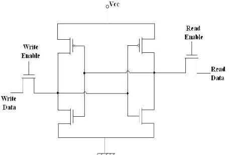
one shown in Figure.4, are distributed throughout the FPGA to provide configurability. There are two primary uses for the SRAM cells. Most are used to set the select lines to multiplexers that steer interconnect signals. The majority of the remaining SRAM cells are used to store the data in the lookup-tables (LUTs) that are typically used in SRAM-based FPGAs to implement logic functions. SRAM programming technology has become the dominant approach for FPGAs because of its two primary advantages: re-programmability and the use of standard CMOS process technology. From a practical standpoint, an SRAM cell can be programmed an indefinite number of times. Dedicated circuitry on the FPGA initializes all the SRAM bits on power up and configures the bits with a user-supplied configuration. Unlike other programming technologies, the use of SRAM cells requires no special integrated circuit processing steps beyond standard CMOS. As a result, SRAM-based FPGAs can use the latest CMOS technology available and, therefore, benefit from the increased integration, the higher speeds and the lower dynamic power consumption of new processes with smaller minimum geometries.
Available Online at www.ijpret.com 1002 2) Flash/EEPROM Programming Technology:
One alternative that addresses some of the shortcomings of SRAM based technology is the use of floating gate programming technologies that inject charge onto a gate that “floats” above the transistor. This approach is used in flash or EEPROM memory cells. With modern IC fabrication processes, it has become possible to use the floating gate cells directly as switches. Flash memory cells, in particular, are now used because of their improved area efficiency. The widespread use of flash memory cells for non-volatile memory chips ensures that flash manufacturing processes will benefit from steady decreases in process geometries. Figure 5 illustrates the flash-based approach used in Actel’s ProASIC devices *2, 19].
Fig. 5 Float Gate Transistor
Available Online at www.ijpret.com 1003 many cases FPGAs are programmed for only one use. Another significant disadvantage of flash devices is the need for a non-standard CMOS process. Also, like the static memory-based technology, this programming technology suffers from relatively high resistance and capacitance due to the use of transistor-based switches. One trend that has recently emerged is the use of flash storage in combination with SRAM programming technology ([6],[2]). It is important to recognize that, since the programming technology is still based on SRAM cells, the devices are no different than pure-SRAM based devices from an FPGA architecture standpoint. However, the incorporation of flash memory generally means that the processing technology will not be as advanced as pure-SRAM devices. Additionally, the devices incur more area overhead than pure-SRAM devices since both flash and SRAM bits are required for every programmable element.[11]
3) Anti-fuse Programming Technology:
Non-Available Online at www.ijpret.com 1004 volatility also means that the device works instantly once programmed. This lowers system costs since additional memory for storing the programming information is not required and it also allows the FPGA to be used in situations that require operation immediately upon power up. There are also significant disadvantages to this programming technology. In particular, since anti-fuse-based FPGAs require a nonstandard CMOS process, they are typically well behind in the manufacturing processes that they can adopt compared to SRAM-based FPGAs. Furthermore, the fundamental mechanism of programming, which involves significant changes to the properties of the materials in the fuse, leads to scaling challenges when new IC fabrication processes are considered.
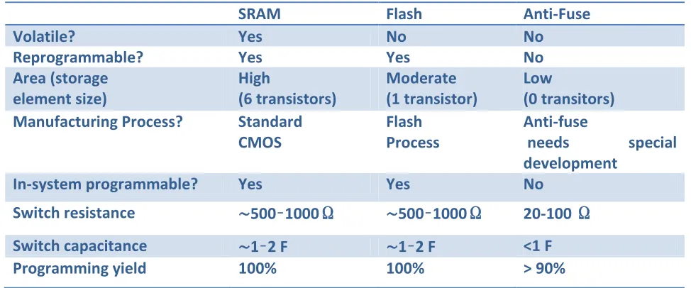
Table 1 Programming technology properties summary.
SRAM Flash Anti-Fuse
Volatile? Yes No No
Reprogrammable? Yes Yes No
Area (storage element size) High (6 transistors) Moderate (1 transistor) Low (0 transitors)
Manufacturing Process? Standard
CMOS
Flash Process
Anti-fuse
needs special
development
In-system programmable? Yes Yes No
Switch resistance ∼500–1000Ω ∼500–1000Ω 20-100 Ω
Switch capacitance ∼1–2 F ∼1–2 F <1 F
Programming yield 100% 100% > 90%
Applications
Available Online at www.ijpret.com 1005 necessary software to partition and map circuits. Another promising area for FPGA application, which is only beginning to be developed, is the usage of FPGAs as custom computing machines. This involves using the programmable parts to “execute” software, rather than compiling the software for execution on a regular CPU. [14]
1) Radar and Sonar: Radar systems – for air, ground, and sea — must keep size, weight, and power to a minimum while still being able to execute sophisticated processing algorithms in real time. Sonar systems – for detecting objects in water such as subs, torpedoes, and ocean topography – must be adaptable to a broad array of computational requirements. Both need flexible solutions that are capable of conforming to their many data processing requirements. Many high-speed signal processing solutions featuring both FPGAs and processors, allowing system designers to adapt the system to their exact needs can be offered.
2)Weapons : Many new weapon designs feature embedded high-performance computing. To meet the demands of these designs, BittWare offers COTS solutions that are ruggedized and conduction cooled, featuring both FPGAs and DSPs. The combination of FPGAs and DSPs provides extra processing power and allows designers flexibility in developing their applications.
2)Unmanned Vehicles: Unmanned vehicles must process a barrage of signals to assess multiple potential threats. They must keep power, size, and weight to a minimum; and they require processing architectures that are reconfigurable and can perform real-time processing. COTS solutions that combine FPGAs to allow for scalable, reconfigurable designs in high-speed signal processing are available.
3)Software Defined Radio: Software defined radio solutions must be compatible with the many different types of waveforms, and they must be able to detect and remove interference. To do so, they need to be reconfigurableand adaptable. BittWare offers many FPGA board solutions, which provide reconfigurability and allow the designer flexibility in developing their systems.
4) Wireless Infrastructure: Wireless infrastructure applications must keep up with the latest wireless protocol as well as processing a barrage of signals. To address these needs, a product line has been developed that melds FPGA technology, creating a reconfigurable.
Available Online at www.ijpret.com 1006 provide a high level of flexibility and reprogrammability, so that the system is, to some extent, a general-purpose one that can be tailored to the needs of individual applications. To meet the needs of inspection and control systems designers, a line of hybrid signal processing boards designed that combine FPGAs and DSPs with an innovative architecture.
6) Cytometry: High-end bioscience applications often require automated inspection and control to perform tasks that would otherwise be impossible, since they cannot be done manually. The sorting and classification of biological cells via flow cytometry and cell sorting is one such area. These flow cytometry and cell sorting systems have traditionally used complex, custom analog circuitry that has remained unchanged for many years. However, work has been done with customers to develop systems that use of FPGAs working to provide the processing. The result is intelligent systems that also provide a high level of flexibility and reprogrammability, enabling them to be somewhat general purpose, yet capable of being tailored to the requirements of specific applications.
Closing Comments
The flexibility of FPGAs gives them a distinct advantage over other programmable logic devices on the market. The advantage is most apparent in application where time to market concerns are paramount3. Because FPGAs are reprogrammable and can implement any sort of logic circuit, designs can be modified after initial implementation. With one time programmable technologies such as AISCs, logic is set at the factory and no changes can be made after manufacture. The drawbacks to FPGA use involve speed and space. Switching gate resistances and capacitances make for slow logic and poor logic density.
REFERENCES
1. Actel Corporation, “ProASIC3 flash family FPGAs,”
http://www.actel.com/documents/PA3 DS.pdf , October 2005.
2. Xilinx,“Spartan-3AN FPGA family data sheet, DS557,”
http://www.direct.xilinx.com/bvdocs/publications/ds557.pdf , February 2007.
3. Actel Corporation, “Axcelerator family FPGAs,” http://www.actel.com/documents/AX DS.pdf
, May 2005.
Available Online at www.ijpret.com 1007 5. Altera Corporation, “Stratix II device handbook SII5V13.1,”
http://www.altera.com/literature/hb/stx2/stratix2 handbook.pdf , July 2005.
6. Altera Corporation, “Cyclone II device handbook, ver. CII5V1-3.0,”
http://www.altera.com/literature/hb/cyc2/cyc2 cii5v1.pdf , June 2006.
7. Altera Corporation, “Cyclone III device handbook, ver. CIII5V1-1.2,”
http://www.altera.com/literature/hb/cyc3/cyclone3 handbook.pdf , September 2007.
8. J. Chen, S. Eltoukhy, S. Yen, R. Wang, F. Issaq, G. Bakker, J. L. Yeh, E. Poon, D. Liu, and E. Hamdy, “A modular 0.8 um technology for high performance dielectric antifuse field programmable gate arrays,” in Proceedings of 1993 International Symposium on VLSI Technology, Systems and Applications, pp. 160–164, 1993.
9. K. E. Gordon and R. J. Wong, “Conducting filament of the programmed metal electrode amorphous silicon antifuse,” in International Electron Devices Meeting, 1993. Technical Digest., International, pp. 27–30, 1993.
10. J. Greene, E. Hamdy, and S. Beal, “Antifuse field programmable gate arrays,” Proceedings of the IEEE, vol. 81, no. 7, pp. 1042–1056, July 1993.
11. E. Hamdy, J. McCollum, S.-O. Chen, S. Chiang, S. Eltoukhy, J. Chang, T. Speers, and A. Mohsen, “Dielectric based antifuse for logic and memory IC,” in International Electron Devices Meeting Technical Digest, pp. 786–789,December
12. S. Chiang, R. Forouhi, W. Chen, F. Hawley, D. McCollum, E. Hamdy, and C. Hu, “Antifuse structure comparison for field programmable gate arrays,” in International Electron Devices Meeting 1992 Technical Digest, pp. 611–614, December 1992.
13. Lattice Semiconductor Corporation, “LatticeECP/EC family data sheet, version02.0,”
http://www.latticesemi.com/lit/docs/datasheets/fpga/ecpecdatasheet.pdf, September 2005.
14. Lattice Semiconductor Corporation, “LatticeSC family data sheet DS1004 version 01.5,”
http://www.latticesemi.com/dynamic/view document.cfm?document id=19028 , March
15. R. Lipp, R. Freeman, and T. Saxe, “A high density flash memory FPGA family,” in Proceedings of the IEEE Custom Integrated Circuits Conference, pp. 239–242, May 1996.
Available Online at www.ijpret.com 1008 17. QuickLogic Corporation, “Eclipse II family data sheet (Rev P),”
http://www.quicklogic.com/images/EclipseII Family DS.pdf , February 2007.
18. QuickLogic Corporation, “QuickLogic PolarPro Data Sheet (Rev H),”
http://www.quicklogic.com/images/polarpro DS.pdf , February 2007.
19. T. Speers, J. J. Wang, B. Cronquist, J. McCollum, H. Tseng, R. Katz, and I. Kleyner, “0.25 um flash memory based FPGA for space applications,” in MAPLD Conference, Baltimore MD, 1999. www.actel.com/documents/ FlashSpaceApps.
20. Xilinx, “Spartan-II 2.5V FPGA family complete data sheet,”
http://www.eecg.toronto.edu/~jayar/pubs/kuon/foundtrend08.pdf ,
21. Xilinx, “Virtex-5 user guide,” UG190 (v2.1), October 2006.