International Journal of Research
Available at https://edupediapublications.org/journalse-ISSN: 2348-6848 p-ISSN: 2348-795X Volume 05 Issue 19
August 2018
Study Of Electrical and Optical Properties Of Thin Films
Hayder Hasan Ali Alhasnawi 1 , Hayder Hasan Ali Alowaid 2
1,2Bachelor of Science(Physics)
University of Sumer College of basic Education, Thi Qar, Iraq
1,2
Abstract
The planning and properties of
phosphorus-doped SnO2 films, deposited on a warmed
borosilicate glass utilizing the concoction vapor testimony, are accounted for in this paper. It is watched that the resistivity of the film reductions and its carrier focus increments as the doping grouping of phosphorus increments up to 3.7 wt.%.
Sputtering powers of 0.375– 0.750
W/cm2 and of 0.750 W/cm2 were
connected, individually, to
the tin and tungsten targets so as to
obtain films with diverse Sn/W proportions. The deposited amorphous films were anneal ed for four hours at 400 °C keeping in mind the end goal to solidify the films.
The films sputtered with 0.750 W/cm2 power
for the two modes were found to have
α‐SnWO4 structure crystalline after
annealing. Electrical resistivity of the films
was measured at different temperatures
between room temperature and 400 °C in engineered air and in nitrogen. The
resistivity changes of the films at
presentation to carbon monoxide were
also measured at different temperatures
between room temperature and 400 °C.
Optical reflectance and transmittance
spectra of the films were recorded in the
0.3<λ<2.5 μm range, and the genuine and nonexistent parts of the mind boggling refraction file were registered in the visible range.
Keywords:- Reflectance spectra, structure
crystalline,thin film, transmission
contrasted,Optical properties
INTRODUCTION:
The SnO2 thin film has a transparent
electrode and has a transparent electrode for a display, a solar cell, a transparent warm element, and an electric element. The SnO2 thin film is fabricated by shower, synthetic vapor testimony, and sputtering. It can be fabricated in huge sums by sputtering,
making the items more affordable.
Notwithstanding, those produced by
sputtering have defects caused by variety in temperature, affidavit time, measure of oxygen in the chamber, measure of plasma created (attributable to the adjustment in the supply control power), and vacuum in the chamber. The underlying condition of the substrate when a thin film develops can
influence the electrical and optical
properties of the thin film. Along these lines, so as to enhance the electrical and
optical properties of the SnO2 thin film, it is
International Journal of Research
Available at https://edupediapublications.org/journalse-ISSN: 2348-6848 p-ISSN: 2348-795X Volume 05 Issue 19
August 2018
of the thin film and to control the defects in the thin film.
Economic and stable transparent conductive
SnO2 films are of significant enthusiasm,
because of their application in sun based cells, optoelectronic gadgets, thin film
resistors, antireflection coatings,
photochemical devicess and electrically conductive glass. An undertaking has been made in the present detailed study to
prepare SnO2 films by using financial
shower pyrolysis strategy. It has been accounted for as of now that the splash pyrolysis procedure is most appropriate for acquiring tin oxide films in vast territory substrate applications. Tin oxide films doped with antimony have intriguing
electrochemical properties in various
electrode forms, for example, low
temperature electrochemical ignition of natural contaminations, ozone creation, and natural electro-union. Thus in the present examination, the antimony doped SnO2 films were set up by splash pyrolysis strategy and their electrical and optical properties are investigated.
There are different film statement methods, however one which is advantageous and of minimal effort is compound vapor affidavit (CVD). In the CVD technique SnCI 41, SnC122 or organometallic mixes of tin, for example, tetramethyl tin 3 or dibutyl tin diacetate 4, have been utilized as tin hotspots for the statement of SnO2 films. The vapors of an appropriate tin-bearing compound are conveyed into the reactor and disregarded the warmed substrate together with an oxidizing specialist. In the reactor,
the vapor of the tin-bearing compound breaks down and a tin oxide film is framed on the warmed substrate. The component of film arrangement by the CVD method has been all cases it has been discovered that SnCI4 or (CH3),~sn responds at first glance with an ingested oxygen atom or water molecule.
Thermodynamic calculations of the
response somewhere in the range of SnC14 and H20. They have tentatively watched that the development rate at first increments with the temperature and levels off" at higher statement temperatures. The idea of the substrate is additionally an essential parameter for film statement. Manifacier and Fillard 7 have revealed the piece and
optical transmission of SnO2 films deposited
on different glasses at various film thickness for substrates, for example, Pyrex, Corning 7301, Coming 7059 and Corning 7913. The Corning 7059 displays the best transmission of 92~'~0 in the wavelength range 0.4-2.2 ~tm and furthermore has a lower antacid particle content. Different laborers 4'8 have
likewise detailed the resistivity of SnO2
films deposited on combined quartz, pop lime glass, borosilicate glass and sapphire as 1.6×10-~f~m, 1.5xl0-Sflm, 1.7xl0-Sf~m and 1.1 x 10 5 f~ m separately. Their particular transmissions are 88.3°/,, 83.0'~o, 89.57'0 and 90.20.
From the revealed information, the
International Journal of Research
Available at https://edupediapublications.org/journalse-ISSN: 2348-6848 p-ISSN: 2348-795X Volume 05 Issue 19
August 2018
optical properties of SnO2 films can be
additionally expanded by doping with
aggregate V elements, for example,
antimony 9, phosphorus 1° and arsenic 11. Expansion of phosphorus to SnO 2 films deposited by the CVD system prompts interesting outcomes and merits facilitate examination. In the present investigation, SnO2 :P films of various phosphorus focuses have been manufactured by the CVD strategy. The resistivity, carrier fixation and versatility as a component of
phosphorus doping focus have been
estimated. The optical transmission in the visible-UV area and X-beam diffraction example of the films at two doping fixations have been additionally acquired.
Methodology:
To produce the SnO2 thin film by radio frequency (RF) sputtering, the Sn target is introduced in the chamber, and power is provided to the chamber to make plasma, with the goal that the Sn+ ions are dropped onto the metal Si substrate in the chamber and all the while, the high-immaculateness oxygen (99.99%) is infused to store the SnO2 thin film. As of now, the measure of Sn + particles to be dropped is firmly identified with the measure of plasma in the chamber, which is impacted by the power
force in the chamber. In this examination, the thin film was developed by changing the testimony temperature in the chamber to 350°C; the measure of oxygen presented was 40 sccm; the affidavit time was 1 h; and the power was changed to 100, 150, and 200 W (S1, S2, and S3). Further, S4, S5, and S6 thin films were deposited on the Si substrate at a temperature of 350°C and an oxygen stream rate of 40 sccm, and after
that the powers provided at an
indistinguishable conditions from S1, S2, and S3 films were 100, 150, and 200 W.
The shapes and normal sizes of the thin
films were estimated by electron
microscopy (SEM, Hitachi, S-4700, Japan), and the structural characteristics of the thin films were dictated by concentrate their X-beam diffraction designs. The electrical
properties of the SnO2 thin films were
estimated utilizing a Hall impact estimating gadget. The PL of the thin films was estimated at room temperature.
Sample Power W O flow sccm Deposition temp. °C Deposition time hr Preoxygen time hr Thickne ss (nm) Grain size (nm)
S1 100 40 350 1 10 23
S2 150 40 350 1 25 22
International Journal of Research
Available at https://edupediapublications.org/journalse-ISSN: 2348-6848 p-ISSN: 2348-795X Volume 05 Issue 19
August 2018
S4 100 40 350 1 1 12 26
S5 150 40 350 1 1 30 27
S6 200 40 350 1 1 50 29
For Fluorine-Doping Ammonium Fluoride (NH4F) disintegrated in doubly refined
water was added to the starting
arrangement. Though for Antimony-Doping Antimony-Trichloride (SbCl3) broke up in isopropyl liquor was included. The general measure of arrangement for each situation was set up to 50 ml and a similar measure of arrangement was showered on pre-warmed substrates. The rehashed analyses of every affidavit demonstrated that the films could be repeated effortlessly. A broad care was taken in giving adequate splash interim between progressive showers for the substrates return to statement temperature in
the wake of experiencing warm
deterioration. This has brought about the best possible decay of the films that thus delivered the most minimal ever sheet opposition esteems revealed for the doped
SnO2 films from SnCl2 antecedent. The
electrical examinations were done by Hall estimations in van der Pauw setup. The
surface morphology was considered
utilizing JSM 840 filtering electron
microscopy. A Philips X' Pro X-beam diffractometer has been utilized for getting XRD designs. The transmittance and reflectance spectra are gotten utilizing
Hitachi U-3400 twofold pillar
spectrophotometer.
The as-deposited films were portrayed for their physical properties and the electrical and optical properties are thought about in this paper. The electrical examinations were made by the blend of Hall coefficient and van der Pauw resistivity estimations. The negative indication of the Hall voltage
affirmed that the films are n-type
conducting. The temperature reliance of resistivity estimations demonstrated that the films are worsen. Promote the film decadence was affirmed by evaluating Fermi vitality. The optical examinations were made with the utilization of Hitachi U-3400 UV-VIS-NIR spectrophotometer by recording transmittance and reflectance spectra.
Results and Discussion
International Journal of Research
Available at https://edupediapublications.org/journalse-ISSN: 2348-6848 p-ISSN: 2348-795X Volume 05 Issue 19
August 2018
provided to the chamber is expanded to 100, 150, and 200 w. It is seen that the thickness of the thin film is diminished by diminishing the thickness of the thin film, which appears concur with the outcome. The development course of the thin film may change as indicated by the underlying development states of thin films. The underlying development condition can be an
imperative parameter in the grain
development of thin films, and changes in the development surface of the thin film will change the molecule shape, molecule measure, and electrical attributes of the thin film.
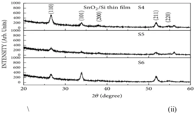
S3, after oxygen had streamed on the Si substrate for 1 h preceding the thin film was deposited. The (110), (211), and (101) planes of the thin films expanded in power as the development surface diminished. The thin film development by sputtering is
impacted by the power provided to the chamber. XRD tops are identified with the thickness of the thin film and the thickness of the thin film will change as the measure The surface of S1, S2, and S3 thin films developed at a testimony temperature of 350°C, an affidavit time of 1 h, an oxygen flow rate of 40 sccm, and provided powers of 100, 150, and 200 W. The thin films were
roundabout, and the molecule sizes
International Journal of Research
Available at https://edupediapublications.org/journalse-ISSN: 2348-6848 p-ISSN: 2348-795X Volume 05 Issue 19
August 2018
\ (ii)
Figure 1: X-beam diffraction patterns of the SnO2 thin films of S-1, S-2, and S-3 groups (an)
and S-4, S-5, and S-6 groups (b).
Further, the SiO2 layers deposited by
providing oxygen onto the Si substrate; the thin films were then shaped under indistinguishable conditions as those for S1, S2, and S3 thin films. The thin films are round, as on account of S1, S2, and S3 thin films and the molecule estimate increments with the provided control. Additionally
comprehension of microstructural
development could be accomplished
considering that the starting material displays auxiliary defects which, are identified with high oxygen vacancy focus.
Optical properties
The acquired transmittance and reflectance spectra from the optical examinations. It
International Journal of Research
Available at https://edupediapublications.org/journalse-ISSN: 2348-6848 p-ISSN: 2348-795X Volume 05 Issue 19
August 2018
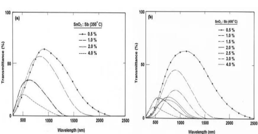
Figure 2: Transmittance spectra as a component of wavelength for SnO2 :Sb thin films
arranged at Ts of (a) 350 °C and (b) 400 °C separately
Figure 3: Reflectance spectra as an element of wavelength for SnO2 :Sb thin films arranged at
Ts of (a) 350 °C and (b) 400 °C separately
From the plot of reflectance spectra, it is under stood that the reflectance of the considerable number of films is very nearly zero till the wavelength of around 1500 nm for both substrate temperature. For the film
International Journal of Research
Available at https://edupediapublications.org/journalse-ISSN: 2348-6848 p-ISSN: 2348-795X Volume 05 Issue 19
August 2018
The films arranged at bring down substrate
temperature have marginally higher
reflectance esteems than those arranged at higher substrate temperature over the wavelength of ~1500 nm. The transmittance for the chose wavelengths of 600, 700, 800, and 900 nm are plotted against the capacity of Sb doping in the films arranged at lower
and higher substrate temperatures
individually.
It is obvious from the assume that for the films arranged at bring down temperatures the transmittance esteem at each chosen wavelength diminishes with expanding Sb doping focus. It was comprehended that as the doping builds, the rate of decline of transmittance of the higher wavelengths (800 and 900 nm) is higher than that of lower wavelengths (600 and 700 nm). As a result, the transmittance that demonstrated augmentation with expanding wavelength at bring down doping levels (< 2 wt. %) found to indicate decrement in transmittance with expanding wavelength at higher doping levels (> 2 wt. %). For the films arranged with higher substrate temperature, as the doping fixation increment, the transmittance
demonstrates a reliable decrement for the
higher wavelengths. Though the
transmittance for the lower wavelengths demonstrates a decrement till the Sb doping of 1.5 wt. % yet then demonstrates a slight increment.
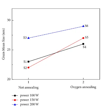
The average molecule sizes of S1– S6 films. The average molecule sizes of S1, S2, and S3 thin films are 23, 22, and 27 nm, individually. The average molecule sizes of S4, S5, and S6 thin films sintered in an oxygen climate are 26, 27, and 29 nm, individually. The average size dividing of S4, S5, and S6 films sintered in an oxygen air was not as much as that of S1– S3 films.
At the point when the SnO2 thin film is
developed after oxygen streams over the Si substrate, the average molecule size of the
SnO2 thin film is affected by the SiO2 layer,
International Journal of Research
Available at https://edupediapublications.org/journalse-ISSN: 2348-6848 p-ISSN: 2348-795X Volume 05 Issue 19
August 2018
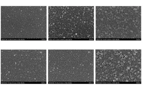
Figure 2:SEM pictures of the surface of the SnO2 thin films of S-1, S-2, and S-3 groups and S-4, S-5, and S-6 groups.
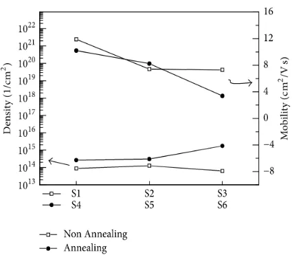
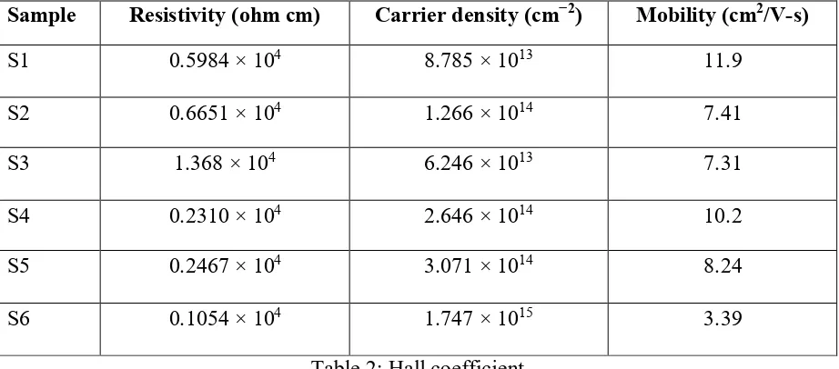
The versatility and surface charge thickness of the thin film acquired through the Hall estimation of thin films S1 to S6; the portability of S1– S6 was 11.9, 7.41, 7.31, 10.2, 8.24, and 3.39, separately. The versatility of the thin film diminished as the
provided control expanded, and it
diminished consistently when the power provided to thin films S4, S5, and S6 was expanded in the oxygen environment.
International Journal of Research
Available at https://edupediapublications.org/journalse-ISSN: 2348-6848 p-ISSN: 2348-795X Volume 05 Issue 19
August 2018
Figure 3: Mean grain size of the SnO2 thin films of S-1, S-2, and S-3 groups (1) and S-4, S-5,
and S-6 groups (2).
The surface charge densities of S4, S5, and S6 films sintered in the oxygen environment were 2.646 × 10¹⁴, 3.071 × 10¹⁴, and 1.747 × 10¹⁵, individually, and the vehicle charge
thickness of S4– S6 when an
indistinguishable power from that for S1– S3 was provided was marginally bigger than that of S1– S3. This is on account of the
SiO2 + SnO2 thin film shaped on the Si
substrate, and the carrier thickness expands on account of the bigger measure of oxygen
than that present in the unadulterated SnO2
thin film. It was affirmed that the force of provided control influences the surface
charge thickness and the portability of the
thin film and therefore that the SiO2 layer
between the Si substrate and the SnO2 thin
film influences the electrical properties of the thin film. By and large, the quick development rate of the thin film causes the poor electrical and optical properties because of the expansion of harshness and stick opening. In the abatement in portability and PL force in S3 and S6, which
have the biggest power amid film
International Journal of Research
Available at https://edupediapublications.org/journalse-ISSN: 2348-6848 p-ISSN: 2348-795X Volume 05 Issue 19
August 2018
Figure 4: Hall effect data of the SnO2 thin films.
The PL estimation of thin films S1– S6. The PL powers of S4, S5, and S6 films with SiO2 layer were not exactly those of S1, S2, and S3 films. On account of S4, S5, and S6 films, the discharge wavelengths of 431 nm and 444 nm (relating to S1– S3 films) moved to 434 nm and 415 nm, separately. The SnO2 thin film developed on the SiO2 layer has distinctive oxygen defects on
International Journal of Research
Available at https://edupediapublications.org/journalse-ISSN: 2348-6848 p-ISSN: 2348-795X Volume 05 Issue 19
August 2018
Figure 5: Photoluminescence spectra of the SnO2 thin films.
Sample Resistivity (ohm cm) Carrier density (cm−2) Mobility (cm2/V-s)
S1 0.5984 × 10⁴ 8.785 × 10¹³ 11.9
S2 0.6651 × 10⁴ 1.266 × 10¹⁴ 7.41
S3 1.368 × 10⁴ 6.246 × 10¹³ 7.31
S4 0.2310 × 10⁴ 2.646 × 10¹⁴ 10.2
S5 0.2467 × 10⁴ 3.071 × 10¹⁴ 8.24
S6 0.1054 × 10⁴ 1.747 × 10¹⁵ 3.39
Table 2: Hall coefficient
Conclusion
Thin films of antimony doped tin oxide thin films were set up by shower pyrolysis
strategy from SnCl2 antecedent at two
diverse substrate temperatures. The films arranged at higher substrate temperature indicated least sheet opposition. The base
sheet obstruction accomplished in the present investigation is the most reduced among the detailed qualities for these
materials arranged from SnCl2 forerunner.
International Journal of Research
Available at https://edupediapublications.org/journalse-ISSN: 2348-6848 p-ISSN: 2348-795X Volume 05 Issue 19
August 2018
focus. The films arranged at bring down substrate temperature demonstrated the most extreme transmittance. In the SnO2 thin films developed specifically on the Si substrate, the forces of (110) plane, (101) plane, and (211) plane showed a fortifying inclination to diminish. Be that as it may, in
SiO2+ SnO2 thin films, the (110), (101),
and (211) planes displayed an inclination to diminish gradually, and the development example of SnO2 thin films changed by the underlying creation condition of the thin film. The SEM pictures of the thin films
demonstrate that SnO2 thin films developed
specifically on the Si substrate had a huge normal molecule measure with expanding power force, and the normal molecule
estimate interim of the SnO2 thin films
developed on the SiO2 layer in the oxygen
climate was little. In the Hall impact estimation, the force of intensity provided to
the SnO2 thin film was influenced by the
surface charge thickness of the thin film, yet the thin film deposited by sintering in the oxygen air demonstrated the surface charge thickness.
It was affirmed that the SiO2 layer between
the substrate and the thin film influences the electrical properties of the thin film
inferable from the defects in the SnO2
surface and thin film. The optical properties
of the thin films developed
straightforwardly on the substrate were additionally not quite the same as those of
the SnO2 thin films developed on the
SiO2 layer by sintering in the oxygen
environment.
REFERENCE:
1. Malik, A. Seco, E. Fortunato, R.
Martins, J. Non Cryst. Solids 227-230, 1092 (1998).
2. J. Bruneaux, H. Cachet, M. Froment, A.
Messad, Thin Solid Films 197, 129 (1991).
3. C. Lozano, Ch. Comninellis, A. De
Battisti, J. Electrochem. Soc. 143, 203 (1996).
4. Stucki, R. Kotz, W. Suter, B. Carcer, J.
Appl. Electrochem. 21, 99 (1991).
5. E. Elangovan, K. Ramamurthi, J.
Optoelectron. Adv. Mater. 5, 45 (2003).
6. E. Elangovan, K. Ramamurthi,
Submitted in revised form to Cryst. Res. Technol., (2003)
7. G. Frank, E. Kauer, H. Kostlin, Thin
Solid Films 77, 107 (1981).
8. J. Jeong and B. J. Lee, “X-ray
photoelectron spectroscopy study of
SnO2 and SnO2 +x thin films,” Journal
of Nanoscience and Nanotechnology, vol. 13, no. 1, pp. 711–713, 2013.
9. S. Min and J. Jeong, “A study of
atypical grain growth properties for SnO2 thin films,” Materials Science in Semiconductor Processing, vol. 16, no. 5, pp. 1267–1270, 2013.
10. J. Jeong, “Effect of the Change of Deposition Time on the Secondary Direction and Abnormal Shape of
Grains Growth of SnO2 Thin
Films,” Advances in Materials Science and Engineering, vol. 2015, Article ID 350196, 2015.
11. Cirera, A. Comet, J. R. Morante, S. M. Olaizola, E. Castano, and J. Gracia, “Comparative structural study between
sputtered and liquid pyrolysis
International Journal of Research
Available at https://edupediapublications.org/journalse-ISSN: 2348-6848 p-ISSN: 2348-795X Volume 05 Issue 19
August 2018
Science and Engineering: B Advanced Functional Solid-State Materials, vol. 69-70, pp. 406–410, 2000.