Surface Wave Suppression in LHCP Microstrip Patch Antenna
embedded on Textured Pin Substrate
Manidipa Roy1, * and Ashok Mittal2
Abstract—Propagation of surface waves in dielectric underneath a microstrip patch antenna poses serious hindrance to the radiation mechanism. Several methods are being tried for suppression of surface wave. Metamaterial substrate is presented here with periodic arrangement of metallic cylindrical pins except the area underneath the radiating microstrip patch. The periodic arrangement of metallic cylindrical pins with negative dielectric constant has considerably high reflection coefficient to drive the extraneous surface wave fields towards the fringing fields of the antenna. The textured pin substrate leads to generation of forbidden band gap for the propagation of TM0 surface wave modes and thus enhances radiation characteristics. The proposed structure proves to be highly beneficial for improving radiation efficiency and gain. Parametric analysis has also been presented for the gain enhancement by varying pin diameter, spacing between pins, and air gap between dielectric substrates. A uniform gain of 10 dB has been achieved for a Left Hand Circularly Polarized (LHCP) microstrip patch antenna. The axial ratio achieved in the described band is 200 MHz. The antenna has been designed for WLAN applications.
1. INTRODUCTION
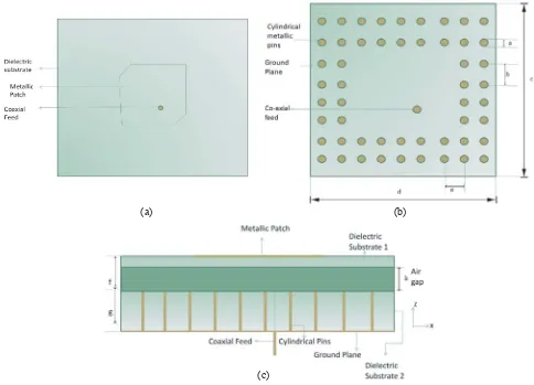
Microstrip patch antennas are widely employed for wireless and space borne applications because of their planar geometry, ease of fabrication, light weight and low cost [1–3]. Achieving circular polarization is one of the most important features in the antennas as the electromagnetic wave is affected by distance with Faraday’s rotation and geometric differences at different locations. Circular polarization in microstrip patch antennas [1, 2] has been achieved either by using dual feed antennas (with orthogonal feeds) or by perturbing the patch at specific locations. In this paper microstrip patch antenna is designed, for achieving circular polarization with chamfered edges, on one of the diagonal corners (see Fig. 1(a)).
Secondly, the planar microstrip patch antennas have several drawbacks such as low gain, low radiation efficiency and low front to back ratio (FBR). Predominantly the reason is propagation of surface wave modes. The dominant TM0 surface wave mode propagates beneath the patch surface and gets radiated from the edges of the dielectric. This proves to be the hindrance to radiation characteristics of the antenna as the power is lost due to leakage from the edges. The surface wave propagation can be controlled by micromachining technology [4]. The portion of substrate beneath the patch antenna is etched out by micromachining. Other techniques used for the control of surface waves are by use of meta surfaces [5]. A periodic arrangement of regular pattern is etched as the radiating surface on the dielectric.
The propagation of surface wave mode can also be suppressed by designing an artificial dielectric substrate. The artificial dielectric substrate is designed with periodic arrangement of metallic vias inserted in a dielectric substrate. The metallic vias embedded in the dielectric substrate (Fakir’s bed of
Received 28 July 2018, Accepted 18 December 2018, Scheduled 3 January 2019
* Corresponding author: Manidipa Roy ([email protected]).
(a) (b)
(c)
Figure 1. Geometry of a circularly polarized rectangular patch embedded on the textured surface formed by a square grid of metallic pins embedded in dielectric substrate (FR4 Epoxy). (a) Top view. (b) Bottom view. (c) Side view.
nails) prove to act as an Electromagnetic Band Gap (EBG) Structure. EBG substrates are designed in such a way that they provide band gap characteristics to the propagation of surface wave modes. The periodic arrangement of cylindrical metallic pins proves to provide negative permittivity to the dielectric substrate [6, 7]. Nikoli´c et al. [8] proposed that the number of pins and the spacing between them are selected such that the inductive currents on the pins cancel out the capacitive substrate polarization. The study of surface wave propagation and methods to eliminate it are illustrated in research papers by King et al. [9], Sievenpiper et al. [10], Silverinha et al. [11].
The periodic arrangement of metallic vias inserted throughout the dielectric substrate runs through the resonant cavity of the radiating structure as well. This affects the radiation characteristics. To overcome the problem, the grid of periodic metallic vias is removed from the surface underneath the radiating structure (see Fig. 1). Thus the artificial dielectric incorporated has high impedance and is capacitive in nature. The surface waves experience attenuation due to this high impedance surface, thus this medium serves the function of focusing the radiation in the desired direction. This boosts the radiation and reduces losses due to surface waves.
2. THEORY OF SURFACE WAVES
Surface waves are characterized as the waves that attenuate in nature and propagate in the transverse direction to the antenna plane. The surface wave propagates in dielectric with permittivity greater than 1. The surface waves generate from the part of fringing fields entering the dielectric with angle of incidence lying in range ofπ/2 to sin−1(1/√εr). The conventional grounded substrate antenna structure supports TM surface wave modes. The lowest order TM mode that has no cutoff frequency is TM0 mode.
Microstrip antennas have narrow bandwidth. Bandwidth is improved with the use of thicker substrates. As the substrate thickness increases, surface waves get excited, and the antenna gain is reduced and the radiation efficiency degraded. Reduction of surface waves can be done by using parasitic elements next to the radiating edges. The parasitic elements reflect the surface waves back to the microstrip cavity and enhance the radiation characteristics. A part of it is reflected and radiates as space waves, and the rest goes back into the resonating cavity. These returned waves form a standing wave and create an extra mode in the cavity. As a result, the resonant resistance will increase. The extra mode created by surface mode excitation has a similar field distribution to dominant mode. The power carried by surface waves is considered as loss because it is trapped in the dielectric substrate. Moreover, unwanted radiation occurs when the surface wave encounters a discontinuity, i.e., at the edge of substrate.
3. ANALYSIS OF SURFACE WAVE MODE
A simple square microstrip patch antenna is designed at 5.45 GHz for WLAN applications. The circular polarization has been achieved by chamfering the edges, on one of the diagonal corners of the square patch. The structure has been simulated using Ansoft HFSS. The results show axial ratio around 1 dB, but the gain and radiation efficiency are observed very low. The degradation of these parameters is due to propagation of surface waves. The TM0 surface wave mode gets excited very easily as it has very low cutoff frequency.
Because TM0 mode has zero cutoff frequency, it will always be excited at the open end of the microstrip antenna. It will even propagate on very thin substrates having low dielectric constant values at nearly the velocity of light.
For TM0 mode in lossless substrates, the radial propagation constant β is real [1] and is bounded by
1< β/k0 < εh (1)
wherek0 is the free space wave number.
If the substrate is electrically thin, β/k0 = 1. The value of β/k0 can be obtained by assuming
β/k0 = 1 +δ, whereδ is the loss tangent β/k0 coming out to be 1.09 approximately, which lies in the range 1< β/k0 < εh, thus it is postulated from this result that TM0 surface wave mode propagates.
The approximate expression forβ is, [11]
βr = β (2)
βi = (εh−1) tanδ(k0h/εh)2 (3)
Using these relations, β comes out to be
β = 81.69 +j0.0034, and k0 is 83.73.
The result signifies that the substrate is electrically thin, becauseβ/k0 approaches 1 (the value of k0) which again confirms the presence of TM0 mode propagation in the substrate.
For the single-layer substrate n= 1, [1]
h/λ0 <1/4 √
(εh−1) (4)
So, according to the design of the proposed structure,h <32.6 mm. For multi-layer substrate the value of β/k0,
β/k0 = 1 + 1 2
N i=1
εri−1
εri k0hi
2
where εri and hi are the constituent parameters of theith layer with N as the number of layers. This relation holds good for the antenna structure considered upon.
The consistency of the substrate thickness with above relationship signifies that only TM0 mode propagates, and all other modes are below cutoff.
The space wave efficiency [11]
η= Psp Psp+Psw
(6)
wherePsp= space wave power, and Psw = surface wave power.
The space wave efficiency comes out as 42% using the above equation. The space wave efficiency can be improved using a high dielectric substrate. The artificial dielectric substrate with negative permittivity can be designed using an array of shorting pins embedded in the dielectric substrate. Consequently, the suppression of surface waves is done by using an array of metallic pins embedded around the patch antenna. The change in effective dielectric constant is desirable for this purpose of inhibiting the propagation of surface waves.
4. DESIGN OF TEXTURED PIN SUBSTRATE
TM0 surface wave mode propagates in the direction transverse to that of the antenna plane. Thus to seize its propagation, discontinuity has to be introduced to its flow in the same direction. The substrate is embedded with cylindrical pins in longitudinal direction which are placed in a square grid manner throughout the substrate except below the patch antenna as shown in Fig. 1. The artificial dielectric incorporated in this way is with high impedance and is capacitive in nature, and the surface waves experience attenuation due to this high impedance surface. The medium serves the function of focusing the radiation in the desired direction. This boosts the radiation and reduces losses due to surface waves. The dielectric medium now becomes anisotropic and acts as an artificial dielectric medium. Design equations using the theory of artificial dielectrics and propagation in anisotropic media are given in [1, 2, 6, 7, 13, 14]. The dielectric constant and relative permeability tensors are
[ε] =
ε
x 0 0
0 εy 0 0 0 εz
[μ] =
μ
x 0 0
0 μy 0 0 0 μz
(7)
When the cylindrical wires are z-directed, the electric field is in z-direction and magnetic field in y-direction.
The refractive index of such a medium is,
ηzy= (εzμy/εdμd)1/2 (8)
can be found using the relation
cos (ηzyθ) = cosθ+A/θsinθ (9)
whereθ=kdeis the electrical spacing, andkd is the wave number in the dielectric medium and
A= πe
(bln(b/π)). (10)
The cylinder spacings in the x- and y-directions are ‘e’ and ‘b’, respectively, (for selected square grid ‘e’ will be equal to ‘b’), and ‘a’ is the cylinder diameter. Hereεd,μdare the dielectric constant and relative permeability, respectively. This theory is only valid if
aeλd/2 (11)
whereλd is the artificial dielectric medium wavelength.
The wave will propagate only if the refractive indexnzy is real, i.e.,
−1<cos (ηzyθ)<1 (12)
resonant frequency of the patch antenna. A square patch antenna is designed at 5.45 GHz for WLAN applications.
The textured pin substrate as shown in Fig. 1(b) is designed with cylindrical pins of diameter a = 1 mm and lattice spacing e = b = 1 mm. For achieving circular polarization, the two diagonal edges have been chamfered as shown in Fig. 1(a), and the chamfered areas from the diagonal corners are 0.67 m2 and 0.689 m2. The top most dielectric substrate is FR4 Epoxy with thickness 0.4 mm; the air gap ‘h’ is chosen as 0.4 mm from parametric analysis; the textured pin substrate is again FR4 Epoxy with thickness 1.6 mm.
5. PARAMETRIC ANALYSIS
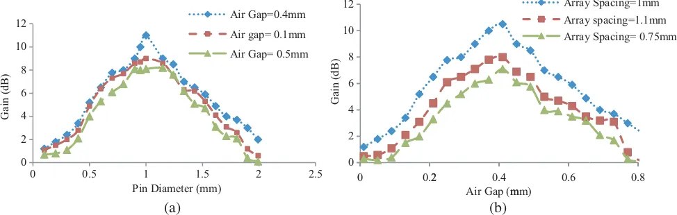
Parametric analysis has been carried out with pin diameter ‘a’, array spacing ‘b’, air gap ‘h’. For optimizing gain, parametric analysis is carried out by varying the pin diameter ‘a’ from 0.1 mm to 0.5 mm, keeping the array spacing ‘b = 1 mm. The optimum value of the air gap is 0.4 mm, and pin diameter is 1 mm with maximum gain of 11 dB as shown in Fig. 2(a). Fig. 2(b) gives gain optimization by varying the air gap ‘h’ from 0.75 mm to 1.1 mm, keeping the pin diameter ‘a = 1 mm constant. The optimum value of the air gap is 0.4 mm, and array spacing is 1 mm with maximum gain of 10 dB.
0 2 4 6 8 10 12
0
0 0.22 0.4
Air Gap (m
0.6 Array Array Array
mm)
0.8 y Spacing=1mm y spacing=1.1mm
y Spacing= 0.75mmm
Gain
(dB)
0 2 4 6 8 10 12
0 0.5 1 1.5 2 2.5
Air Gap=0.4mm
Air gap= 0.1mm
Air Gap= 0.5mm
Gain
(dB)
Pin Diameter (mm)
(a) (b)
Figure 2. (a) Gain Optimization by varying the pin diameter ‘a’ (keeping Array Spacing ‘b = 1 mm). (b) Gain Optimization by varying the Air gap ‘h’ (keeping Pin Diameter ‘a= 1 mm).
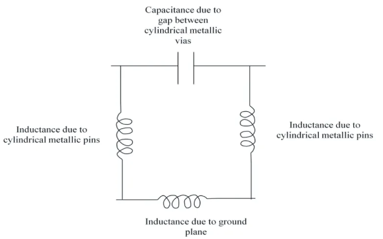
6. EQUIVALENT CIRCUIT MODEL OF EMBEDDED PIN BED STRUCTURE
Equivalent Circuit Model technique has been used for analyzing the structure. The microstrip patch antenna surface is divided into a number of square patches of very small size, then each patch sub part and the ground plane form a parallel plate capacitor (see Fig. 3). The capacitance of the capacitor is calculated by using the formula [1, 12]
C =εrεhS
h =C0+Cd (13)
whereC0 is the capacitance with the portion of substrate removed
C0=ε0hS (14)
and Cdis the capacitance due to the presence of dielectric
Cd=
(εr−1)εhS
h . (15)
Figure 3. Equivalent circuit model of a single section of textured pin substrate (for a single cylindrical metallic pin).
followed here,ω2LCd= 1. For simplicity if the area of square is replaced by area of circle, then πb2=S. Assuming that the polarization currents are uniformly distributed along the patch, the inductance of the pin is given by the following relation [1]
L=μ0
2π(lnb/a−3/4)h. (16)
An array of shorting pins is embedded beneath patch and the ground plane to introduce inductive currents of the metallic pins, which nullifies the polarization currents of the capacitor.
7. SUPPRESSION OF SURFACE WAVES USING TEXTURED PIN SUBSTRATE
Figure 1 shows the textured surfaces with embedded wire medium. The array of metallic pins embedded in the dielectric substrate or the textured pin substrate is used to change the surface impedance.
The dielectric constant of the metallic pins is
εmetal= 1+jωεσ
0
= 1+ 2
j(βδskin)2 (17)
whereδskin≈2/μ0σω is the skin depth of the metal andβ =ω/c. The effective dielectric constant for the wire medium is
εzz(ω,kZ) = 1 +
1
εh
εmetal−εhfv−
β2
h−k2Z
β2
p
(18)
wherefv =π(a/2∗e)2 is the volume fraction of the rods.
The value of εmetal = 1−j0.02 × 1010, and the value of ε
zz(ω,kZ) = −1.21 − j0.001 using
Equation (16).
Thus the value ofεeff, i.e.,
εeff =ε0εh(ˆuxuˆx+ ˆuyuˆy+εzz(ω, kz) ˆuzuˆz)
εeff = 38.96×10¹²(0.79−j0.001).
where εh is the relative permittivity of the host medium, βh = β√εh the wave number in the host material, β = k0 = ω/c the wave number in free space, kz the z-component of the wave vector
k = (kx, ky, kz) of the plane wave, and βp the plasma wave number, which only depends on the geometrical properties of the lattice
(βpa)2= 2π ln
a 2πrw
+ 0.5275
. (20)
The dispersion characteristic of TM mode supported by the wire medium is β2
h=βp2+k2 (21)
wherek2 =k·k.
The reflection coefficient can be represented as,
ρ= −
βhβ2ptan (βhL)−k2γTMtanh (γTML) +εhγ0
β2+k2
βhβp2tan (βhL)−k2γTMtanh(γTML)−εhγ0
β2+k2
(22)
where k = (kx, ky,0) is the component of wave vector parallel to the interface (for propagating wave k = βsinθ, where β = ω/c, θ is the angle of incidence, and γ0 and γTM are the free space and TM mode propagation constants). The value of reflection coefficient comes out to be 0.11−j0.99.
For the densely packed wires surface impedance,Zs, is,
Zs= jη0tan(√ βhL) εh
(23)
The dense array of wires may be characterized by the impedance boundary. TM-surface wave modes propagate whenZsis inductive, and are suppressed whenZsis capacitive. The value ofZsis−j54.08 Ω which is capacitive, and this signifies the suppression of TM-surface wave modes.
The poles of reflection coefficient, ρ, correspond to the surface wave modes. Thus, a surface wave mode has wave numberk =k(ω) verified
βhβp22 tan (βhL)
β2+k2
−k 2
γTMtanh (γTML)
β2+k2
−εhγ0= 0 (24)
where bothγ0 and γTM are functions of frequency.
8. VALIDATION OF RESULTS USING REDUCED SURFACE WAVE THEOREM
The structure proposed here uses a proper choice of filling substrate material inside the patch cavity, i.e., between the patch and the ground plane. This does not require any special geometry for the microstrip as long as the element is planar in geometry. By properly selecting the substrate material and the permittivity of the substrate filling material, it is possible to eliminate the excitation of the dominant surface wave by an arbitrarily shaped patch, when it is operating at resonance. The reduced surface wave theorem [4] states that the surface wave propagation decreases if the dielectric constant of the substrate in the patch cavity is chosen to be
εreff=
βTM0
k0 2
(25)
9. RESULTS
The proposed antenna using a textured pin substrate in multilayer configuration exhibits improved radiation characteristics and superior matching characteristics. Fig. 4 shows the return loss characteristics of the simulated and measured results at the design frequency 5.45 GHz.
-25 -20 -15 -10 -5 0
5.15
S1
1 (dB)
5.35 F
5.55 Frequency (GHz)
5.75 Simulat Measur
5 ted result red result
Figure 4. Simulation and measured plot showingS11characteristics.
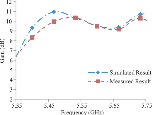
The improvement in gain characteristics as being observed is shown in Fig. 5.
2 3 4 5 6 7 8 9 10 11 12
5.35 5.45 5.55 5.65 5.75
Simulated Result Measured Result
Ga
in
(dB
)
Frequency (GHz)
Figure 5. Simulation and measured plot showing Gain characteristics.
The axial ratio graph in Fig. 6 is plotted which supports circularly polarized radiation. The simulation results are compared with the measured ones. The axial ratio characteristics show that 200 MHz axial ratio bandwidth is achieved.
0 0.2 0.4 0.6 0.8 1 1.2 1.4 1.6 1.8 2
5.25 5.35 5.45 5.55 5.65
Simulated result
Measured result
A
x
ia
l r
ati
o (
d
B)
Frequency (GHz)
Figure 6. Simulation and measured plot showing axial ratio characteristics.
4 6 8
10
90 60 30 0
-30
-60
-90
-120
-150
-180
150 120
Radiation Pattern –Gain (dB)
Antenna embedded on simple dielectric substrate Antenna embedded on Multi-layered textured dielectric substrate
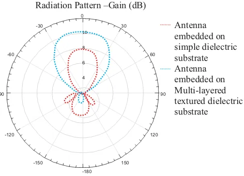
Figure 7. Radiation pattern showing Gain characteristics.
10. CONCLUSION
A multi-layer structure with metallic vias inserted throughout a dielectric substrate but removed underneath the radiating printed patch antenna has been presented. The periodic arrangement of metallic cylindrical pins with negative dielectric constant offers considerably high reflection coefficient to drive extraneous surface waves towards the fringing fields of the antenna. The textured pin substrate leads to generation of forbidden band gap for the propagation of TM0 surface wave modes and thus enhances radiation characteristics. The proposed structure proves to be highly beneficial for improving radiation efficiency and gain. A uniform gain of 10 dB has been achieved for a Left Hand Circularly Polarized (LHCP) microstrip patch antenna. The antenna has been designed for WLAN applications.
REFERENCES
4. Komanduri, V. R., D. R. Jackson, J. T. Williams, and A. R. Mehrotra, “A general method for designing reduced surface wave microstrip antennas,” IEEE Transactions on Antennas and Propagation, Vol. 61, No. 6, 2887–2894, June 2013.
5. Xu, H.-X., G.-M. Wang, J.-G. Liang, M. Q. Qi, and X. Gao, “Compact circularly polarized antennas combining meta-surfaces and strong space-filling meta-resonators,” IEEE Transactions on Antennas and Propagation, Vol. 61, No. 7, 3442–3450, July 2013.
6. Brown, J., “Artificial dielectrics having refractive indices less than unity,”Proc. IEE, Radio Section, 11–23, Monograph. 62, 1953.
7. Rotman, W., “Plasma simulation by artificial dielectrics and parallel plate media,” IRE Transactions on Antennas and Propagation, 81–96, January 1961.
8. Nikoli´c, M. M., A. R. Djordjevi´c, and A. Nehorai, “Microstrip antennas with suppressed radiation in horizontal directions and reduced coupling,”IEEE Transactions on Antennas and Propagation, Vol. 53, No. 11, 3469–3476, November 2005.
9. King, R. J., D. V. Thiel, and K. S. Park, “The synthesis of surface reactance using an artificial dielectric,” IEEE Transactions on Antennas and Propagation, Vol. 31, No. 3, 471–476, May 1983. 10. Sievenpiper, D., L. Zhang, and R. F. J. Broas, “High impedance electromagnetic surfaces with a forbidden frequency band,” IEEE Transactions on Antennas and Propagation, Vol. 47, No. 11, 2059–2074, November 1999.
11. Silveirinha, M. G., C. A. Fernandes, and J. R. Costa, “Electromagnetic characterization of textured surfaces using textured Pins,” IEEE Transactions on Antennas and Propagation, Vol. 56, No. 2, 405–415, February 2008.
12. Carver, K. R. and J. W. Mink, “Microstrip antenna technology,” IEEE Transactions on Antennas and Propagation, Vol. 29, No. 1, 2–24, January 1981.
13. Pozar, D. M., “Rigorous closed form expressions for the surface wave loss of printed antennas,” Electronic Letters, Vol. 26, No. 13, 954–956, June 1990.