Wide Band L-Probe Fed Circular Patch Antenna with Elliptical
Parasitic Patch and Two Elements Array
Muhammad N. Islam1, 2, *, Markus Berg2, Timo Tarvainen1, and Erkki T. Salonen2
Abstract—To enable the quest for high data rates in telecommunications, wide-band radio designs as well as antennas are required. This paper demonstrates a unique bandwidth enhancement technique for L-probe fed patch antenna. This is a novel technique to enhance patch antenna bandwidth with desired radiation properties. One circular shape main patch and two elliptical shape parasitic patches on PCB give wide-band response by exciting multiple resonances. The designed antenna array gives almost 45%,
−10 dB impedance matched relative bandwidth. This is a very simple and inexpensive patch antenna solution for the wide-band wireless application. A two-element array of this antenna has been formed, and wide-band radiation properties of the array are reported.
1. INTRODUCTION
Wide-band solution in antenna design is becoming more challenging as the number of bands used in the world is increasing. For base station antenna design, it becomes more complex as manufacturers tend to prefer one antenna solution for worldwide products. The antenna is one of the biggest parts of the base station head unit. The most challenging case is the lower part of operating bands of the E-UTRA system, as lower frequency means larger antenna. According to 3GPP E-UTRA operating bands standard [1], lower part of frequencies, which are partially implemented and going to implement worldwide in the future, ranges from 698 MHz to 960 MHz. For an antenna designer, the main challenge is to find an antenna solution which will cover low-band frequencies that satisfies typical radiation properties of a directional base station antenna.
Widening bandwidth of a patch antenna has been done in many ways. Typically parasitic patch and L-probe feeding have become the popular techniques for wide-band solutions. An analysis of L-probe-fed technique is described in [2, 3]. A dual-band dual-fed L-probe patch antenna has been reported in [4]. In those papers mainly the L-shaped probe structure and its working principle have been described in detail. Bandwidth increase by parasitic patch has been reported in [5, 6]. Capacitive fed technique, which is used to increase GPS antenna bandwidth, has been described in [7]. L-probe fed circular patch antenna with 30% bandwidth (VSWR≤2) is reported in [8] and has conical shape radiation patterns. Circular patch antenna mode excitation, substrate height, dielectric properties and ground plane effects have been studied in [9]. Some articles [10–13] have reported different patch shapes and patch alteration methods to increase bandwidth. A U-shaped slot wide-band patch antenna with 47% bandwidth (VSWR
≤2) and asymmetric radiation patterns in two planes is presented in [10]. However, wide-band radiation properties have not been reported in that article. Multiple U-slots and V-slots for multiple narrow band resonances with L-probe fed antenna are reported in [11]. An L-probe fed H-shaped patch antenna with 22.63% bandwidth at 10 dB return loss is presented in [12]. A direct fed wide-band E-shaped patch antenna design with 30% bandwidth at 10 dB return loss and analysis of multiband E-shaped direct fed patch antenna have been discussed in [13, 14]. The ground plane size effect on antenna properties
Received 20 October 2015, Accepted 11 December 2015, Scheduled 22 December 2015 * Corresponding author: Muhammad Nazrul Islam ([email protected]).
simulation tool has been used to calculate antenna properties. Calculated results are validated by building the model and measuring antenna properties.
2. DESIGN PROCEDURE
2.1. Design of a Wide-Band L-Probe Fed Patch Antenna by Main and Parasitic Patch Shapes
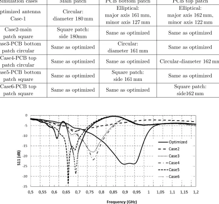
Design focus was to design an antenna suitable for all E-UTRA low bands (699 MHz to 960 MHz). After many trials, an adequate broad band L-probe fed patch antenna structure was found. This antenna has one main patch and two parasitic patches. Parasitic patches are on a PCB’s top and bottom layers. Design goal was to achieve broad band response by patch shape, patch dimensions and patch combinations. Patch shape and dimension optimizations were done by trial and error as trial and error process is a common practice in most patch antenna design. An optimized L-probe fed patch antenna with 100 ohm input impedance was found.
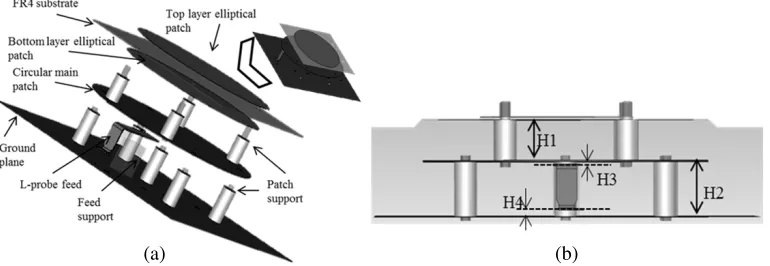
This optimized L-probe fed patch antenna has a circular shape main patch close to L-probe fed and two elliptical shape patches on a PCB’s top and bottom layers. An elevated single element antenna structure and its different parts are shown in Fig. 1. The circular patch is a 1 mm thick brass metal plate, and PCB patches are 30µm thick two-layered elliptical shape copper on a 1.5 mm thick FR4 substrate. The spacing between L-probe and main patch and spacing between main patch and PCB were chosen by iteration. In this optimization process, manufacturing compatibility has been factored in. An optimized combination of patches and their shapes provide multiple resonances and give a wide-band solution. For the right spacing between patches and L-probe, plastic screws support has been used. These screws also assist to adjust the height properly. All the spacing is shown in Fig. 1. L-probe was supported with foam to the ground plate. This foam has approximate air dielectric properties. The detailed dimensions of the circular metal patch and PCB elliptical patches are shown in Fig. 2.
L-probe feeding structure and its relative position from circular patch center are shown in Fig. 3.
(a) (b)
(a) (b) (c)
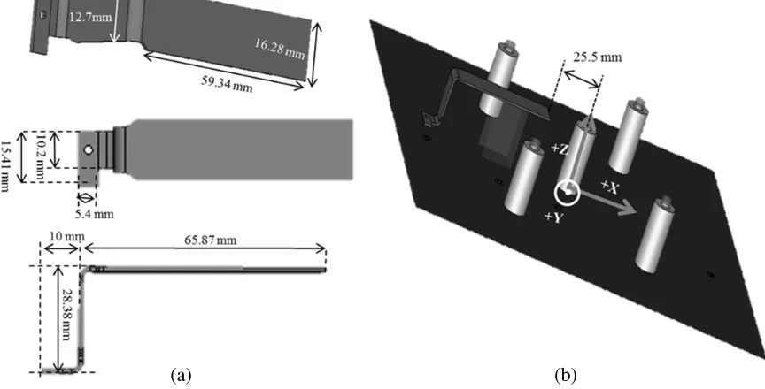
Figure 2. (a) Circular main patch. (b) Elliptical patch on PCB top. (c) Elliptical patch on PCB bottom.
(a) (b)
Figure 3. (a) L-probe fed structure. (b) Circular patch center and L-probe edge spacing.
L-probe fed top part is aligned to the circular patch diagonal. According to this figure, it is clear that this antenna has been designed forX direction polarization. End of the L-probe bottom part has been connected to the antenna array feeding network in a two-element array design. 1 mm thick copper metal is used in this feed line design.
patch square side 180mm Case3-PCB bottom
patch circular Same as optimized
Circular:
diameter 161 mm Same as optimized
Case4-PCB top
patch circular Same as optimized Same as optimized Circular-diameter 162 mm Case5-PCB bottom
patch square Same as optimized
Square patch:
side 161 mm Same as optimized
Case6-PCB top
patch square Same as optimized Same as optimized
Square patch: side162 mm
Figure 4. Simulated reflection coefficients for different patch shape combinations defined in Table 1.
2.2. Two-Element Array
In the two-element array design, 0.7λ(at 830 MHz) spacing between the antennas is used. After getting a suitable antenna element and right spacing for the two-element array, one corporate feeding network was designed. Each end of the feeding network is connected to an L-probe fed end. As each element has 100 ohm input impedance, a separate impedance transformer was not needed in its fed network design. In this two-element combiner, T-junction natural output comes as 50 ohm input impedance. Fig. 6 shows major dimension of the feeding network. The gap between ground and 100 ohm strip line is 4 mm. In 50 ohm strip line, this gap is 2 mm. In this fed lines design, strip line turn truncation and T-junction tapering has been optimized for impedance matching and less loss. This T-junction combiner and transmission line can be designed with different ground spacings and strip line widths.
Figure 6. Fed combiner for two-element array and L-probe fed structure.
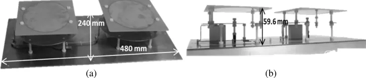
A two-element antenna array has been manufactured to examine its array performance for wide frequency range. The manufactured antenna array is shown in Fig. 7. This array is built on 240 mm width and 480 mm long ground plane. All plastic screws gaps are adjusted to the height of the simulation model. The screws on the trace line make this structure quite stable on the ground plane. Spacings between traces and ground plane are maintained by small plastic bushing, which has less effect on transmission line properties.
(a) (b)
Figure 7. (a) Two-element array structure. (b) Patch and fed line fixing mechanics.
3. PERFORMANCE
Figure 8. Measured and simulated reflection coefficients for the two-element array.
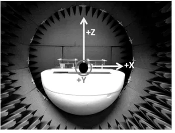
Figure 9. Antenna array placement in the measurement chamber.
Antenna array radiation properties have been measured in the near-field measurement system (SatimoStarLab) at the Department of Communications Engineering, University of Oulu. This antenna ground plane (48 cm) is slightly larger than the maximum guaranteed size (40 cm) of the DUT in which particular chamber and measurement accuracy below 800 MHz is not recommended. The chamber was calibrated from 700 MHz. Despite this limitation, the antenna array has been measured from 700 MHz to 1000 MHz. This measurement gives us measured and calculated values for comparative validation particularly above 800 MHz.
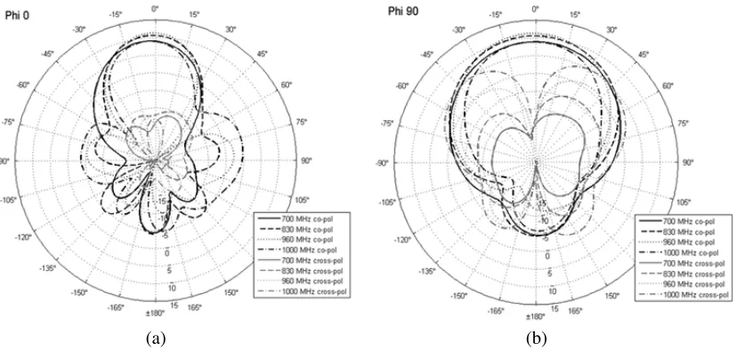
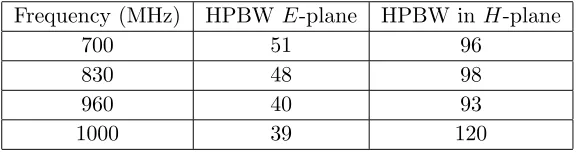
The near-field antenna measurement chamber’s coordinate system and the antenna placement in the chamber are shown in Fig. 9. From this coordinate system and antenna placement in it, we can find elevation (XZ plane or E plane) and azimuth (Y Z plane or H plane) antenna patterns. Fig. 10 presents both simulated and measured total radiation efficiencies. From efficiency plot, it is evident that this antenna array radiates efficiently at its resonance frequencies. There is a small discrepancy between measurement and simulation, and it is more prominent below 800 MHz. Part of this comes from inaccurate chamber below 800 MHz
The antenna array maximum gains, both from measurement and simulation are plotted in Fig. 11. The simulation and measurement correlate well. The max gain varies from 9 dBi to 11.49 dBi within the whole bandwidth. Lower frequencies have slightly lower max gain than the max gain at the frequencies of 850 MHz to 960 MHz.
Figure 10. Measured and simulated total efficiency for antenna array.
Figure 11. Measured and simulated maximum gains for the two-element array.
(a) (b)
4. CONCLUSION
A unique wide-band patch antenna design and an array of two elements of this antenna is found and validated by proto build and measurement. A consistent array performance across the band shows that this design concept is a good candidate for wide-band high gain patch antenna array design. From this calculation and measurement it is found that by choosing appropriate patch shapes and their combination, it is possible to get a very wide-band response in L-probe feed technique. Such relative bandwidth (45%) patch antenna array has not been found before, as far as we know. Further tuning of reflection coefficient and optimization over the desire frequency band can be done in feeding network, patches and height. Reducing overall height of the antenna and making this design as low profile design could be a future design task. In addition to this, a dual-polarized wide-band solution can be tried out for future study.
ACKNOWLEDGMENT
The first author, Muhammad Nazrul Islam, would like to thank Oulu University workshop and Kai Schr¨oder from Esju Oy.
REFERENCES
1. E-UTRA operating bands, 3GPP TS 36.101 Var 10.10.0 [Online]. Available:
http://www.3gpp.org/ftp/Specs/2013-03/Rel-10/36 series/.
2. Guo, Y. X., K. M. Luk, and K.-F. Lee, “L-Probe fed thick-substrate patch antenna mounted on a finite ground plane,” IEEE Trans. Antennas and Propagation, Vol. 21, No. 21, 1955–1963, Aug. 2003.
3. Guo, Y.-X., C.-L. Mak, and K.-M. Luk, “Analysis and design of L-probe proximity fed patch antenna,” IEEE Trans. Antennas and Propagation, Vol. 49, No. 2, 145–149, Feb. 2003.
4. Li, P., K. M. Luk, and K. L. Lau, “A dual-feed dual-band L-probe patch antenna,” IEEE Trans. Antennas and Propagation, Vol. 53, No. 7, 2321–2323, Jul. 2005.
5. Lee, R. Q. and J. Bobinchak, “Characteristics of a two-layer electromagnetically coupled rectangular patch antenna,” Electronics Letters, Vol. 23, No. 20, 24, Sep. 1987.
6. Wood, C., “Improved bandwidth of microstrip antennas using parasitic elements,” IEE Proc., Vol. 127, Pt. H, No. 4, Aug. 1980.
7. Islam, M. N., S. I. Karhu, and E. T. Salonen, “GPS and GSM antenna with a capacitive feed for a personal navigator device,” Wireless Information Technology and Systems (ICWITS), 2010. 8. Guo, Y. X., K. M. M.W. Chia, Z. N. Chen, and K.-M. Luk, “Wide-band L-probe fed circular patch
antenna for conical-pattern radiation,” IEEE Trans. Antennas and Propagation, Vol. 52, No. 4, 1115–1116, Apr. 2004.
10. Huynh, T. and K. F. Lee, “Single-layer single-patch wideband microstrip antenna,” Electronics Letters, Vol. 31, No. 16, 1310–1312, Aug. 1995.
11. Salamat, C. D., M. Haneishi, and Y. Kimura, “L-probe fed multiband microstrip antennas with slots,”Proseeding of Asia-Pacific Microwave Conference, 2006.
12. Ali, M. T., N. Nordin, I. Pasya, and M. N. Md Tan, “H-shaped microstrip patch antenna using L-probe fed for wide-band application,” 6th European Conference on Antenna and Propagation, Mar. 26–30, 2012.
13. Yang, F., X.-X. Zhang, X. Ye, and Y. Rahmat-Samii, “Wide-band E-shaped patch antennas for wireless communications,”IEEE Trans. Antennas and Propagation, Vol. 49, No. 7, 1094–1100, Jul. 2001.
14. Jin, N. and Y. Rahmat-Samii, “Parallel particle swarm optimization and finite-difference time-domain (PSO/FDTD) algorithm for multiband and wide-band patch antenna designs,” IEEE Trans. Antennas and Propagation, Vol. 53, No. 11, 3459–3468, Nov. 2005.
15. Bhattacharyya, A. K., “Effects of finite ground plane on the radiation characteristics of a circular patch antenna,” IEEE Trans. Antennas and Propagation, Vol. 38, 152–159, Feb. 1990.
16. Lier, E. and K. R. Jakobsen, “Rectangular microstrip patch antennas with infinite and finite ground plane dimensions,”IEEE Trans. Antennas and Propagation, Vol. 31, No. 7, 978–984, Nov. 1983. 17. Lo, W. K., K. M. Shum, C. H. Chan, and K. M. Luk, “Wide-band L-probe fed base-station antenna