Volume 2006, Article ID 41898, Pages1–10 DOI 10.1155/ASP/2006/41898
Analogue MIMO Detection
Robert J. Piechocki,1Jose Soler-Garrido,1Darren McNamara,2and Joe McGeehan1, 2
1Centre for Communications Research, University of Bristol, Merchant Venturers Building, Woodland Road, Bristol BS8 1UB, UK 2Telecommunications Research Laboratory, Toshiba Research Europe Ltd, 32 Queen Square, Bristol BS1 4ND, UK
Received 1 December 2004; Revised 17 May 2005; Accepted 8 July 2005
In this contribution we propose an analogue receiver that can perform turbo detection in MIMO systems. We present the case for a receiver that is built from nonlinear analogue devices, which perform detection in a “free-flow” network (no notion of iterations). This contribution can be viewed as an extension of analogue turbo decoder concepts to include MIMO detection. These first analogue implementations report reductions of few orders of magnitude in the number of required transistors and in consumed energy, and the same order of improvement in processing speed. It is anticipated that such analogue MIMO decoder could bring about the same advantages, when compared to traditional digital implementations.
Copyright © 2006 Hindawi Publishing Corporation. All rights reserved.
1. INTRODUCTION
Turbo codes and more general turbo principles (turbo equal-isation, turbo multiuser detection, etc.) are bound to have a substantial impact on the next-generation wireless systems. The turbo principle requires exchange of the so-called soft information, which is a probabilistic measure. In current implementations (e.g., turbo coding) this information is sampled then quantised (digitised) and handled by digital signal processors. The amount of digital information to be processed by DSPs and FPGAs is enormous and represent a “bottleneck” for high speed digital systems. However, the soft information, being analogue in nature, is best represented in analogue domain (e.g., electric currents or voltages). More interestingly, it can be processed in this form by analogue networks as well. The analogue decoding paradigm formu-lated in [1,2] takes this stand.
First analogue implementations of binary decoders were
reported in the literature in [3–5]. Those implementations
reported reductions of 1–3 orders of magnitude in number of required transistors and in consumed energy, and the same order of improvement in processing speed. More ambitious CMOS-only implementation of analogue decoders was re-cently reported in [6,7].
In truth, it was the neural networks community that first used analogue VLSI circuits to build simple artificial
neural networks [8]. Both neural networks and
communi-cations engineering are by and large examples of computa-tion, and as a result the fundamental building blocks are the same in both cases. Some fundamentals of analogue com-putations stem directly from the universal Turing machine
paradigm worked out by Alan Turing nearly 70 years ago [9].
Subsequently, they were used in many versions of analogue and mixed-mode (micro-) processors built over the last few decades.
In this contribution we extend the concept of analogue detection and we attempt to layout input multiple-output (MIMO) analogue decoder. As aforementioned, the state-of-the-art implementations of analogue computation networks realise binary codes. Equalisation in analogue
net-works was envisaged in [10]. All are examples of
probabil-ity propagation principle that can be achieved using simple sum-product algorithm. In this contribution we will also be exchanging probabilities, which can be viewed as a form of sum-product algorithm.
The proposed analogue MIMO decoder calculates sets of marginal posterior probabilities (MPPs). The major idea may
be conveyed in Figure 1. The mesh represents support for
the joint posterior distribution. Each dot in the figure repre-sents a possibility from a finite number of combinations. The thicker dots correspond to the possibilities with higher pos-terior probabilities. The thick dots on the lines along the axis represent the MPPs of interest. The only way to calculate the exact MPPs in a MIMO system is to enumerate over the joint posterior probability, and then marginalise out. Marginali-sation over discrete sets amounts to repeated summations.
By Kirchhoff’s current law, analogue summation can
f(s3|y)
f(s1|y) f(s2|y)
Figure1: Joint posterior and marginal posterior probabilities in a
MIMO system.
The paper is organised as follows.Section 2describes the
studied system and the detection aims. InSection 3we review
basics of the transistor physics and we make a connection
with a probabilistic detection. Sections4and5describe
de-tails of analogue implementations of the channel and MIMO
decoders, respectively.Section 6presents SPICE simulation
results, and inSection 7we draw conclusions.
2. SYSTEM DESCRIPTION AND DETECTION AIMS
The object of our study is a MIMO system. The system com-municatesNbitsbn,bn∈ {0, 1}. The stream of bits is first
en-coded toK > Ncoded bits,ck,ck∈ {0, 1}, interleaved (a
ran-dom permutation)π,cπ(k) =π(ck). We assume that
modu-lation and encoding ontoNTtransmit antennas take place in
one operation, space-time modulation encoding, whereD=
NTlog2(M) portion of coded bitscπ(k) (M is cardinality of
the digital modulation;Dis a total number of bits
transmit-ted in one time instant). We will assume the simplest form of space-time signalling, essentially a serial-to-parallel
con-verter, which is known as BLAST (spatial-multiplexing) [11].
The resulting (NT×1)-dimensional vectorx=(x1,. . .,xNT)T
is transmitted from allNT antennas at a time instantt. We
will assume that the signal is transmitted over a narrowband
channelHof size NR×NT, where each entryhj,idefines a
channel connecting ith transmit with jth receive antenna.
The system is conventionally modelled as
y=Hx+n, (1)
whereyis the receiveNR×1 vector andnis the ubiquitous
white Gaussian noise, that is,n∼CN(0,σ2
nI). Typically, it is
assumed thathj,iare i.i.d. random variableshj,i∼CN(0, 1);
however this is not required here, except that hj,i should
be known to the receiver. The ultimate goal is to detect the transmitted information bits given the received signal and the channel. To be more specific we are looking for a set of point estimates that maximise the set of marginal poste-rior distributions:{f(b1|y1:T,H),. . .,f(bN |y1:T,H)}(i.e.,
maximum a posteriori estimates (MAP)), where 1 : T is a
Matlab notation for a set{1, 2,. . .,T}. In general, this task is computationally not tractable, and instead it is conven-tional to use a suboptimal procedure, so-called turbo detec-tion. The resulting system with such detector is known as TurboBLAST (turbo spatial multiplexing). More details on
many aspects of MIMO can be found, for example, in [11].
Essentially, the turbo detection is an iterative process where the so-called soft MIMO detector computes, for each time in-stantt,{f(x1|yt,H),. . .,f(xNT|yt,H)}, and the soft binary
channel decoder computes{f(b1|c1:K),. . .,f(bN |c1:K)}.
The main aim of this contribution is to discuss how those tasks can be carried out in the analogue circuits. Since the detection of binary codes using analogue VLSI has been de-scribed in the aforementioned references, we will concentrate on the MIMO detection block. The MPPs of interest are cal-culated as follows:
fxi|y
=
x−i
fx1:NT|y
∝
x−i
fy|x1:NT
fx1:NT
,
(2) wherex−iis a shorthand for{x1,. . .,xi−1,xi+1,. . .,xNT}, that
is, “all excepti.” The observations are independent given the
symbols and it is reasonable to assume that the extrinsic in-formation (which becomes the prior for the decoder) is also separable, that is,
fxi|y
∝
x−i
NR
j=1
fyj|x1:NT
NT
i=1
fxi
. (3)
In general any further simplifications (i.e., factorisations) are not possible. If one wants to calculate any marginal, the only way is to calculate the joint posterior distribution and marginalise out the variables (i.e., no message-passing tricks would help). Given our assumption about the noise, the like-lihood is Gaussian:
fyj|x1:NT
∝exp
−1 σ2
n
yj−hT i,:x
2
. (4)
All operations in (4) can be carried out explicitly in the
ana-logue domain. In this paper we opt for an alternative ap-proach that also computes the exact values of the marginals of interests. Arguably, this will lead to a simpler implementa-tion of at least the analogue part of the MIMO decoder. First, we assume that the digital part of the receiver calculates the
QR decomposition of the channel matrix, that is,H =QR,
whereRis upper triangular andQHQ =I. Left
multiplica-tion of the received signal byQproduces a signal model:
y=Rx+n (5)
(note that the noise statistics do not change). However, the
analogue layout of the decoder is different since our model
is now causal (Ris triangular). (The QR decomposition has
decomposition now looks as
fxi|y
∝
x−i
NR
j=1
fyj|x1:j NT
i=1
fxi
. (6)
For example, in the case of a 3×3 MIMO system the
likeli-hood factors as
fy1,y2,y3|x1,x2,x3
= fy1|x1
fy2|x1,x2
fy3|x1,x2,x3
. (7)
Notice that when implemented in the digital domain there is
no real difference between the two approaches, as both boil
down to enumerating entire state space of the joint distribu-tion and marginalisadistribu-tion in the second step.
3. TRANSISTOR PHYSICS AND PROBABILISTIC DETECTION
The concept of shifting some of the decoding tasks (typi-cally carried out in the digital domain) to the analogue world stems largely from an excellent match between transistor physics and probabilistic decoding operations. Indeed, the natural and easy way in which probability calculations can be mapped into analogue networks makes us think that tran-sistors actually “like” to work with probabilities. In fact, the nonlinear properties of these devices, far from representing a problem, can be exploited to perform complex operations by using simple well-known analogue structures. Those con-nections have been previously pointed out in [2,3,10].
One example of a nonlinear characteristic is given by the
properties of the current flowing across the collectorICof a
bipolar transistor, which is given by
IC=ISexp
VBE
VT
, (8)
whereISis the saturation current,VT is the thermal voltage,
andVBE is the voltage difference between the base and the
emitter. Perhaps the simplest arrangement of two transistors is a differential pair; seeFigure 2.
From (8) we can obtain the currents flowing across both
transistors:I1=ISexp((V1−V)/VT) andI2=ISexp((V2−
V)/VT), (ΔV =V2−V1);
I1
I =
ISexp
V1−V
/VT
IS
expV1−V
/VT
+ expV2−V
/VT
= 1
1 + expΔV /VT ,
I2
I =
ISexp
V2−V
/VT
IS
expV1−V
/VT
+ expV2−V
/VT
= exp
ΔV /VT
1 + expΔV /VT .
(9)
V1
V2
ΔV
I1 I2
V I
Figure2: Bipolar differential pair.
I1 I2
ΔV
Figure3: Diode-connected transistor pair.
Those expressions can be readily recognised as
conver-sions between the so-calledL-values (logarithm of a ratio of
probabilities or likelihoods) and probabilities/likelihoods, by associating L(x) = ΔV /VT andP(xi) = Ii/I. The
recipro-cal transformation is also achievable with just two
transis-tors connected in a diode configuration (Figure 3). The
difference of voltage between the two emitters is VBE1 =
VTlog(I1/IS) andVBE2 =VTlog(I2/IS), henceΔV =VBE1−
VBE2=VTlog(I1/I2).
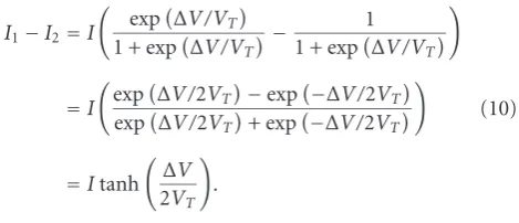
Another very useful operation is obtained by comparing the difference of currents in the differential pair ofFigure 2:
I1−I2=I
expΔV /VT
1 + expΔV /VT
− 1
1 + expΔV /VT
=I
expΔV /2VT
−exp−ΔV /2VT
expΔV /2VT
+ exp−ΔV /2VT
=Itanh
ΔV
2VT
.
(10)
The above operation is indeed very useful, since a pos-terior expectation of a binary random variable (in AWGN channel) is given by a hyperbolic tangent, that is,EX|Y{X} =
tanh((1/σ2
n)y).
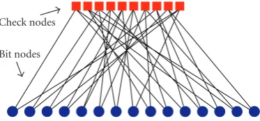
4. ANALOGUE IMPLEMENTATION OF A LOW-DENSITY PARITY-CHECK CHANNEL DECODER
Check nodes
Bit nodes
Figure4: Bipartite graph of the LDPC rate-6/15 code.
be an integral part of a MIMO system. It should be clear that it makes perfect sense to implement both the MIMO and the channel decoder operations in one analogue circuitry. In this section we outline the design of an analogue Low-Density Parity-Check (LDPC) decoder.
The code of choice is a LDPC code of rate 6/15. This is a very short length code for a LDPC code, whose parity-check matrix is not really “low density.” However we will keep re-ferring to it as a LDPC code for the clarity of presentation. LDPC codes are conveniently described by bipartite graphs. A bipartite graph represents pictorially the parity-check ma-trix of a LDPC code. It is also useful in the detection, since the sum-product algorithm operations can be described on
such graph; see, for example, [12]. The bipartite graph of the
chosen 6/15 code is shown inFigure 4. The layout of the
ana-logue decoder for this code is shown inFigure 5. The squares
inFigure 5are the check-node analogue processors and the circles are the bit-node analogue processors. It is basically an unfolded version of the bipartite graph. All operations within the check and bit nodes are performed in the voltage-domain. For further details of implementation of similar bi-nary decoders and a discussion on current/voltage-domain
implementation trade-offs, we refer to an excellent
mono-graph [3].
Figure 6depicts a response of the analogue decoder and outputs of “digitally implemented” sum-product algorithm
with a high level of noise (Eb/N0 = 0 dB) for a given
re-ceived sequence. In this case, the iteration-based (digital) and
the analogue decoder give amazingly similar results.Figure 6
shows actually a close-up of the first microseconds of the analogue response and the first iterations of the digital one to illustrate how the error correction is performed mainly at these first steps of the decoding process. The message sent was 001100, encoded as 111110100001100. However, the re-ceived values would be initially hard decoded as 001010 (i.e., with errors in the bits 4 and 5). Considering the digital de-coder, the two errors are corrected in the first and third it-erations, respectively, while with the analogue decoder they are corrected after a transient of 0.99 and 1.87 microsec-onds. Both responses are incredibly similar, almost as if the
L-values at each iteration of the digital decoder were the
sam-pled points of the contiguous time waveforms of the ana-logue decoder. This, however, is just a mere observation and it is presented here more as a curiosity and not as a re-sult.
5. ANALOGUE IMPLEMENTATION DETAILS OF THE MIMO A POSTERIORI PROBABILITY DECODER
As indicated in (4), the fundamental operations required to
be implemented are multiplication, summation, and nega-tive exponential function, that is, exp(−x). In this section we discuss how those basic blocks can be implemented in ana-logue circuits.
5.1. Multiplier
The most important function that has to be implemented with analogue circuits is multiplication of two input voltages, both of which can be positive or negative. A four-quadrant multiplier circuit is therefore needed to achieve this. This ba-sic block is used most often in the analogue MIMO
detec-tor. The Gilbert multiplier circuit [8] performs
multiplica-tion using the output from a differential pair as the input for
another two differential pairs; seeFigure 7. The circuit is ar-ranged in such a way that the output current is given by the combination of all four upper currents:
I13+I24
−I14+I23
=Ibtanhk
V1−V2
2 tanh
kV3−V4
2 .
(11)
The output current and voltage of the Gilbert multiplier
fol-low a tanh(x) rule, which for small input voltage differences
can be approximated by tanh(x)≈ x. Additionally, this
ba-sic circuit has a limitation on the inputs: max(V3,V4) >
min(V1,V2).
Multiplication is typically performed on random
volt-ages. Hence, it is difficult to make any assumptions about
the range of the input signals. A wide-range multiplier [8]
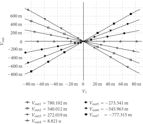
is required in order to ensure that the circuit works prop-erly for both high and low input voltage levels. One possible choice is the wide-range Gilbert multiplier circuit, shown in
Figure 8. The wide-range multiplier isolates the bottom
dif-ferential pair from the upper differential pairs using current
mirrors. This allows the range ofV3andV4to be
indepen-dent ofV1andV2allowing the circuit to work properly for
input voltages close to the supply voltage. The SPICE simu-lated output of the wide-range Gilbert multiplier is shown in
Figure 9. The figure showsVout as a function ofV1, for
dif-ferent choices ofV2. The observed voltage is closely
approxi-mated byΔVout =V1V2/Vref (withVref =10 mV). For high
input values the tanh(x) behaviour starts being noticed,
de-grading the output characteristic of the circuit. For moderate input values, up to 30–60 mV, the linearity is high enough to multiply the two inputs with great accuracy.
5.2. Summation
The summation operation is most conveniently performed
Check
Check
Check
Check Bit
Bit
Bit Check
Bit
Bit
Bit
Check
Check
Check Bit
Bit
Bit Check
Bit
Bit
Bit
Check Bit
Bit
Bit
Figure5: Layout of the analogue LDPC code decoder.
150
100
50
0
−50
−100
−150
Log-MPP
ratio
(mV
)
0 1 2 3 4 5 6 7 8 9 10
Iteration Bit 10
Bit 11 Bit 12
Bit 13 Bit 14 Bit 15 (a)
100 mV
50 mV
0 mV
−50 mV
−100 mV
0 2 4 6 8 10
Time (μs) (b)
Vdd Vdd Vdd Vdd
I13 I14 I24 I23
V3
V4
V3
I1 I2
V1 V2
Ib
Vb
Figure7: Gilbert multiplier basic cell.
Vdd Vdd Vdd Vdd Vdd Vdd
M19 M4
M1 M18 M2 M3
M5 M6 V21i M7 M8 Vout 1
V22i
V22i
m11 m12 m13 m14 m16 m17
V11i V12i
m15
Vb
Vss Vss Vss Vss Vss
Figure8: Wide-range Gilbert multiplier.
enough just to connect the wires in a node. Indeed, such summers are used in the MIMO decoder in the “margina-liser” block. A voltage summation is also required to avoid excessive number of voltage-current-voltage
transforma-tions. A circuit [13] capable of performing voltage
summa-tion is shown inFigure 10. By simple analysis of the circuit,
the output voltage can be obtained as a function of the gate-source voltages of the transistors [13]:
ΔVOS=
(W/L)1 (W/L)2
VGS1−VGS2
+VGS3−VGS4
=
(W/L)1 (W/L)2
ΔV1+ΔV2
,
ΔVOS=VO1−VO2, ΔV1=V11−V12,
ΔV2=V21−V22,
(12)
where W and L are the width and length of a transistor
respectively. Figure 11 shows the simulated response for
(W/L)1=(W/L)2(W=16μandL=1.6μ).
5.3. Negative exponential
The last building block needed to implement the analogue MIMO detector is a circuit with a negative exponential response in the voltage domain, that is,
ΔVout=KVrefexp
−ΔVin
Vref
, (13)
whereVrefis a reference voltage,ΔVinandΔVoutare the input
and output differential voltages, respectively, andKis a
nor-malisation constant that has no effect on the response of the
600 m 400 m 200 m 0
−200 m
−400 m
−600 m
−800 m Vout
−80 m−60 m−40 m −20 m 0 20 m 40 m 60 m 80 m
V1
Vout1=780.102 m
Vout2=540.012 m
Vout3=272.019 m
Vout4=8.821 u
Vout5= −273.341 m
Vout6= −545.963 m
Vout7 = −777.315 m
Figure 9: Output characteristics of the wide-range Gilbert
mul-tiplier. The plots correspond to the second input set at±90 mV, ±60 mV,±30 mV, and 0 V.
low as possible we use a simple approximation for the nega-tive exponential function. A simplified equation for the drain current through a saturated nMOS transistor in the strong inversion region is
ID=K
2
W L
VGS−VT 2
, (14)
where K is a technology-dependent factor, W and L are
width and length of the transistor, VGS is the gate-source
voltage applied, andVTis the threshold voltage. We can
ap-proximate the negative exponential by a function of the type
f(x)=A−B√xusing a single transistor fed with a currentId
that we obtain from a transconductance stage. For small in-put values such approximation is good enough for our pur-poses. However, if the input grows bigger, the approximation function can become negative where the true exponential would not. Therefore, it is required to clip the output voltage to ensure it never becomes negative. The final circuit is
de-picted inFigure 12. Transistors M9—M17 form a
transcon-ductance amplifier [8] that converts the input voltage into a
current. This current is passed to a transistor M1 that per-forms the approximation function. Transistors M2 and M3 restrict the output to positive values, and finally, M4–M8 are used to shift the output voltage to an adequate level for inter-connection with other building blocks.
Figure 13depicts simulation results of this circuit. The
ideal response shown corresponds to (13) withK =1.8 and
Vref =10 mV. The thick line is the error between the ideal
response and the approximation.
The one remaining operation|x|2is simply achieved by
a four-quadrant multiplier realisingx·x.
M7
M3
V12
V11
V22
V21
Vdd
M8
M4
M5 M6
VO1 VO2
M1 M2
m9 m10
Vg Vg
Vss Vss
Figure10: Voltage differential adder circuit.
×102 8 m 6 m 4 m 2 m 0
−2 m
−4 m
−6 m
−8 m Vout
−4 m −3 m −2 m −1 m 0 1 m 2 m 3 m 4 m
×102
V1
AV1= −531.342 m
AV2= −327.256 m
AV3= −120.073 m
AV4=86.990 m
AV5 =290.907 m
Figure11: Output characteristics of the differential adder circuit.
The plots correspond to the second input set at±400 mV,±200 mV and 0 V.
6. ANALOGUE MIMO DECODER EXAMPLE AND RESULTS
We have simulated in the SPICE software an analogue MIMO decoder with 3 transmit and 3 receive antennas. All transis-tor models used here are basic models (standard BSIM 3v3 MOS model) supplied with nearly all SPICE software pack-ages. A BPSK modulation was assumed. Six bits of data are
encoded to 15 (coded) bits by the LDPC code ofSection 4.
The MIMO decoder consists of 5 identical modules, each providing MPPs for 3 coded bits. The outputs of the MIMO decoder are wired directly to the analogue LDPC decoder.
One of the modules is presented in Figure 14. The layout
of the module corresponds to a factor graph that describes
Vdd Vdd Vdd Vdd
M14 M15
M12
Vin 2
Vin 1
M9 M10
Vb
M16 M17
M13
M11
M19 M20
M18 M21
Vd1 Vd2 Vdd Vdd
M4 M5
M7
M1 M2
M8 M3
VO1
VO2
M6
Vb
Vref
Figure12: Block diagram of the negative exponential MOS circuit.
15 m
10 m
5 m
0 m Vout
0 20 m 40 m 60 m 80 m 100 m
V
Figure13: Output characteristic obtained from SPICE and the ideal response.
blocks performs analogue computations corresponding to (4).
The outputs of the modules are fed to the marginaliser block. The marginaliser consists of triple output cascode current mirrors and appropriately connected wires to
ob-tain current summations.Table 1 depicts results of a
com-parison between the analogue LDPC decoder and a stan-dard sum-product detection (software simulation of a
dig-ital decoder). An error is defined as a difference in
poste-rior probability estimates of a given bit being zero, that is,
Error = PrAPP (b = 0)−PrAnalogue (b = 0). A great
accu-racy of the analogue decoder can be observed.Table 2depicts
comparison results between the analogue MIMO decoder and a simulated exact a prosteriori probability (APP) MIMO decoder (full enumeration without any approximations). A good accuracy of analogue MIMO decoder can be observed, albeit inferior to that of the LDPC decoder. The inaccuracies are introduced mainly by the approximation in the exponen-tial function and variations in the currents due to the non-ideal behaviour of the transistors.
7. CONCLUSIONS
In this contribution we have proposed an analogue detector
for a MIMO system. It is expected that such decoder will offer
similar advantages to those reported by analogue binary de-coders, that is, significant improvements in processing speed,
reduction in transistor count, power efficiency, and heat
dis-sipation. On the downside, since the decoder mimics the full
complexity APP decoder (albeit very efficiently), the
transis-tor count (not the processing speed) increases exponentially. Such MIMO decoder may still be feasible for a MIMO system with small number of transmit antennas and simple modu-lation formats. However, one of the major challenges seems to be the design of reduced-complexity high-performance al-gorithms that could be executed in analogue VLSI networks.
It is very difficult to envisage modern receivers
com-pletely deprived of DSP/FPGAs. Wireless receivers per-form many other logical operations (apart from the
de-tection) that can efficiently be executed only in software
V1 1.005 ±
±
Rii1Rii2Ri j1Ri j2
V2 0.995
σ2inv 1 σ2inv 2 Rx3 1
Rx3 2 Rx 1 Rx 2
VO11
VO12
In 1 In 2
VO21
VO22
var(−1)1 var(−1)2 R33 1R33 2
V100
1
V3 ±
R22 1R22 2R23 1R23 2
Rx2 1
Rx2 2
Rii1Rii2Ri j1Ri j2
Rx 1 Rx 2 In 1 In 2
VO11
VO12
VO21
VO22
var(−1)1 var(−1)2
σ2inv 1 σ2inv 2
R12 1 R12 2 VV1112
R13 1 R13 2 V21 V22 Vout1 Vout2
RPP1
RPP2
R12 1 R12 2
V11
V12
R13 2 R13 1 VV2122
Vout1
Vout2
RPn1
RPn2
R22 1R22 2R23 2R23 1
Rx2 1 Rx2 2
Rii1Rii2Ri j1Ri j2 Rx 1
Rx 2 In 1 In 2
VO11
VO12
VO21
VO22
var(−1)1 var(−1)2
σ2inv 1 σ2inv 2
R11 1R11 2Rpp1Rpp2
Rx1 1
Rx1 2
Rii1Rii2Ri j1Ri j2 Rx 1
Rx 2
In 1 In 2
VO11
VO12
VO21
VO22
var(−1)1 var(−1)2
σ2inv 1σ2inv 2
R11 1R11 2Rpn2Rpn1
Rx1 1
Rx1 2
Rii1Rii2Ri j1Ri j2 Rx 1
Rx 2
In 1 In 2
VO11
VO12
VO21
VO22
var(−1)1 var(−1)2
σ2inv 1σ2inv 2
R11 1R11 2Rpn1Rpn2
Rx1 1
Rx1 2
Rii1Rii2Ri j1Ri j2 Rx 1
Rx 2
In 1 In 2
VO11
VO12
VO21
VO22
var(−1)1 var(−1)2
σ2inv 1σ2inv 2
R11 1R11 2Rpp2Rpp1
Rx1 1
Rx1 2
Rii1Rii2Ri j1Ri j2 Rx 1
Rx 2
In 1 In 2
VO11
VO12
VO21
VO22
var(−1)1 var(−1)2
σ2inv 1σ2inv 2
Transcond. V1 V2 Iout1 Iout2 Iout3
I11 I12 I13 Transcond. V1 V2 Iout1 Iout2 Iout3
I21
I22 I23
Transcond. V1 V2 Iout1 Iout2 Iout3
I31 I32 I33
Transcond. V1 V2 Iout1 Iout2 Iout3
I41 I42 I43
Transcond. V1 V2 Iout1 Iout2 Iout3
I51 I52
I53
Transcond. V1 V2 Iout1 Iout2 Iout3
I61
I62 I63
Transcond. V1 V2 Iout1 Iout2 Iout3
I71 I72
I73 Transcond. V1 V2 Iout1 Iout2 Iout3
I81
I82
I83
Figure14: Layout of the basic module of the analogue APP MIMO decoder.
Table1: Analogue LDPC decoder comparison results.
Eb/N0(dB) Mean (absolute value (error)) Variance (error)
0 2.90e−03 5.92e−05
1 5.00e−03 1.86e−04
2 4.90e−04 1.24e−05
3 1.08e−08 2.36e−15
5 2.91e−09 1.62e−16
7 4.37e−10 1.07e−17
would be a mixed-mode architecture, where the analogue
decoder would act as a highly specialised and very efficient
“subcontractor,” that is, a coprocessor working together with
Table2: Analogue MIMO decoder comparison results.
Eb/N0(dB) Mean (absolute value (error)) Variance (error)
0 0.020 60 0.000 86
1 0.026 50 0.001 50
2 0.020 90 0.001 10
3 0.018 20 0.000 95
5 0.014 20 0.000 73
7 0.012 70 0.000 93
9 0.013 00 0.001 30
ACKNOWLEDGMENT
R. Piechocki and J. Garrido would like to thank Toshiba TRL Ltd for sponsoring their research activities.
REFERENCES
[1] H.-A. Loeliger, F. Lustenberger, M. Helfenstein, and F. Tarkoy, “Probability propagation and decoding in analog VLSI,” in
Proceedings of IEEE International Symposium on Information Theory (ISIT ’98), pp. 146–146, Cambridge, Mass, USA, Au-gust 1998.
[2] J. Hagenauer and M. Winklhofer, “The analog decoder,” in
Proceedings of IEEE International Symposium on Information Theory (ISIT ’98), pp. 145–145, Cambridge, Mass, USA, Au-gust 1998.
[3] F. Lustenberger,On the design of analog iterative VLSI decoders,
vol. 2 ofSeries in Signal and Information Processing, Hartung-Gorre, Konstanz, Germany, 2000, Ph.D. dissertation. [4] A. Xotta, D. Vogrig, A. Gerosa, et al., “An all-analog CMOS
implementation of a turbo decoder for hard-disk drive read channels,” inProceedings of IEEE International Symposium on Circuits and Systems (ISCAS ’02), vol. 5, pp. 69–72, Scottsdale, Ariz, USA, May 2002.
[5] A. F. Mondragon-Torres, E. Sanchez-Sinencio, and K. R. Narayanan, “Floating-gate analog implementation of the ad-ditive soft-input soft-output decoding algorithm,”IEEE Trans-actions on Circuits and Systems—Part I: Fundamental Theory and Applications, vol. 50, no. 10, pp. 1256–1269, 2003. [6] V. C. Gaudet and P. G. Gulak, “A 13.3-Mb/s 0.35-μm CMOS
analog turbo decoder IC with a configurable interleaver,”IEEE Journal of Solid-State Circuits, vol. 38, no. 11, pp. 2010–2015, 2003.
[7] C. Winstead, J. Dai, S. Yu, C. Myers, R. R. Harrison, and C. Schlegel, “CMOS analog MAP decoder for (8,4) Hamming code,”IEEE Journal of Solid-State Circuits, vol. 39, no. 1, pp. 122–131, 2004.
[8] C. Mead,Analog VLSI and Neural Systems, Addison-Wesley, Reading, Mass, USA, 1989.
[9] R. Herken, Ed.,The Universal Turing Machine: A Half-Century Survey, Oxford University Press, Oxford, UK, 1988.
[10] J. Hagenauer, E. Offer, C. Measson, and M. Moerz, “Decod-ing and equalization with analog non-linear networks,” Eu-ropean Transactions on Telecommunications, vol. 10, pp. 659– 680, 1999.
[11] A. Paulraj, R. Nabar, and D. Gore,Introduction to Space-Time Wireless Communications, Cambridge University Press, Cam-bridge, UK, 2003.
[12] S. Haykin, Communication Systems, John Wiley & Sons, Chichester, West Sussex, UK, 4th edition, 2001.
[13] J. S. Pena-Finol and J. A. Connelly, “A MOS four-quadrant analog multiplier using the quarter-square technique,”IEEE Journal of Solid-State Circuits, vol. 22, no. 6, pp. 1064–1073, 1987.
Robert J. Piechocki received his M.S. degree from the Technical University of Wroclaw, Poland, in 1997 and his Ph.D. degree from the University of Bristol in 2002, both in electrical engineering. He is currently a Research Fellow at the Centre for Communications Research, University of Bristol. His research interests lie in the areas of statistical signal processing for communications and radio channel modelling for wireless systems.
Jose Soler-Garridoreceived the Telecom-munications Engineer degree from the Polytechnic University of Valencia, Spain, in 2004. Currently he is pursuing his Ph.D. degree in the Department of Electrical and Electronic Engineering, University of Bristol, UK. His main research interests include analogue VLSI design for detec-tion/decoding and MIMO wireless systems.
Darren McNamara received the M. Eng. degree in electrical and electronic engineer-ing from the University of Bristol, UK, in 1999. During this period he was spon-sored by Racal Radio Ltd, where he fol-lowed their graduate training programme and worked on wireless communication systems. In 2003 he received the Ph.D. de-gree, also from the University of Bristol, in the area of MIMO channel measurement
and analysis. Since November 2002 he has been with the Toshiba Telecommunications Research Laboratory in Bristol, UK.
Joe McGeehan received the B. Eng. and Ph.D. degrees in electrical and electronic engineering from the University of Liver-pool, UK, in 1967 and 1971, respectively. He is presently a Professor of communications engineering and Director of the Centre for Communications Research at the University of Bristol. He is concurrently the Managing Director of Toshiba Research Europe Lim-ited: Telecommunications Research