Adiabatic Logic Circuit Design
Vibhu Bindal
( Electronics & Communication Engineering, MIT Moradabad, U.P., India - 244001 ) [email protected]
ABSTRACT
The word ADIABATIC is derived from the Greek word ADIABATOS which means there is no exchange of energy with the environment and hence no energy loss in form of heat dissipation. Adiabatic logic is the term given to low power electronics circuits that implement reversible logic. Adiabatic logic is commonly used to reduce the energy loss during the charging and discharging process of circuit operations. Adiabatic logic is also known as energy recovery or charge recovery logic. The adiabatic logic structure dramatically reduces power dissipation. The adiabatic switching technique can achieve very low power dissipation but at the expense of complexity.
Keywords –CMOS, SCRL, ECRL, AL.
I.
INTRODUCTION
The adiabatic logic reduces power dissipation. The term adiabatic comes from the thermodynamics used to describe a process in which there is no exchange of heat with the environment. These types of circuits are low power circuits which use reversible logic to conserve energy. The term comes from the fact that an adiabatic process is one in which the total heat or energy in the system remains constant. In this technique instead of discharging the consumed energy is recycled back to the power supply thereby reducing overall power consumption. Adiabatic logic offers a way to use the energy stored in the load capacitors rather than the traditional way discharging load capacitor to the ground and wasting this energy. Adiabatic logic can be achieved by ensuring that the potential across the switching devices is kept small. This can be achieved by charging the capacitor from a time-varying voltage source or constant current source.
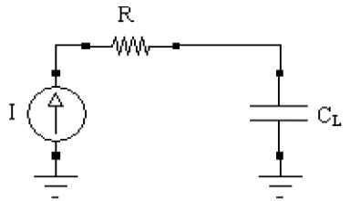
Fig. 1: Schematic for adiabatic charging process
Here R represents the resistance of the PMOS
network. A constant charging current
corresponds to a linear voltage ramp. Assuming
that the capacitance voltage VRc Ris 0 initially. The
variation of the voltage as a function of time can
be found as VRcR(t) = IRsR . t/2
Then, Charging current IRs R= C . VRcR(t) / 2
The amount of energy dissipated in the resistance R from t = 0 to T can be found as
ERdissR = R ʃ T IRsRP
2
P
dt
= R . IRsRP
2
P
. T
The dissipated energy during this charge up transition can also be expressed as
ERdiss R= (RC/T) . C . VRcRP 2
P
(t)
From this equation we can say that the dissipated energy is smaller than for the conventional case if the charging time T>>2RC and can be made small by increasing the charging time. A portion of the energy thus stored in the capacitance can also be reclaimed by reversing the current source direction, allowing the charge to be transferred from the capacitance back into the logic. Adiabatic logic circuits thus require non-standard power supplies with time-varying voltages also called pulsed power supplies. Adiabatic Circuits reduce dissipation by following key rules:
• Never turn on a transistor when there is a voltage potential between source & drain.
• Never turn off a transistor when current
is flowing through it.
II.
CONCEPT OF LOW POWER
Low power is needed because of desirability of portable devices like cell phone batteries and in biomedical field like in heart pacemakers, however large power dissipation requires larger heat sinks hence increased area. So the main purpose is to provide new low power solutions for VLSI designers. There are two types of power dissipation:
• Dynamic Component
• Static Component
Dynamic Component consists the signal transitions and short-circuit power dissipation while static component consists leakage power dissipation.
PRavgR = PRswitchingR + PRshort-cktR + PRleakage
= αR0‒›1R CRL RVRDDRP
2
P
fRclkR + IRscR VRDDR + IRleakageR VRDD
where CRLR = Loading capacitance
fRclkR = Clock frequency
α = Switching activity
To reduce the power consumption, reduce the dynamic power component which is the first term in the equation of power. When the dynamic power is reduced then the total power consumption is reduced. The term of dynamic
power in power equation is αR0‒›1R CRL RVRDDRP
2
P
fRclkR .
The dynamic power directly depends upon the
supply voltage VRDDR. If we reduce the supply
voltage VRDDR, then the dynamic power reduced.
Except this decrease physical capacitance, reduce glitches and reduction in rise or fall time also results a decrease in dynamic power. There are following limitations in reduction of power:
1. Reduction in VRDDR without
correspondingly reducing VRtR reduces
speed then VRDDR must be at least 2VRtR.
2. Issue of compatibility.
3. Reductions in physical capacitance by
reducing size of devices reduce driving capability and hence speed.
III.
ADIABATIC LOGIC FAMILIES
Most research has focused on building
adiabatic logic out of CMOS. However,
current CMOS technology, though fairly
energy efficient compared to similar
technologies, dissipate energy as heat,
mostly when switching. Several designs of
adiabatic CMOS circuits have been
developed. Adiabatic logic circuits are also
use current nanomaterials such as silicon
nanowires or carbon nanotubes since
nanoelectronics are expected to dissipate a
great amount of heat. There are 2 types of
adiabatic logic families:
•
Fully adiabatic logic family.
•
Quasi adiabatic logic family.
Fully adiabatic logic family circuits lose
their energy due to leakage currents through
non-ideal switches. Quasi adiabatic logic
family circuits suffer from the non-adiabatic
energy loss in some regions of operations
that is usually proportional to the
capacitance driven and the square of the
threshold voltage. There are following
classified families of adiabatic logic:
•
Split level Charge Recovery Logic.
•
Two level Adiabatic Logic.
•
Positive Feedback Adiabatic Logic.
•
Efficient Charge Recovery Logic.
•
Two Phase clocked adiabatic static
CMOS logic.
IV.
SPLIT LEVEL CHARGE
RECOVERY LOGIC
Knight and Younis developed a family of adiabatic circuits known as split level charge recovery logic. Analysing a full cycle of the SCRL NAND represented in figure.
R
Fig. 2: SCRL adiabatic circuit
The circuit is similar to a conventional NAND; however, one of the main differences is that the top and bottom rails are driven by trapezoidal
clocks (Φ1and /Φ1) rather than VRDDR and ground.
Initially the whole circuit is set at VRDDR/2 except
for P1 which is set to ground and /P1 is set to
VRDDR so that the transmission gate is OFF. In the
next step, the transmission gate is turned ON by gradually switching the value of P1 and /P1.
Following Φ1and /Φ1which were at VRDDR and
ground respectively. At this point, the gate computes the NAND of A & B like a non-adiabatic gate would. Once the output is used by the next gate, the transmission gate can be turned back OFF gradually. Then Φ1and /Φ1 are
gradually returned to VRDDR/2 and now the input
can change and the next cycle can begin. It is important not to change the input until the rails
are back to VRDDR/2 so that a transistor is not
turned ON when there is a potential difference. The last part that needs explaining is the extra PMOS connected to input B. Lets analyse what happens when that transistor is missing. Once Φ1and /Φ1 are split, When A has a value of logical 1 and B of logical 0, current flows from
VRDDR through the PMOS controlled by B and
down through the NMOS controlled by A which means that a high voltage is passing through an NMOS which will thus dissipate energy. This problem is solved by the extra PMOS and in general case must be taken to ensure that an internal node is not dissipating energy in this way. Finally the only node that is not restored by the gate is the output. This is so that a fully pipelined circuit at the gate level can be achieved. Also, in order to achieve the gradual swings needed to operate these gates, trapezoidal
clock are used so that initially, the voltage is held constant for quarter of a cycle then gradually gets turned up or down, held constant again and for the final quarter is gradually
returned to the initial value
.
V.
TWO LEVEL ADIABATIC
LOGIC
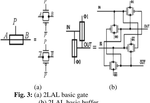
Another interesting adiabatic logic family is the two level adiabatic logic (2LAL) developed by Frank. Like SCRL, this family can be fully pipelined at the gate level. Figure shows the basic building block of 2LAL, a pair of transmission signal A and /A respectively.
(a) (b)
Fig. 3: (a) 2LAL basic gate (b) 2LAL basic buffer
Figure 3(b) shows the basic buffer element of 2LAL which consists of two sets of transmission gates. Φ1and Φ0 are both trapezoidal clocks but Φ1is a quarter behind Φ0. Initially all the nodes are at 0. As the input gradually raises to 1, Φ0
transitions to 1. On the next step, Φ1transitions
to 1. Which sets the output to 1 if the input was one and otherwise leaves it at 0 which in itself reduces the power dissipation because no charge passes through the transistor. On the third step, Φ0 transitions back to 0 resting the input to 0. Finally Φ1transitions back to 0 and the output is restored to 0 by the following gate in order to accommodate for full pipelining and thus the circuit is ready to process a new input. Another feature of 2LAL is that inverters can be easily created by simply crossing over the rails when going from one gate to the next.
VI.
POSITIVE FEEDBACK
ADIABATIC LOGIC
The structure of PFAL is shown in figure 4. Two n-trees realise the logic functions. This logic family also generates both positive and negative outputs. The major difference with respect to ECRL that the latch is made by 2 PMOS and 2 NMOS rather than by only 2 PMOS as in ECRL and that the functional blocks are in parallel with the transmission PMOS. Thus the equivalent R is smaller when the capacitance needs to be charged. The ratio between the energy needed in a cycle and the dissipated one can be seen in figure 3.4.
Fig. 4: PFAL logic circuit
During the recovery phase, the loaded capacitance gives back energy to the power supply and the supplied energy decreases. The partial energy recovery circuit structure so called Positive Feedback Adiabatic Logic.
VII.
EFFICIENT CHARGE
RECOVER LOGIC
ECRL consists of 2 cross coupled PMOS transistors in the pull up section whereas the pull down section is constructed with a tree of NMOS transistors. Its structure is similar to the cascade voltage switch logic with differential signalling. The logic function in the functional block can be realized with only NMOS transistors in pull down section.
VIII.
TWO PHASE CLOCKED
ADIABATIC STATIC CMOS
LOGIC
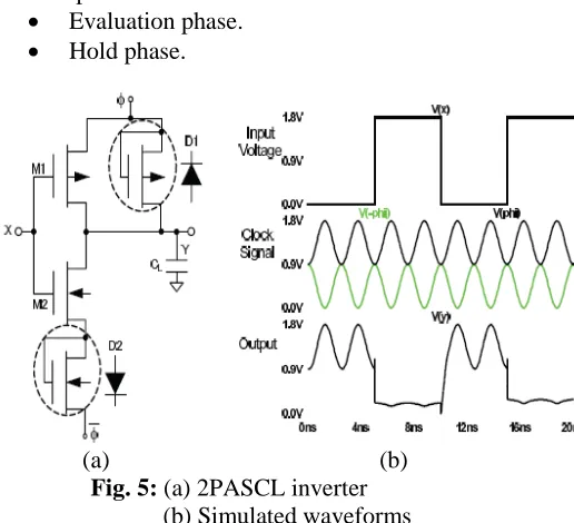
Figure 5 (a) and (b) shows a circuit diagram and waveforms illustrating the operation of the 2PASCL inverter. It resembles the static CMOS logic inverter but operates in a nearly adiabatic fashion. The first difference between 2PASCL and static CMOS logic gate is the two diodes, one from the output node to the power clock supply and another one is placed next to the NMOS logic to another power clock. Both MOS diodes are used to recycle the charges from the output node to improve discharging speed of internal signal nodes with a long chain of switches before them. The other difference is that split-level sinusoidal power clock supplies.
Φ and /Φ are used to replace the VRDDR and VRSSR.
Substrate of PMOS is connected to the Φ whereas for NMOS, it is connected to the /Φ. From the simulation we found that split-level sinusoidal gives a lower energy dissipation compared to trapezoidal waveforms to maximum values. By using two split-level sinusoidal waveforms where each peak to peak is 0.9V, we can reduce the voltage difference thus reducing the charging and discharging activities. The circuit operation phase is divided into two phase:
• Evaluation phase.
• Hold phase.
(a) (b)
Fig. 5: (a) 2PASCL inverter (b) Simulated waveforms Evaluation phase is when the voltage driver Φ swings up and /Φ swings down. The opposite, hold is when /Φ swings up and Φ swings down. In evaluation phase, when the output node Y is low and PMOS transistor resulting in the high state at the output. When Y is low and NMOS is
on, no transition occurs. The same result is gained when the output node is high and PMOS is on. Finally when Y node is high and NMOS is on, discharging via NMOS and D2 resulting in
the decrease of output voltage to VRtR value where
the logical state is 0. At hold phase, due to the diodes, the state of Y when preliminary state is low remains unchanged. When the preliminary state of the output node is high, it will change to
VRtR, the threshold voltage of the diode. At this
point, discharging via diode D1 occurs. From the operation of 2PASCL as explained in evaluation and hold phase, less dynamic switchings are observed as circuit nodes are not necessarily charging and discharging every clock cycle which reduces the node switching activities significantly.
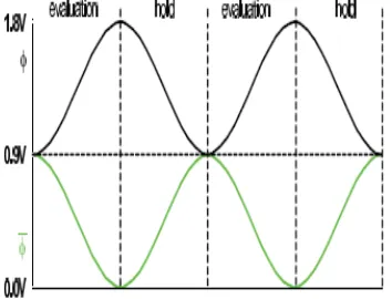
Fig. 6: Clocked voltage driver showing the evaluation and hold phase
IX. COMPARISON OF CHARGING
PROCESS OF ADIABATIC LOGIC TO STATIC CMOS
A simple CMOS inverter is shown in figure. The capacitor C at the output of gate represents the
output capacitance of following gates.
Depending on the input signal, in steady state either the PMOS device or the NMOS device is on, the remainder is off. If the input transition from 1 to 0 occurs, energy is transferred from the voltage source to charge the output capacitor
to the voltage VRDDR. A charge of Q = C.VRDDR is
taken from the voltage source, an energy
quantum of ERvR = Q.VRDDR = C.VRDDRP
2
P
is withdrawn from the voltage source. The energy stored on
the capacitor at the voltage VRDDR is equals to
ERcR = (1/2).C.VRDDRP
2
The difference between the delivered energy and the stored energy is dissipated in the PMOS switch. Now, if the input switches from 0 to 1, in steady state condition the NMOS channel is ON, the PMOS OFF. Charge stored on the output capacitance is then dissipated via the NMOS device to ground. The energy dissipation of a switching event in a static CMOS is given as
ERCMOSR= α. (1/2).C.VRDDRP
2
Where α is the switching probability. As there is no dissipation in static CMOS gates, if there is no switching event at all. Different approaches are useful to reduce the energy dissipation in
static CMOS.
Fig 4.1: Static CMOS inverter
Adiabatic logic doesn’t abruptly switches from 0
to VRDDR, but a voltage ramp is used to charge and
recover the energy from the output. The gate consists of two cross coupled PMOS devices that are used to store the information. The logic function is constructed via two NMOS devices. Cascaded gates are operated by a four phase power clock signal. Input signal for the ECRL
gate are shifted by 90P
o
P
with respect to the applied power clock signal.
Fig. 7: ECRL buffer
To calculate the energy consumed by charging a capacitance adiabatically, the equivalent circuit in figure for an adiabatic gate is used.
Fig. 8: Equivalent circuit for adiabatically loading a capacitance
R is the resistance in the charging path of the circuit, consisting of the on-resistance of transistors in the charging path and the sheet resistance of the signal line. Assume R is to be
constant. The voltage is ramped from 0 to VRDDR
within T, slow enough that VRcR(t) is able to
follow signal V(t) instantly, so VRcR(t) is
approximately equals to V(t). therefore, the current into the circuit can be determined by
The energy for a charging event is calculated by integrating the power P(t) during the transition time T then,
The integral of VRcR(t).i(t) over one clock cycle
will be 0, as no energy is dissipated in the
capacitance. Thus by replacing VRRR(t) with i(t).R
results in
A whole cycle consists of charging and recovering. As the recover process will lead to the same amount of energy dissipation, the overall dissipation in adiabatic logic (AL) is
The following equation shows the operating speed impacts the energy dissipation. The slower the circuit is charged, the less energy is dissipated. The opportunity to further reduce the consumption by scaling the supply voltage or by reduction of the capacitive load also exists in adiabatic logic.
X. SIMULATION
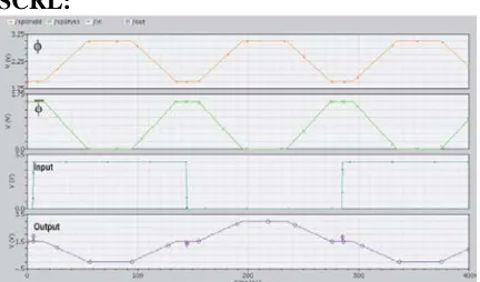
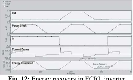
Simulated waveforms of inverters and their energy recover waveforms are following:
SCRL:
Fig. 9: Simulated waveform of SCRL Inverter
Fig. 10: Energy recovery in SCRL inverter
ECRL:
Fig. 11: Simulated waveform of ECRL inverter
Fig. 12: Energy recovery in ECRL inverter
XI. RESULT
The simulated waveforms of SCRL and ECRL inverters are shown in graph. Also their energy recovery graphs are shown in figure.
XII. CONCLUSION
The comparison of the adiabatic logic methodologies with CMOS circuit has proved that power consumption with the proposed logic is for less as compared to CMOS. For instance, when the input frequency varies from 10 to 150MHz, the proposed inverter and 1-bit full adder circuits dissipate minimally as only 12% and 21% power of the total power of a static CMOS based logic circuit. These advantages made this logic more convenient for energy efficient digital applications. A comparison of power dissipation between CMOS and adiabatic logic is shown by the histogram.
Fig. 13: Histogram showing the power dissipation
REFERENCES
1] Anamika Mishra, Anju Jaiswal, Ankita Jaiswal, A.K.Niketa, “Design and Analysis
of Conventional CMOS and Energy
Efficient Adiabatic Logic for Low Power VLSI Application,” International Journal of Engineering and Advanced Technology (IJEAT), Volume-3, Issue-12, May 2014.
[2] B. Dilli Kumar and M. Bharathi, “Design of Energy Efficient Arithmetic Circuits Using Charge Recovery Adiabatic Logic,” International Journal of Engineering Trends and Technology- Volume4, Issue1 – 2013.
[3] N. Anuar, Y. Takahashi and T. Sekine, “Two phase clocked adiabatic static logic circuit: a proposal for digital low power applications,” Proc.IEICE Gen. Conf., p.102, Mar. 2009.
[4] Y. Takahashi, T. Sekine, and M.Yokoyama, Theoretical analysis of power clock generator based on the switched capacitor regulator for adiabatic CMOS logic, Proc. IEEE Conf. Argentine School of Micro-Nanoelectronics, Technology and Applications, Argentine, Sept. 18-19, 2008.
[5] M.S.Dhaka, Gayatri and P.Singh Dhaka, “Adiabatic Logic Gate for Low Power Application,” International Journal of Engineering Research and Applications, Vol. 2, No. 3, pp. 2474-2478, 2012.