ISSN (Print) : 2320 – 3765 ISSN (Online): 2278 – 8875
I
nternational
J
ournal of
A
dvanced
R
esearch in
E
lectrical,
E
lectronics and
I
nstrumentation
E
ngineering
(A High Impact Factor, Monthly, Peer Reviewed Journal)
Website: www.ijareeie.com
Vol. 6, Issue 10, October 2017
Designing of Circular Monopole Patch
Antenna Loaded with Split Ring
Resonator
Apoorva D*
Department of Electronics & Communication Engineering, Meerut Institute of Engineering & Technology, Meerut, India
ABSTRACT:The EM conduct of the coplanar waveguide fed, filled split ring resonator to the ultra-wideband antenna
with single band notch symptoms have offered. The proposed size of antenna 30 × 35 × 1.6 mm3 is very compact and
easy to integrate with handheld devices. Here the antenna loaded with SRRs to create single frequency notch in 6.41GHz to 8.26 GHz used for X-band satellite communication. The radiation pattern of H-plane is omnidirectional and radiation pattern of E-plane exhibits like a dipole. The antenna gain is stable across the absolute operating frequency besides at notch. Therefore, a VSWR <2 with a large bandwidth was clearly identifiable. This work investigates several
problems simulated using High frequency structure simulatortool.
KEYWORDS: Ultrawideband; Circular monopole; Splitring resonator; Coplanar waveguide; Circular monopole antenna; Effective isotropic radiated power
I. INTRODUCTION
In 2002, the FCC (Federal Communications Commission) release of 10 dB unlicensed bandwidth of 7.5 GHz, ranging from 3.1 to 10.6 GHz by effective isotropic radiated power (EIRP) spectral density as -41.3 dBm/MHz for commercial use in radio communication. The UWB (Ultra Wideband) communication has witnessed all over the world to make use of this bandwidth for enhanced data rate and a variety of other purposes. The UWB communication has the inherent advantage of low power consumption, simple structure,small size and ease of concord together with high transmission rates and relatively good omnidirectional property.While 7.5 GHz bandwidth is the core motivation for developing high data rate devices, which may potentially meddle with UWB communication such as X-band satellite communication system at 8.23GHz. While having wave frequency from 6.19GHz to 8.03 GHz for downlink and 8.03GHz to 8.57 GHz for uplink communication. The antenna being an essential component of UWB communication, it is thus incumbent to design the same having band notched function to avoid interference with the excluding wireless network technologies. The main challenge in designing an UWB antenna for indoor communication system is the avoidance of interference with egress narrowband services, which may cause potential interference.
ISSN (Print) : 2320 – 3765 ISSN (Online): 2278 – 8875
I
nternational
J
ournal of
A
dvanced
R
esearch in
E
lectrical,
E
lectronics and
I
nstrumentation
E
ngineering
(A High Impact Factor, Monthly, Peer Reviewed Journal)
Website: www.ijareeie.com
Vol. 6, Issue 10, October 2017
II. PROPOSED ANTENNA DESIGN
A Coplanar Waveguide feed circular monopole antenna with return loss graph, which shows below -10dB for entire UWB bandwidth 3.1GHz to 10.6 GHz in Figure 1.
Figure 1:Circular monopole antenna CMA.
Figure 2: Simulated graph of CMA.
ISSN (Print) : 2320 – 3765 ISSN (Online): 2278 – 8875
I
nternational
J
ournal of
A
dvanced
R
esearch in
E
lectrical,
E
lectronics and
I
nstrumentation
E
ngineering
(A High Impact Factor, Monthly, Peer Reviewed Journal)
Website: www.ijareeie.com
Vol. 6, Issue 10, October 2017
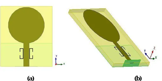
(a) (b)
Figure 3: Design of proposed antenna (a) top view and (b) side view of antenna.
The proposed antenna has optimized by using HFSS (High Frequency Structure Simulator). The rectangular shaped SRR is placed on the side by side of the CPW feed line with a 0.2 mm small difference should be properly arranged in such a manner so that antenna is able to operate on4.3 GHz. Antenna design is shown in Figure3. In Figure 3ashowsa top view ofthe antenna and Figure 3b shows the side view of antenna and side view showing substrate, patch, and ground and feedingof designingan antenna.
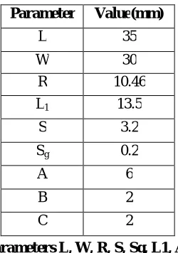
Figure 4: Parameter of an antenna design.
Parametric view of designing antenna is shown in Figure 4. The dimension of each part of circular monopole antenna SRR, ground and the patch are shown above. Length and width of the antenna and each part are shown by
using parameters L, W, R, S, Sg, L1, a, b and c. In thisFR4 material substrate is used.The lengthandwidth of CPWfeed
ISSN (Print) : 2320 – 3765 ISSN (Online): 2278 – 8875
I
nternational
J
ournal of
A
dvanced
R
esearch in
E
lectrical,
E
lectronics and
I
nstrumentation
E
ngineering
(A High Impact Factor, Monthly, Peer Reviewed Journal)
Website: www.ijareeie.com
Vol. 6, Issue 10, October 2017
Table 1: Parameters L, W, R, S, Sg, L1, A, B and C.
The propagating EM signal along the CPW feed line having its magnetic field oriented along the axis. The SRR induces an electromotive force which turninduces a current oscillating between the two rings of the SRR. This oscillating current between two rings yields a resonance, which determined by the SRR’s geometry and prohibits signal propagation at that frequency. This resonance frequency can be determined from the equivalent current approach demonstrated in which involves calculation of distributed capacitance between the rings of the SRR and total inductance of the SRR.The SRR resonance frequency can calculate from the following section. SRR resonance frequency calculated by formulae,
0
1 / 2 / 1
f
LC
(1)The notch characteristics of the SRR loaded CPW feed circular monopole antenna can be calculate using the following formulae:
1/ 2
(
1) / 2 (
1) / 2(1 12(
))
eff r r
H
f
w
(2)Where, εeffis the effective dielectric constant and εr is 4.4 as the substrate is FR4, h is 1.6 mm having height of the substrate. By using, all values εeff can be calculate.
III. SIMULATED RESULTS AND DISCUSSIION
ACPW fed circular monopole UWB antenna to obtain single frequency notch is simulated on FR4 substrate having
thickness h=1.6 mm and dielectric constant Er=4.4. This prototypewas designed and simulated on FR4 material using a
commercial EM simulator that is HFSS.
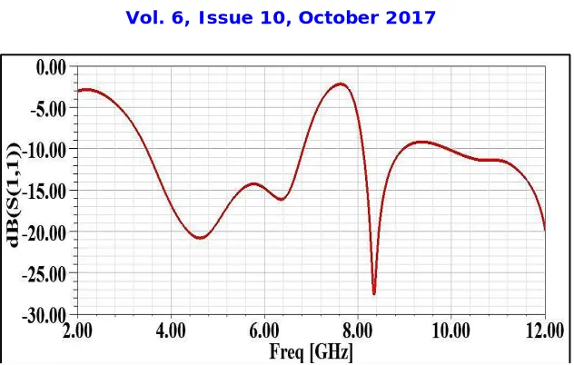
UWB antenna operates in the frequency range 3.1 to 10.6GHz.The S11of the CMA shows in Figure 2 should be less than -10 dB to get the stable radiation characteristics throughout entire bandwidth In Figure 5 shows the frequency response of the circular monopole antenna with dip of the notch characteristics below from -10dB for the entire bandwidth (3.1 GHz to 10.6GHz). The current oscillating between theSRR exhibits filter characteristics, which determined by SRR geometry and desired notch frequency. The rectangular shaped SRR is placed on the patch of the circular monopole antenna and arranged side-by-side of the CPW feed line and due to this notch generated [7].
Parameter Value(mm)
L 35
W 30
R 10.46
L1 13.5
S 3.2
Sg 0.2
A 6
B 2
ISSN (Print) : 2320 – 3765 ISSN (Online): 2278 – 8875
I
nternational
J
ournal of
A
dvanced
R
esearch in
E
lectrical,
E
lectronics and
I
nstrumentation
E
ngineering
(A High Impact Factor, Monthly, Peer Reviewed Journal)
Website: www.ijareeie.com
Vol. 6, Issue 10, October 2017
Figure 5:Simulated return loss (S11) of the SRR loaded CPW fed UWB circular monopole antenna with notch frequency.
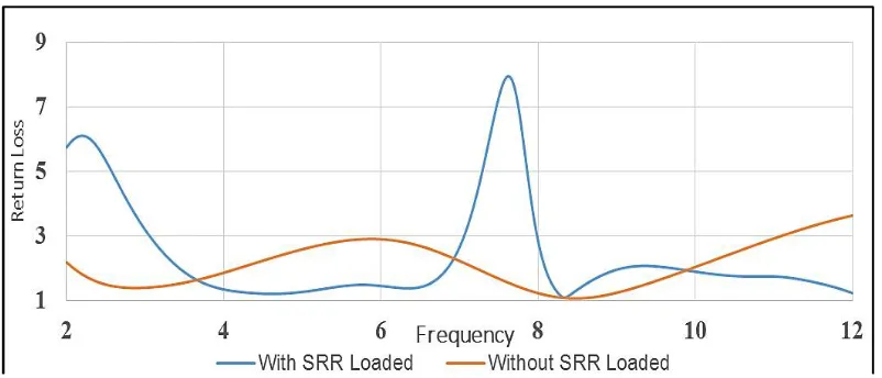
The notch of X-band satellite communication is generated because of SRR has 8.23 GHz frequency notch and -28.83 dB (8.01 to 8.57 GHz) return loss. Moreover, the X-band satellite communication is reserve for armament services.This is the combined return loss graph withand without SRR loaded (Figures6 and 7) (Table 2).
ISSN (Print) : 2320 – 3765 ISSN (Online): 2278 – 8875
I
nternational
J
ournal of
A
dvanced
R
esearch in
E
lectrical,
E
lectronics and
I
nstrumentation
E
ngineering
(A High Impact Factor, Monthly, Peer Reviewed Journal)
Website: www.ijareeie.com
Vol. 6, Issue 10, October 2017
Figure 7: Simulated return loss with different SRR values.
Value Return Loss
0.3 -22dB at 4.5 GHz
0.4 -21dB at 4.5GHz
0.5 -22dB at 4.3GHz
Table 2: Different values of SRR.
The VSWR plot of the SRR loaded circular monopole antenna is shown in Figure 8. The Figure 8 observed that VSWR values are less than 2 for entire bandwidth except 7.34 GHz notch frequency.
Figure 8: Simulated VSWR of the antenna.
ISSN (Print) : 2320 – 3765 ISSN (Online): 2278 – 8875
I
nternational
J
ournal of
A
dvanced
R
esearch in
E
lectrical,
E
lectronics and
I
nstrumentation
E
ngineering
(A High Impact Factor, Monthly, Peer Reviewed Journal)
Website: www.ijareeie.com
Vol. 6, Issue 10, October 2017
Figure 9: Simulated VSWR with and without SRR loaded.
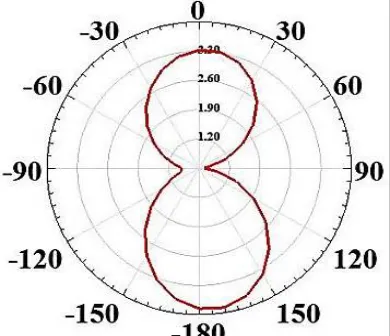
IV. RADIATION PATTERN WITH SRR
Figure 10: Radiation pattern of the E and H plane directional pattern.
ISSN (Print) : 2320 – 3765 ISSN (Online): 2278 – 8875
I
nternational
J
ournal of
A
dvanced
R
esearch in
E
lectrical,
E
lectronics and
I
nstrumentation
E
ngineering
(A High Impact Factor, Monthly, Peer Reviewed Journal)
Website: www.ijareeie.com
Vol. 6, Issue 10, October 2017
Figure 11: Radiation pattern of E-plane.
V. RADIATION PATTERN OF WITHOUT SRR
The center frequency of desired antenna is 4.3GHz, the whole antenna will support on the center frequency at 4.3GHz,
and the bandwidth is 3.1 GHz to 10.6 GHz (Ultra-wideband frequency).
TheRadiationpatternoftheproposedantennafor4.3GHzisshowninFigure 10. The antenna design shows a directional radiation pattern, in other words, an antenna radiate in a particular direction and operate its own center frequency at 4.3GHz. TheRadiationpatternoftheproposedantennafor omnidirectional pattern and directional pattern is shown in
Figure 11. Radiation pattern for omnidirectional at (Phi= 0°) ∅=0° and directional pattern at (Phi= 90°) ∅=90°.
Omnidirectional pattern has plotted on an XZ - Plane and the directional pattern has plotted on a YZ - plane. In Figure 10, the radiation pattern of directional antenna is also known Dipole pattern (E- Plane) and the omnidirectional pattern is on H-Plane. In Figure 11, the radiation patterns are on the EH – plane [8-12].
ISSN (Print) : 2320 – 3765 ISSN (Online): 2278 – 8875
I
nternational
J
ournal of
A
dvanced
R
esearch in
E
lectrical,
E
lectronics and
I
nstrumentation
E
ngineering
(A High Impact Factor, Monthly, Peer Reviewed Journal)
Website: www.ijareeie.com
Vol. 6, Issue 10, October 2017
Figure 13: Radiation pattern of E& H plane without SRR loaded.
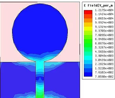
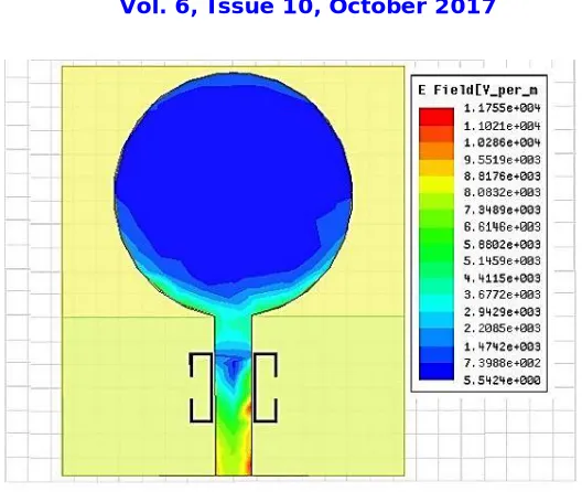
VI. CURRENT DISTRIBUTION WITH SRR
Current distribution with srr can be further investigated in terms of leaky-wave interaction between the ground plane and the feed line and the radiating patch. The leaky wave was presented through the leakage current distribution as shown in Figures 12-15. It can be seen that the leakage current distribution from the ground plane is weaker. As a result, the operational characteristics of the antenna become better [13].
ISSN (Print) : 2320 – 3765 ISSN (Online): 2278 – 8875
I
nternational
J
ournal of
A
dvanced
R
esearch in
E
lectrical,
E
lectronics and
I
nstrumentation
E
ngineering
(A High Impact Factor, Monthly, Peer Reviewed Journal)
Website: www.ijareeie.com
Vol. 6, Issue 10, October 2017
Figure 15: Current distribution with SRR.
VII. CONCLUSION
A CPW fed circular monopole UWB antenna loaded with rectangular shaped SRRs with single frequency notch characteristics on FR4 substrate has been proposed and presented in this work.The work with precise positioning of the SRR place on the side-by-side of the CPW feed line.The proposed antenna is able to cover the entire UWB spectrum except at 8.23GHz which obtained by SRR. The electromagnetic coupling between the CPW and SRR at its resonance frequency yields the desired frequency notch. Since, the antenna dimension and SRR dimensions are independent of each other,SRR dimension only depends on the notching frequency. The notch frequency can be customized to the desired value by changing the SRR dimensions.
REFERENCES
[1] Siddiqui JY; Saha C; Antar YMM; Compact SRR Loaded UWB Circular Monopole Antenna with Frequency Notch Characteristics. IEEE transactions on antennas and propagation 2014; 62:4015-4020.
[2]Wang P; Wen GJ; Huang YJ; Sun YH; Compact CPW-fed planar monopole antenna with distinct triple bands for Wi-Fi/WiMAX applications. ElectronLet2012; 48: 357–359.
[3]Nguyen DT; Lee DH; Park HC; Very compact printed triple band-notched UWB antenna with quarter-wavelength slots. IEEE Antennas Wireless PropagLet 2012; 11: 411–414.
[4]Tang MC; Xiao S, Deng T, Wang D, Guan J, et al. Compact UWB antenna with multiple band-notches for WiMAX and WLAN. IEEE Trans Antennas Propag 2011; 59: 1372–1376.
[5]Zhang LN, Zhong SS, Du CZ,Chen JN, Compact UWB planar monopole antenna with band-notch function Microw Opt Technol Lett 2009; 51: 1908–1911.
[6]Peng L; Ruan CL; UWB band-notched monopole antenna design using electromagnetic-bandgap structures. IEEE Trans Microw Theory Tech 2011; 59: 1074–1081.
[7]Liu WC; Dual wideband coplanar waveguide-fed notched antennas with asymmetrical grounds for multi-band wireless application. IET Microw Antennas Propag2007; 5: 980–985.
[8]Liang J; Guo L; Chiau CC; Chen X; Parini CG;Study of CPW-fed circular disc monopole antenna for ultra-wideband applications. IEEE Proc Microw Antennas Propagat 2005; 52: 520–526.
[9]Liu HW,Ku CH; Yang CF; Novel CPW-fed planar monopole antenna for WiMAX/WLAN applications,” IEEE Antennas Wireless Propag. Lett2010; 9: 240–243.
ISSN (Print) : 2320 – 3765 ISSN (Online): 2278 – 8875
I
nternational
J
ournal of
A
dvanced
R
esearch in
E
lectrical,
E
lectronics and
I
nstrumentation
E
ngineering
(A High Impact Factor, Monthly, Peer Reviewed Journal)
Website: www.ijareeie.com
Vol. 6, Issue 10, October 2017
[11]Gao GPL; Mei ZL; Li BN; Novel circular slot UWB antenna with dual band-notched characteristic. Progress in Electromagnetic Research C 2010; 15: 49-63.
[12]Kim KH, Park SO, Design of the band-rejected UWBantenna with the ring-shaped parasitic patch. Microwave and Optical Technology Letters2006; 48: 1310–1313.