A Novel Method for UVM & BIST Using Low Power Test
Pattern Generator
Boggarapu Kantha Rao
1; Ch.swathi
2& Dr. Murali Malijeddi
3 1HOD &Assoc Prof, Medha Institute of Science and Technology for Women [email protected]
2
M-Tech ECE Department, Medha Institute of Science and Technology for Women 3
Principal and Professor in the Department of ECE in Medha Institute of Science and Technology for Women
Abstract
This project describes a design of low-power (LP) programmable generator capable of producing pseudo random test pattern generator (PRPG) with desired toggling levels, code coverage and functional coverage using Universal Verification methodology (UVM). It is comprised of a linear finite state machine (a linear feedback shift register (LFSR) or a ring generator) driving an appropriate phase shifter and it comes with a number of features allowing this device to produce binary sequences. In the Built In-Logic-Block Observation (BILBO), the require consideration of time and power is not desirable.so we are introducing a self-testing using MISR and parallel SRSG (STUMPS) architecture. Furthermore, this project proposes an LP test pattern generator comparison method that allows shaping the test power envelope in a fully predictable, accurate, and flexible fashion by adapting the STUMPS-based logic BIST infrastructure over conventional method. The proposed LPPRPG is designed using Verilog HDL and functional coverage is verified by using System Verilog and UVM.
Keywords:
built-in–self-test (BIST); LP (low-power) test; pseudo random pattern generator (PRPG); STUMPS; System Verilog; Universal Verification Methodology (UVM).1.
Introduction
As the complexity of VLSI circuits constantly increases, there is a need of a built-in self-test (BIST) to be used. Built-in self-test enables the chip to test itself and to evaluate the circuit’s response. There have been proposed many BIST equipment design methods. In most of the state-of-the-art methods some kind of a pseudorandom pattern generator (PRPG) is used to produce vectors to test the circuit. These vectors are applied to the circuit either as they are, or the vectors are modified by some additional circuitry in order to obtain better functional coverage. Patterns generated by simple LFSRs or CA often
external costly Automatic Test Equipment (ATE). In addition, BIST can provide at speed, in system testing of the Circuit-Under Test (CUT).
1.1.Linear Feedback Shift Register(LFSR)
Linear Feedback shift registers (LFSRs) are commonly used in data-compression circuits implementing a signature analysis technique
called cyclic-redundancy check (CRC).
Autonomous LFSRs are used in applications requiring pseudo-random binary numbers. For example, an autonomous LFSR can be a random pattern generator providing stimulus patterns to a circuit. The response to these patterns can be compared to the circuit’s expected response and thereby reveal the presence of an internal fault. The autonomous LFSR shown in Figure 3.2 has binary tap coefficients C1,………CN that determine whether Y [N] is connected directly to the input of the left most stage.
In general if CN-j+1 = 1, then the input to stage j is formed as the exclusive-or of Y [j - 1] and Y [N], for j=2, . . . . .N. Otherwise, the input to stage j is the output of stage j-1-Y[j] <= Y [j - 1]. The vector of tap coefficients determines coefficients of the characteristics polynomial of the LSFR, which characterize its cyclic nature. The characteristic polynomial determines the period of the register (the number of cycles before a pattern repeats).
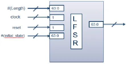
Fig 1: Pin Description of Linear Feedback Shift Register.
Use of linear feedback shift register (LFSR) is being studied extensively by engineers, designers and researchers working in testing design for testability and built-in self-test Environments. LFSRs are rather attractive structures for use in these environments fir some of the following reasons:
1) LFSRs have a simple and fairly regular structure,
2) Their shift property is easily integratable in the scan design environment,
3) They are capable of generating exhaustive and / or random vectors, and
4) Their error correction and error detection properties make them prime candidates for
signature analysis applications.
This is accomplished by using a multiple input signature register (MISR or MSR) which is a type of LFSR. A standard LFSR has a single XOR or XNOR gate where the input of the gate is connected to several "taps" and the output is connected to the input of the first flip-flop. A MISR has the same structure; however, the input to every flip-flop is fed through an XOR/XNOR gate. For example, a four bit MISR has a four-bit parallel output and a four-bit parallel input. The input of the first flip-flop is XOR/Oxnard with parallel input bit zero and the "taps." Every other flip-flop input is XOR/Oxnard with the preceding flip-flop output and the corresponding parallel input bit. Consequently, the next state of the MISR is dependent on the last several states opposed to just the current state. Therefore, a MISR will always generate the same golden signature given that input sequence is the same every time.
2. Related Work
2.1 Basic ArchitectureThe main challenging areas in VLSI are performance, cost, testing, area, reliability and power. The demand for portable computing
devices and communications system are
increasing rapidly. These applications require low power dissipation for VLSI circuits. The power dissipation during test mode is 200% more than in normal mode. Hence it is important aspect to optimize power during testing. Power optimization is one of the main challenges. There are various factors that affect the cost of chip like packaging, application, testing etc. In VLSI, according to thumb rule 5000 of the total integrated circuits cost is due to testing.
During testing two key challenges are:
Cost of testing that can't be scaled.
Engineering effort for generating test
vectors
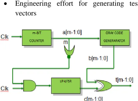
Fig 3: Low-Power Linear feedback shift register (LP-LFSR).
There are main two sources of power dissipation in digital circuits; these are static and dynamic power dissipation. Static power dissipation is mainly due to leakage current and its contribution to total power dissipation is very small [2]. Dynamic power dissipation is due to switching i.e. the power consumed due to short circuit current flow and charging of load capacitances is given by equation:
mode. To test large circuit, circuits are partitioned to save the test time but this parallel testing result in excessive energy and power dissipation.
Due to the lack of at-speed equipment
availability, delay is introduced in the circuit during testing. This cause power dissipation.
In this successive functional input vectors
applied to a given circuit in normal mode have a significant correlation, while the correlation between consecutive test patterns can be very low. This can cause large switching activity in the circuit during test then that during its normal operation. During testing large power is dissipated than in the normal mode.
3. Implementation
Testing of integrated circuits (ICs) is of crucial importance to ensure a high level of quality in product functionality in both commercially and privately produced products. The impact of testing affects areas of manufacturing as well as those involved in design. Given this range of design involvement, how to go about best achieving a high level of confidence in IC operation is a major concern. This desire to attain a high quality level must be tempered with the cost and time involved in this process. These two design considerations are at constant odds. It is with both goals in mind (effectiveness vs. cost/time) that Built-In-Self Test (BIST) has become a major design consideration in Design-For-Testability (DFT) methods.
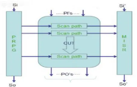
The self-testing using MISR and parallel SRSG (STUMPS) architecture is shown in below figure. The STUMPS architecture introduced by Bardell and McAnney 1982, 1984. It was originally applied at the board level, and
subsequently at the chip level.it has the following attributes:
Centralized and separated BIST
architecture;
Multiple scan paths;
No boundary scan
The scan paths are driven in parallel by a PRPG, and the signature is generated in parallel from each scan path using a MISR. At the board level, each scan path corresponds to the scan path in a separate chip, at the chip level each scan path is just one segment of the entire scan path of a chip. The use of multiple scan paths leads to a significant reduction in test time. Since the scan paths may be of different lengths, the PRPG is run for K clock cycles to load up the scan paths, where K is the length of the longest scan path. For short scan paths, some of the data generated by the PRPG flow over into the MISR. When this approach is applied at the board level to chips designed with a scan path, then the PRPG and the MISR can be combined into a special-purpose test chip, which must be added to the board.
Fig 4: Self-testing using MISR and parallel SRSG (STUMPS)
LFSR is used in the PRPG, then Qi(t)=Qi-1(t-1). Hence data is one scan path are a shifted version of data in another scan path. To avoid this situation, a type 2 LFSR can be used .the external logic must be tested via ATE or by adding boundary scan registers.
4. Experimental Work
TheapproachpresentedinSectionIVhasbeenvalidat edbyexperimentsrunonfivedifferentscanarchitect ures(203×300,122×104,84×416,128×353,160×54 1)usedinfiveindustrialdesigns,andwitha33bitringg eneratorimplementingaprimitivepolynomial x33+x25+x16+x8+1 and feeding33-input phase shifter for 10000 pseudo random test patterns.
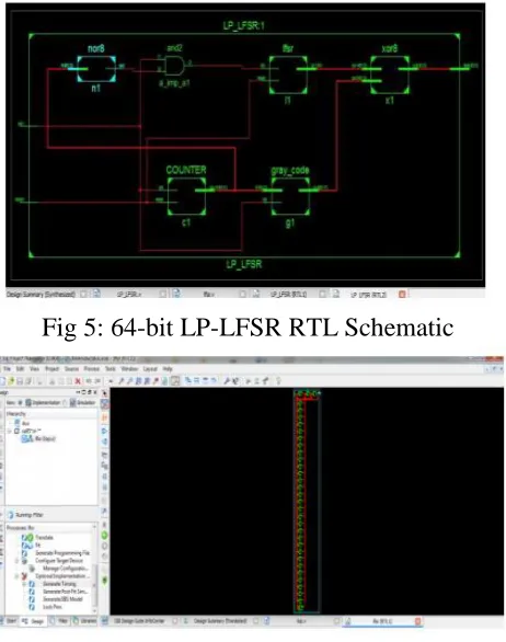
Fig 5: 64-bit LP-LFSR RTL Schematic
Fig 6:64-bit conventional LFSR schematic
5. Conclusion
SOC designs are making a rapid shift from mostly digital to mixed signal including millions of user defined logic gates and dozens of IP
(Core as well as I/O based). IC Verification and Test strategy needs to include advanced controllers and pattern generators for testing digital as well as analog components of the chip. Pattern generation inside the chip is well known to cause increase in the power consumption of the IC during the manufacturing test. New design and test techniques need to be investigated to keep this increase in the power consumption by the chip as minimum as possible. The availability of advanced manufacturing process rules in the design/verification libraries and tool flow methodologies is mandating the IC front-end designers to verify the manufacturability of the chip much in advance in the design process . Therefore development of the new SOC DFT techniques needs to be compliant with the advanced DFM rules.
6. References
[1] A. S. Abu-Issa and S. F. Quigley, ―Bit-swapping LFSR for low-power BIST,‖ Electron. Lett., vol. 44, no. 6, pp. 401–402, Mar.2013.
[2] [K2] IEEE Std. 1364-1995, IEEE Standard Hardware Description Language Based on the Verilog¨ HardwareDescription Language 1995.
ISBN 0-7381-3065-6. IEEE Product No.
WE94418-TBR.
[3] A. Sagahyroon, G. Lakkaraju and M.
karunaratne, "A Functional Verification
Environment,", Circuits and Systems
Symposium. 48th Midwest, 108-111 Vol.1, 2014
[5] A. Jas, C. V. Krishna, and N. A. Touba, ―Weighted pseudorandom hybrid BIST,‖ IEEE Trans. Very Large Scale Integr. (VLSI) Syst., vol. 12, no. 12, pp. 1277–1283, Dec. 2004.
[6] R. Kapur, S. Mitra, and T. W. Williams, ―Historical perspective on scan compression,‖ IEEE Design Test, vol. 25, no. 2, pp. 114–120, Mar./Apr. 2008.
[7] B. Koenemann, ―LFSR-coded test patterns for scan designs,‖ in Proc.Eur. Test Conf. (ETC), 1991, pp. 237–242.
[8] Y. Kim, M.-H. Yang, Y. Lee, and S. Kang, ―A new low power test pattern generator using a transition monitoring window based on BIST architecture,‖ in Proc. Asian Test Symp. (ATS), Dec. 2005, pp. 230–235.
[9] C. V. Krishna and N. A. Touba, ―Reducing test data volume using LFSR reseeding with seed compression,‖ in Proc. Int. Test Conf. (ITC), 2002, pp. 321–330.
[10] C. V. Krishna and N. A. Touba, ―Hybrid BIST using an incrementally guided LFSR,‖ in Proc. 18th IEEE Int. Symp. Defect Fault Tolerance(DFT) VLSI Syst., Nov. 2003, pp. 217–224
[11] IEEE IEEE Standard for SystemVerilog — Unifi ed Hardware Design, Specifi cation, and Verifi cation Language . New York: IEEE 2009 (a.k.a. SystemVerilog Language Reference Manual,or LRM.)
[12] IEEE Standard Verilog Hardware Design, Description Language . New York: IEEE 2001 Rich, Dave Are SystemVerilog Program Blocks Needed?
Authors Profiles
Boggarapu Kantha Rao
HOD &Assoc Prof, Medha Institute of
Scienceand Technology for Women,
India,B.KANTHA RAO received the B.Tech. Degree in Electronics and Communication
Engineering from Jawaharlal Nehru
Technological University, Hyderabad in 2006 and M.Tech in EMBEDDED SYSTEMS from Jawaharlal Nehru Technological University, Hyderabad in 2010, is a faculty member in the department of Electronics and Communication Engineering, Medha Institute of Science and
Technology for Women, Khammam and
presently working as Associate Professor. His research interests include Embedded systems,
VLSI Design. E-mail: [email protected].
Medha Institute of Scienceand Technology for Women, India,
Dr. Murali Malijeddi
Mr.mr.muralimalijeddi has completed his PhD
from Andhra University Under Guidance of Prof. Dr. G.S.N Raju, Vice-Chancellor, Andhra
University in Antennas and Signal Processing .
As a Principal and Professor in the Department of ECE in Medha Institute of Science and
Technology for Women KHAMMAM,