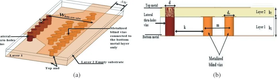
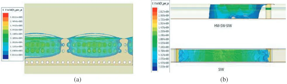
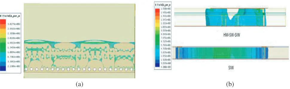
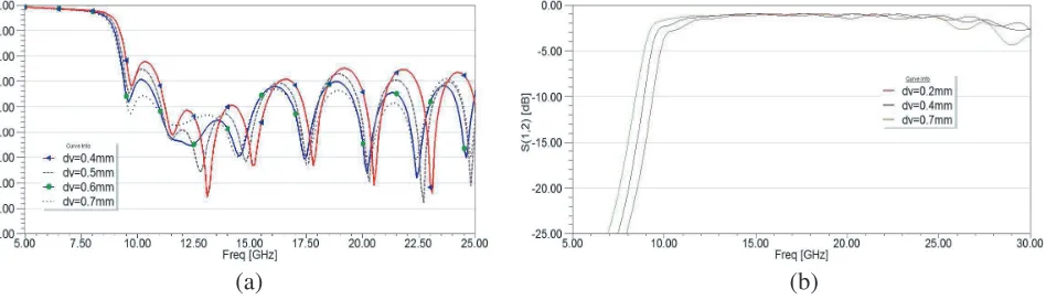
Half-Mode Slow-Wave Substrate Integrated Waveguide Analysis
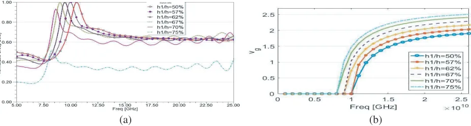
Mohamad Khalil1, 2, Mahmoud Kamarei1, *, Jalal Jomaah2, Hussam Ayad2, and Majida Fadlallah2
Abstract—Design of a compact Substrate Integrated Waveguide (SIW) transmission line is presented in this paper. The main parameters of SIW were parametrically studied, and final designed component was fabricated and measured, which showed very good matching (near 90%) with simulations, demonstrating significant miniaturization factor. The miniaturization was done using Half-Mode (HM) and Slow-Wave (SW) principles together. It was found that the HM-SW method for SIW miniaturization reduced the SIW surface area with a remarkable factor value (70%) while maintaining acceptable characteristics compared to the original SIW. In fact, HM technique reduced 40% the lateral dimension of the SIW, and using the SW technique allowed 30% of size reduction added to the HM principle. Furthermore, a proper microstrip to HM-SW-SIW tapered transition was designed, which showed a return loss decrease between 3 dB and 7.5 dB, as well as facilitating measurement. On the other hand, the proposed transmission line could lead to a size reduction of 30% compared to the HM-SIW miniaturization technique. The HM-SW-SIW transmission line concept presented in this paper can be used to design other compact SIW components such as bandpass filters, couplers, and power divider.
1. INTRODUCTION
The number of papers published since the introduction of SIW has been increasing in a cumulative way in the last decade [1]. This shows the importance of SIW in microwave and millimeter-wave systems. Several reasons have led to investigations in such a type of technology (e.g., high quality factor, electromagnetic shielding, and wide bandwidth while having the possibility of integration with other integrated circuits). These advantages are missed in the microstrip technology. The main disadvantage of this new transmission line is a larger foot print than the microstrip technology.
Different research works have focused on SIW miniaturization; for example, multilayer SIW technique was applied on a Butler-matrix in [2] and [3] in order to reduce the area by stacking the components on each other. Furthermore, [4–6] presented a folded technique for SIW miniaturization, and a 50% of size reduction was demonstrated compared to the conventional SIW. On the other hand, ridged SIW was proposed in [7] and [8], and a 40% of size reduction along with a broad bandwidth was achieved. In [9], the Half-Mode SIW (HM-SIW) was presented, which reduces the SIW size by half while maintaining good characteristics and low complexity. In [10] a combination of the HM and folded techniques was used, and a significant reduction in size of a 3-dB coupler was observed. Topologies mentioned above are all based on double-layer technology in order to increase the miniaturization factor, except the HM principle. Also these techniques focus only on reducing the width of the conventional SIW, by decreasing the cutoff frequency, using the symmetric plane along the transmission direction that is equivalent to a magnetic wall or stacking components on each other.
The SW concept was used in [11]. This concept is widely used in planar transmission lines and components for improving their characteristics. However, it is recently applied to SIW technology in
Received 4 January 2017, Accepted 16 July 2017, Scheduled 2 October 2017
* Corresponding author: Mahmoud Kamarei ([email protected]).
1 Department of Electrical and Computer Engineering, University of Tehran, Iran. 2 Physics Department, Lebanese University,
order to reduce both the lateral and longitudinal dimensions of the transmission line by decreasing the cutoff frequency and electrical length, respectively, unlike previously mentioned techniques that reduce only the width. Thus, additional increase in the miniaturization factor is achieved. Niembro-Mart´ın et al. [11] demonstrated that SW concept reduces the surface of the conventional SIW by 40%. This concept was also applied to a leaky wave antenna in [12]. Recently, [13] showed that combining the SW with HM techniques would reduce conventional SIW dimensions with a remarkable factor (by 70%) in comparison with original SIW, thus a higher miniaturization factor would be achieved. However, only scattering parameters were presented in [13] in order to demonstrate the HM-SW-SIW concept.
In this paper, more details about the characteristics of the HM-SW-SIW concept are presented. In addition to the electromagnetic field distribution showing field separation, group delay and group velocity demonstrating the SW effect are also shown. A comparison with HM-SIW using different substrates is presented. Moreover, the fabricated component is measured and compared to simulation results; a good matching is achieved.
This paper is organized as follows. Section 2 deals with HM-SW-SIW concept and EM-field distribution. Parametric study, tapered transition design and comparison with other transmission line are also found in this section. Section 3 is dedicated to HM-SW-SIW prototype and measurement results. Finally, a conclusion is given in Section 4.
2. HM-SW-SIW CONCEPT
2.1. Transmission Line Configuration
The 3-D and cross-sectional views of the proposed two-layer HM-SW-SIW concept are shown in Figure 1. It can be observed that the lateral through-holes vias are connected between the top metal layer and bottom metal layer from one side defining the HM-SIW lateral dimension. Two rows of metalized blind vias inside the HM-SIW are also connected to the bottom metal layer only inducing SW effect. HM-SIW and SW together define the HM-SW-SIW concept in a double-layer technology. Moreover, a microstrip to HM-SW-SIW tapered transition is used for optimizing the performance and easier measurements.
(a) (b)
Figure 1. HM-SW-SIW representation: (a) 3-D view, and (b) cross-sectional view.
The HM-SW-SIW transmission line design is divided into three steps. First, we start from a simple SIW design following the method given in [14]; thus we obtain Wsiw = 6.92 mm for fc10 = 12.7 GHz
using RO4003C as substrate with heighth= 0.508 mm.
Second, the HM principle is applied to the SIW. The HM-SIW as explained in [9] is based on the symmetry of electric field to the magnetic wall, i.e., we can use only one half of the SIW without altering its property and thus reducing the lateral dimension of the SIW to half while maintaining good characteristics. Thus cutting the SIW into half along its longitudinal symmetry planes forms the HM-SIW having a width significantly reduced compared to the conventional HM-SIW. The width of HM-HM-SIW equals Whm-siw = W2siw, and its effective width,Weff-hm-siw, is calculated using Equation (1) [15]:
where, the additional width, ΔW, which needs to be determined using Equation (2), accounts for the effect of the fringing fields, and is a function of the width, Wsiw/2, of the waveguide height h and the substrate permittivity r [15]:
ΔW h =
0.05 + 0.30
r
×ln
0.79×W
2
siw/2
h3 +
104×Wsiw/2−261
h2 +
38
h + 2.77
(2)
The SIW transmission line width was calculated previously as Wsiw = 6.92 mm and thus ΔW = 0.861 mm.
Finally, the HM-SW-SIW is obtained by inserting blind vias inside the HM-SIW. Now our design is an HM-SW-SIW with two layers (Figure 1). Substrates of layers 1 and 2 are Rogers RO4003C with relative dielectric constantr = 3.55, dielectric loss tangent tangδ= 0.0027 and thicknessh1 = 0.508 mm
and h2 = 0.254 mm, respectively. The top and bottom metal layers are copper with a thickness equal
to 17µm. The total height is obtained as h = h1+h2 +hp = 0.864 mm, where hp is the thickness of
the adhesive film used for bonding substrates of layers 1 and 2, and its width isWhm-sw-siw = 3.46 mm. The spacing and height of blind vias inserted in layer 1 are set in order to have the lowest reflection loss and good miniaturization factor in the longitudinal and lateral dimensions based on the analysis done in Section 2.3. Therefore, two rows of internal metallized blind vias were considered as shown in Figure 1. The diameter dv of the blind vias and the center-to-center spacing between two adjacent internal vias were fixed to dv = 0.4 mm and m = 0.8 mm, respectively. In the longitudinal direction, the center-to-center spacing between two adjacent lateral through-holes vias was fixed to s= 0.8 mm, their diameter fixed to d = 0.4 mm, and the distance between lateral wall and blind vias was set to
k= 1.3 mm (Figure 1(b)).
2.2. Field Distribution and SW Effect
According to [11, 13], the purpose of inserting blind vias inside the SIW is to confine the electric field in the upper layer, thus increasing the effective permittivity and decreasing the cutoff frequency. On the other hand, for a specified periodicity of blind vias, the electric and magnetic fields should be decoupled. Thus, magnetic field will be held in the first layer creating the SW effect and decreasing the electrical length of the transmission line. In order to demonstrate the SW effect, full-wave EM simulation of the proposed design was carried out using HFSS [16].
Top and cross-sectional views of the electric and magnetic fields of the fundamental mode TE10
at 13 GHz were extracted, and the results are shown in Figures 2 and 3. As shown in Figures 2(a) and 2(b), the electric field is confined in the upper layer, and as shown in Figures 3(a) and 3(b), the magnetic field is held in the first layer between the blind vias. Thus, a spatial separation of the electric and magnetic fields is well obtained producing the SW effect. EM-field distribution comparison between HM-SW-SIW and SIW structure is also shown in Figures 2(b) and 3(b). It is easy to notice that the
(a) (b)
(a) (b)
Figure 3. (a) Magnitude top view ofH-field distribution. (b) Magnitude cross-sectional view ofH-field distribution for the HM-SW-SIW and SIW.
fundamental mode in the HM-SW-SIW is quite similar to half of the dominant quasi-TE10mode in the
SIW confined in layer 2 between the top of blind vias and the top metal layer.
TheH-field is well distributed in layer 1 between the blind vias, in comparison to the SIW where the H-field is distributed between the lateral through-hole vias walls and the top and bottom metal layers [see Figure 3(b)].
A simple equation can be used for the initial estimation of the HM-SW-SIW transmission line parameters [17]. Cutoff frequency can be determined using Equation (3):
f chm-sw-siw = c0
4×Whm-siw× √εreff
(3)
whereεreff can be predicted using [18].
From the definition of the guided wavelength,λg can be obtained using Equation (4):
λg = λa
1−
λa
λc
2 (4)
whereλa is the wavelength having an effective dielectric constant εreff, andλc = 4×Whm-siw.
Furthermore, normalized group velocity in Equation (5) can be used in order to predict the percentage of electrical length reduction:
vg
c = λa
λg =
εreff ×
1−
f chm-sw-siw
f
2
(5)
Using Equations (3) and (5), it is possible to accomplish the parametric study done in Section 2.3.
2.3. Parametric Study
As mentioned, inserting blind vias in the first layer will separate EM fields, thus the transmission line’s performance is dependent on the ratio of the first layer thickness and the waveguide thickness, as well as on the blind vias diameter. Therefore, in order to demonstrate the decrease of both cutoff frequency and electrical length in the presence of internal metalized blind vias-holes, effect of different waveguide thicknesses and blind vias diameter variations is examined in this section. The thickness variation effect of the first layer (h1) is shown in Figure 4. It is observed in Figure 4(a) from theS-parameters how the
cutoff frequency is decreased while increasing the thickness ratio h1/hand maintaining a fixed lateral
(a) (b)
Figure 4. First layer thickness variation h1 of the HM-SW-SIW with two rows of blind vias: (a)
reflection coefficient, and (b) insertion loss.
(a) (b)
Figure 5. Blind vias diameter variation dv of the HM-SW-SIW with two rows of blind vias: (a) reflection coefficient, and (b) insertion loss.
be obtained. On the other hand, both the return loss and the insertion loss increase with the increase of the thickness ratio (Figure 4), and this effect is normal due to the increase of the conduction loss.
Figure 5 shows the blind vias diameter variation for a transmission line with a thickness ratio of h1/h = 62%. There is no significant effect on the cutoff frequency when modifying the blind vias’
diameter as shown in Figure 5(a). Also both of the return loss and the insertion loss are almost unaffected (Figure 5). Thus the main miniaturization effect in lateral dimension is due to the waveguide thickness. On the other hand, group delay is an important factor showing the phase linearity of the transmission line, and group velocity demonstrates the SW effect and the reduction of the electrical length of the transmission line. Therefore, the effect of blind vias on group delay and group velocity is also checked and shown in Figure 6. It can be observed from Figure 6(a) that increasing the thickness ratio increases the instability of the group delay due to discontinuities introduced by the blind vias, whereas SW effect increases which in turn, decreases the electrical length of the transmission line (Figure 6(b)) due to increase of the electric and magnetic fields’ decoupling.
(a) (b)
Figure 6. (a) Group delay, and (b) group velocity (slow wave factor) of the HM-SW-SIW.
(a) (b)
0.2 0.3 0.4 0.5 0.6 0.7
blind vias diameter (mm)
0.2 0.3 0.4 0.5 0.6 0.7
blind vias diameter (mm) 0.55
0.52
0.49
0.46
0.43
0.4
v
/
c
g
0
0.8
0.77
0.74
0.71
0.68
0.65
f
/
fc-siw
c
-hm
-sw
-siw
Figure 7. (a) Normalized group velocity, and (b) normalized cut-off frequency.
compared to microstrip lines or CPWs, this is similar to a decrease of the inductance of the transmission line, leading to group velocity decrease. Thus, a certain blind vias periodicity and diameter must be respected in order to preserve the SW effect, hence reducing electrical length and width simultaneously. Finally, based on the previous analysis, in order to reduce the area of SIW, a compromise has to be considered among the lowest cutoff frequency, group velocity acceptableS-parameters, and group delay. High thickness ratio could effectively reduce the cutoff frequency and group velocity, and consequently reduce lateral and longitudinal dimensions; however, return loss and insertion loss increase, and an unstable group delay is obtained.
2.4. Microstrip to SIW Transition
It is well known that tapered transition shows good performance and covers the entire bandwidth of SIW compared to other types of transitions [19]. Therefore, tapered transition of the conventional SIW is divided into the half, and then blind vias are inserted under the tapering, as shown in Figure 8. Thus, EM field confined in the second layer will propagate efficiently into the HM-SW-SIW. The width (Wtap) and length (Ltap) of the tapering section were optimized in order to obtain the best return loss over the full waveguide bandwidth, and the microstrip part (Wms) was optimized to obtain a 50-Ω characteristic impedance (Wms = 1.95 mm), as shown in Figure 8(b).
Figure 9(a) shows the effect of the internal blind vias’ diameter under the tapered transition on
S11-parameter. It is noticed that return losses are increased with the increase of blind vias’ diameter
(Rv). Their number also affects the return loss level; therefore, the minimal number and diameter of blind vias facilitating the EM propagation having broader bandwidth and lower return loss are chosen.
(a) (b)
Figure 8. HM-SW-SIW microstrip tapered transition: (a) 3-D view, and (b) cross-section view.
(a) (b)
Figure 9. (a) Reflection parameters of the HM-SW-SIW transition alone, and (b)S-parameters of the transmission line with and without tapered transition.
2.5. Comparison with HM-SIW
A comparison between the HM-SW-SIW and two types of HM-SIW is presented in this section. An HM-SIW transmission line is chosen for comparison since it possesses high miniaturization factor while having low profile. The first HM-SIW has a substrate RO4003C with relative permittivity r = 3.55, dissipation factor tanδ = 0.0027 and thickness h = 0.508 mm. The second HM-SIW has a RO6010 substrate with r = 10.2, dissipation factor tanδ = 0.0023 and thickness h = 0.508 mm. In order to carry out accurate comparison, simulation results used for fabrication are selected for comparison. The HM-SIW transmission line is simulated using an SMA connector [see Figure 10(a)].
S-parameters and group delay results are presented in Figures 10 and 11. FromS11-parameter in
Figure 10(b), it can be observed that HM-SW-SIW presents 30% miniaturization factor compared with HM-SIW (RO4003C). It possesses minimum 5 dB lower return loss, with no difference in insertion loss, as shown in Figure 11(a). Concerning group delay shown in Figure 11(b), HM-SW-SIW and HM-SIW
(a) (b)
Figure 10. (a) Top view of the HM-SIW simulated transmission line with SMA connectors, and (b)
(a) (b)
Figure 11. (a) S(1,2) comparison of HM-SW-SIW and HM-SIW transmission lines, and (b) group delay comparison of HM-SW-SIW with HM-SIW transmission lines.
(RO4003C) present similar group delay. On the other hand, comparing the SIW-SIW with HM-SIW (RO6010), the latter has higher miniaturization factor than that of the former. However, return loss is higher than −10 dB in all of the bandwidth. Also insertion loss is near−2 dB with high ripple. Furthermore, as shown in Figure 11(b), HM-SIW (RO6010) presents high and unstable group delay.
Hence, although HM-SIW (RO6010) has high miniaturization factor, it is difficult to be used due to high return loss, insertion loss and dispersion. Although HM-SIW presents low profile, HM-SW-SIW possesses higher miniaturization factor, lower return loss and lower insertion loss, showing a new miniaturization level.
3. SIMULATION AND MEASUREMENT RESULTS
Based on the parametric study presented in Section 2.3, the HM-SW-SIW transmission line considered for fabrication has two rows of blind vias (with dv = 0.4 mm and m = 0.8 mm). Selected substrate is RO4003C with relative dielectric constant r = 3.55, dielectric loss tangent tangδ = 0.0027 for the first and second layers with thicknessesh1 = 0.508 mm andh2 = 0.254 mm, respectively. Copper metal layer
of the substrate has a thickness of 17µm. RO4450F prepreg is used for bonding the two substrates. HM-SW-SIW width,Whm−sw−siw, equals 3.46 mm, leading to the estimated cutoff frequency of 8.9 GHz. Thus, the width decreases by 70% in comparison to the conventional SIW.
Tapered microstrip transition is also considered with metalized blind vias connected to the ground inserted under the transition presenting both easy measurement and better scattering parameter results. As mentioned in Section 2.4, three blind vias were inserted with the diameter of Rv = 0.3 mm, and tapering length and width of Ltap = 1.6 and Wtap = 3.1, respectively. Finally, the microstrip section has a width of Wms = 1.95 mm.
Photographs of the fabricated HM-SW-SIW are shown in Figure 12, and its top and bottom views are shown in Figures 12(a) and 12(b). We can notice that the blind vias under the transition and inside the HM-SW-SIW connected to the bottom metal layer have distance 1.3 mm from the lateral through-holes vias of the HM-SW-SIW.
Measurements were done using Agilent vector network analyzer, with a Short-Open-Load
(a) (b)
(a) (b)
Figure 13. HM-SW-SIW simulation and measurement comparison: (a) reflection coefficient, and (b) transmission coefficient.
(a) (b)
0 0.5 1 1.5 2 2.5
Freq [GHz] x 10 10
0 0.5 1 1.5 2 2.5
v
/
c
g
0
Figure 14. HM-SW-SIW simulation and measurement comparison: (a) group delay, and (b) group velocity.
calibration. Measured S-parameters of the fabricated component were compared with full-wave EM simulations, and the results obtained are shown in Figures 13 and 14. Good matching between measurement and simulation is obtained. Return loss is below 15.7 dB between 8.9 GHz and 21.3 GHz [see Figure 13(a)], and insertion loss is better than−1.5 dB in the whole bandwidth [see Figure 13(b)]. Waveguides are well known with their dispersive nature. In the present research, the measured group delay was 500 ps at 8.9 GHz, which reached 300 ps at 20 GHz as shown on Figure 13(b). Acceptable differences in the delay values of spectral components at the two ending regions of the frequency band of interest was obtained. However, a small decrease in stability was observed due to the discontinuities effect of the blind vias. Finally, the measured and simulated normalized group velocities showed good matching. Also the electrical length was reduced by 50% in comparison to the conventional SIW [see Figure 14(b)].
4. CONCLUSION
In this paper, the HM-SW-SIW transmission line concept was presented. The new miniaturized SIW design presented 70% of size reduction as compared to the conventional SIW, leading to a great size reduction and giving more interest of SIW in lower frequencies. On the other hand, parametric study demonstrated that acceptable characteristics could be obtained while having a good miniaturizing factor. Also comparison with other HM-SIW transmission lines showed that this concept is 30% smaller while maintaining acceptable characteristics. A prototype was fabricated using double-layer PCB technology, and a good matching with the simulation results was obtained.
ACKNOWLEDGMENT
REFERENCES
1. Sahu, A., V. K. Devabhaktuni, R. K. Mishra, and P. H. Aaen, “Recent advances in theory and applications of substrate-integrated waveguides: A review,” International Journal of RF and
Microwave Computer-Aided Engineering, 2015.
2. Djerafi, T. and K. Wu, “Multilayered substrate integrated waveguide 4 × 4 Butler matrix,”
International Journal of RF and Microwave Computer-Aided Engineering, Vol. 22, No. 3, 336–
344, 2012.
3. Cheng, Y. J., C. A. Zhang, and Y. Fan, “Miniaturized multilayer folded substrate integrated waveguide Butler matrix,” Progress In Electromagnetics Research C, Vol. 21, 45–58, 2011.
4. Grigoropoulos, N. and P. R. Young, “Compact folded waveguides,” 34th European Microwave
Conference, Vol. 2, 973–976, IEEE, 2004.
5. Wang, R., L.-S. Wu, and X.-L. Zhou, “Compact folded substrate integrated waveguide cavities and bandpass filter,” Progress In Electromagnetics Research, Vol. 84, 135–147, 2008.
6. Grigoropoulos, N., B. Sanz-Izquierdo, and P. Young, “Substrate integrated folded waveguides (SIFW) and filters,” IEEE Microwave and Wireless Components Letters, Vol. 15, 829–831, Dec. 2005.
7. Bozzi, M., S. Winkler, and K. Wu, “Broadband and compact ridge substrate-integrated waveguides,” IET Microwaves, Antennas &Propagation, Vol. 4, No. 8, 1965–1973, Nov. 2010. 8. Bozzi, M., M. Pasian, and L. Perregrini, “Advanced modeling and design of substrate integrated
waveguide components,” 2014 IEEE International Wireless Symposium (IWS), 1–4, IEEE, 2014. 9. Hong, W., B. Liu, Y. Wang, Q. Lai, H. Tang, X. X. Yin, Y. D. Dong, Y. Zhang, and K. Wu,
“Half mode substrate integrated waveguide: A new guided wave structure for microwave and millimeter wave application,” Joint 31st International Conference on Infrared Millimeter Waves
and 14th International Conference on Teraherz Electronics, 2006, IRMMW-THz 2006, 219–219,
IEEE, 2006.
10. Zhai, G. H., W. Hong, K. Wu, J. X. Chen, P. Chen, J. Wei, and H. J. Tang, “Folded half mode substrate integrated waveguide 3 dB coupler,”IEEE Microwave and Wireless Components Letters, Vol. 18, 512–514, Aug. 2008.
11. Niembro-Martin, A., V. Nasserddine, E. Pistono, H. Issa, A.-L. Franc, T.-P. Vuong, and P. Ferrari, “Slow-wave substrate integrated waveguide,” IEEE Transactions on Microwave Theory
and Techniques, Vol. 62, 2014.
12. Khalil, M., M. Kamarei, J. Jomaah, and H. Ayad, “Compact SIW leaky wave antenna,” 2015 Third International Conference on Technological Advances in Electrical, Electronics and Computer
Engineering (TAEECE), 124–129, Apr. 2015.
13. Khalil, M., M. Kamarei, J. Jomaah, and H. Ayad, “Substrate integrated waveguide miniaturization using slow wave and half mode techniques,” IEEE International Microwave and RF Conference
(IMaRC), 2015.
14. Rayas-Sanchez, J., “An improved EM-based design procedure for single-layer substrate integrated waveguide interconnects with microstrip transitions,” IEEE MTT-S International Microwave
Workshop Series on Signal Integrity and High-Speed Interconnects, 2009, IMWS 2009, 27–30,
Feb. 2009.
15. Lai, Q., C. Fumeaux, W. Hong, and R. Vahldieck, “Characterization of the propagation properties of the half-mode substrate integrated waveguide,” IEEE Transactions on Microwave Theory and
Techniques, Vol. 57, No. 8, 1996–2004, 2009.
16. http://www.ansys.com/products/electronics/ansys-hfss.
17. Collin, R. E.,Foundations for Microwave Engineering, John Wiley & Sons, 2007.
18. Machac, J., “Microstrip line on an artificial dielectric substrate,” IEEE Microwave and Wireless
Components Letters, Vol. 16, No. 7, 416–418, 2006.