University of Windsor University of Windsor
Scholarship at UWindsor
Scholarship at UWindsor
Electronic Theses and Dissertations Theses, Dissertations, and Major Papers
2014
TSV Equivalent Circuit Model using 3D Full-Wave Analysis
TSV Equivalent Circuit Model using 3D Full-Wave Analysis
Zheng GongUniversity of Windsor
Follow this and additional works at: https://scholar.uwindsor.ca/etd
Recommended Citation Recommended Citation
Gong, Zheng, "TSV Equivalent Circuit Model using 3D Full-Wave Analysis" (2014). Electronic Theses and Dissertations. 5238.
https://scholar.uwindsor.ca/etd/5238
This online database contains the full-text of PhD dissertations and Masters’ theses of University of Windsor students from 1954 forward. These documents are made available for personal study and research purposes only, in accordance with the Canadian Copyright Act and the Creative Commons license—CC BY-NC-ND (Attribution, Non-Commercial, No Derivative Works). Under this license, works must always be attributed to the copyright holder (original author), cannot be used for any commercial purposes, and may not be altered. Any other use would require the permission of the copyright holder. Students may inquire about withdrawing their dissertation and/or thesis from this database. For additional inquiries, please contact the repository administrator via email
TSV Equivalent Circuit Model using 3D Full-Wave Analysis
By
Zheng Gong
A Thesis
Submitted to the Faculty of Graduate Studies
through the Department of Electrical and Computer Engineering
in Partial Fulfillment of the Requirements for the Degree of Master of Applied Science
at the University of Windsor
Windsor, Ontario, Canada
2014
TSV Equivalent Circuit Model using 3D Full-Wave Analysis
By
Zheng Gong
APPROVED BY:
______________________________________________ Dr. R. Riahi
Department of Mechanical, Automotive and Materials Engineering
______________________________________________ Dr. M. Mirhassani
Department of Electrical and Computer Engineering
______________________________________________ Dr. R. Rashidzadeh
Department of Electrical and Computer Engineering
______________________________________________ Dr. E. Abdel-Raheem
Department of Electrical and Computer Engineering
iii
DECLARATION OF ORIGINALITY I. Co-Authorship Declaration
I hereby declare that this thesis paper incorporates the outcome of a joint research in collaboration with, and under the supervision of, Dr. Rashid Rashidzadeh, with the review and revision being provided by Dr. Rashid Rashidzadeh.
I am aware of the University of Windsor Senate Policy on Authorship and I certify that I have properly acknowledged the contribution of other researchers to my thesis, and have obtained written permission from each of the co-author(s) to include the above material(s) in my thesis. I certify that, with the above qualification, this thesis, and the research to which it refers, is the product of my own work.
II. Declaration of Previous Publication
This thesis includes one original papers that have been previously published/submitted for publication in peer reviewed conferences, as follows:
Thesis Chapter Publication title/full citation Publication status Design Automation
Conference (DAC), June 1-5, 2014, San Francisco, CA, USA
Work In Progress
Title: TSV Equivalent Circuit Model and Test Solution/ IEEE Trans. Computer-Aided Design of Integrated Circuits and Systems
Prepared for submission
I certify that the above material describes work completed during my registration as graduate student at the University of Windsor.
iv
v ABSTRACT
vii
ACKNOWLEDGEMENTS
viii
TABLE OF CONTENTS
DECLARATION OF ORIGINALITY ... iii
ABSTRACT ...v
DEDICATION ... vi
ACKNOWLEDGEMENTS ... vii
LIST OF TABLES ... xii
LIST OF FIGURES ... xiii
LIST OF ABBREVIATIONS/SYMBOLS ... xvii
Chapter 1Introduction and Background ...1
1.1 Three Dimensional Integrated Circuits ...1
1.1.1 A brief introduction to Three Dimensional Integrated Circuits ...1
1.1.2 Three-dimensional IC fabrication process ...5
1.1.3 TSV structure ...6
1.2 Challenges in Three-dimensional testing methods ...7
1.3 TSV test solutions proposed in the literature ...11
Chapter 2 ...13
Implemented TSV Structure and the Equivalent Circuit ...13
2.1 CAD Tools ...13
2.2 Why HFSS ...14
2.3 Implemented TSV Structure ...14
2.3.1 S-Parameters of the Implemented TSV Structure ...16
2.3.2 Extracted Equivalent Circuit of a TSV ...18
2.4 Analytical Verification ...19
ix
Chapter 3 ...23
Effects of Faults on TSV Model Parameters ...23
3.1 Effects of Pin-holes ...23
3.1.1 Electric field distribution of a TSV with a pin-hole ...23
3.1.2 Equivalent circuit of a TSV with a pin-hole ...24
3.1.3 Effects on pin-hole positions ...28
3.1.4 Effects on multi-pin-holes ...30
3.2 Effects of Voids ...31
3.2.1 Equivalent circuit for a TSV with a pin-hole ...31
3.2.2 Current density distribution of a TSV with a void ...33
3.2.3 Effects on multi-voids ...34
3.3 Effects of Opens ...35
3.3.1 Equivalent circuit for a TSV with an open fault ...35
3.3.2 Current density distribution of a TSV with an open fault ...37
3.4 Summary ...38
Chapter 4 ...39
Substrate Effects on TSV Model Parameters ...39
4.1 Equivalent circuit of a fault-free TSV in a highly conductive substrate ...39
4.2 Analysis of a TSV with pin-holes in a highly conductive substrate ...40
4.2.1 Current density distribution ...40
4.2.2 Equivalent Circuit ...41
4.3 Analysis of a TSV with voids in a highly conductive substrate...44
4.3.1 Current density and electric field distribution ...44
4.3.2 Equivalent circuit ...46
x
4.5 Summary ...47
Chapter 5 ...48
TSV with Bumps and Layers ...48
5.1 Fault-free TSV structure ...48
5.2 Analysis of the complete fault-free TSV structure ...49
5.2.1 Electric field and current density distribution ...49
5.2.2. Equivalent circuit and S-parameters ...50
5.3 Analysis of the complete TSV structure with a pin-hole ...51
5.3.1 Electric field and current density distribution ...51
5.3.2 Equivalent circuit and S-parameters ...52
5.3.3 Effect of pin-hole sizes on equivalent circuit ...53
5.4 Analysis of the complete TSV structure with a void ...54
5.5 Analysis of the complete TSV structure in a highly conductive substrate ...56
5.5.1 Fault-free model ...56
5.5.1.1 Equivalent circui ...56
5.5.1.2 S-parameters ...56
5.5.2 TSV with a pin-hole ...57
5.6 Pre-bond TSV testing ...58
5.7 TSV Misalignment ...61
5.8 Summary ...63
Chapter 6 ...64
Measurement resolution to detect TSV defects ...64
6.1 Delay test ...64
6.2 Elmore delay ...64
xi
6.4 Summary ...68
Chapter 7 ...69
Conclusion and Future work ...69
Conclusion ...69
Future Work ...69
References ...71
xii
LIST OF TABLES
2.1 Parameters of the implemented TSV structure………..15
3.1. Variations of TSV equivalent circuit parameters with different voids for a substrate with 10 Siemens per meter conductivity………..32 3.2. Capacitances connecting TSV terminals with different open lengths……..37
4.1. Variations of TSV equivalent circuit parameters with different pin-holes for a substrate with 10 Siemens per meter conductivity………...44
xiii
LIST OF FIGURES
1.1 Microprocessor Transistor Counts from 1971 – 2011……….2
1.2 Three-dimensional IC………..3
1.3 Wire connections comparison between 2D IC and 3D IC………..4
1.4 Stacked devices using C2C integration………...4
1.5 Fabrication process of 3D IC………...5
1.6. TSV structures (a) Fault free (b) Faulty……….6
1.7 Fabricated fault-free and faulty TSV………...8
1.8 Damages on TSV bumps after one touchdown………...9
1.9 Structure of the MEMS Probe………...10
1.10 Structure of Nano-fiber Probe……….10
1.11 Structure of Contactless Probe………11
2.1 (a) Implemented fault free TSV for 3D simulations……….15
2.1 (b) Electric field distribution of a fault free TSV………..16
2.2(a). Extracted s-parameters of the TSV. S11………..17
2.2(b). Extracted s-parameters of the TSV. S21………..17
2.3. Lumped circuit model representing a fault free TSV generated by HFSS from 3D full wave simulation results………..18
xiv
3.1. The effect of a pin-hole with dimensions of 2µm×2µm on the electric field
intensity in a resistive substrate………...24
3.2. Resistance from TSV terminals to ground (a) Fault-free TSV, (b) TSV with a pin-hole……….25
3.3. The equivalent circuit of a pin-hole with dimensions of 2µm×2µm on the electric field intensity in a resistive substrate………..26
3.4 Capacitance variations for pin-holes with different sizes……….26
3.5 Variations of the resistance of TSV terminals to ground in the equivalent circuit with different pin-holes for a resistive substrate with 10 Siemens per meter………28
3.6. (a) Pin-hole near the top. (b) Pin-hole near the bottom………29
3.7 Equivalent circuit for TSV with a Pin-hole. (a) Near the top. (b) Near the bottom………..31
3.8. Equivalent circuit for TSV with a void (cross section 3µm diameter extending 3µm from the TSV surface toward the TSV body)………31
3.9. (a) TSV with a cylindrical void of 3µm diameter and 3µm height. (b) Surface current density distribution at 1GHz solution frequency………...33
3.10. (a) TSV with cylindrical multi-voids. (b) TSV with one cylindrical void ...34
3.11. TSV cut off right at the middle………..35
3.12. Equivalent circuit for a TSV with an open fault………36
xv
4.1. TSV equivalent circuit models for a TSV within a highly conductive substrate with 1mΩ.cm resistivity………...39 4.2(a). Current density distribution for a faulty TSV within a highly conductive substrate with 1µm2 pin-hole………...40
4.2(b). Current density distribution for a faulty TSV within a resistive substrate with 1µm2 pin-hole………..41
4.3. TSV equivalent circuit models for a TSV within a highly conductive substrate with 1µm2 pin-hole………...42
4.4. Impedances for a TSV within a highly conductive substrate with a pin-hole ……….43 4.5. (a) Current density distribution. (b) Electric field distribution for a faulty TSV within a highly conductive substrate with 1µm2 pin-hole………..45
4.6. Current density distribution for a TSV within a highly conductive substrate with an open fault………46
xvi
5.6. Lumped circuit model representing a faulty TSV with a pin-hole size of 2µm×2µm………52 5.7. S-Parameters for a TSV with Pinhole of 2µm×2µm. (a) S11. (b) S21……53 5.8. (a) TSV with a cylindrical void of 3µm diameter and 3µm height. (b) Surface current density distribution at 1GHz solution frequency………...55
5.9. TSV equivalent circuit models for a fault free TSV at 1GHz solution within a highly conductive substrate with 1mΩ.cm resistivity………..56
5.10. The effect of substrate’s bulk conductivity on TSV S-parameters. (a) S11. (b) S21……….57 5.11. Equivalent circuit model at 1GHz solution within a highly conductive substrate with 1mΩ.cm resistivity for a TSV with a pin-hole of 1µm² area……...58 5.12. (a) Implemented pre-bound TSV and its (b) equivalent circuit and (c) return loss at 1GHz solution………60 5.13. (a) A pre-bound TSV with an open defect 10µm far from the TSV port. (b) Variations of the pre-bound TSV parasitic capacitance with distance of the open defect from the TSV port……….61 5.14. TSV misalignment reducing the effective contact surface between the TSV ports by 75%...62
xvii
LIST OF ABBREVIATIONS/SYMBOLS
Abbreviations:
ABBREVIATIONS DESCRIPTION
TSV SET C2C W2W CMP BEOL HFSS IC
CMOS CAD
ADS
Through Silicon Via Single Electron Transistor Chip to Chip
Wafer to Wafer
Chemical Mechanical Polishing Back End of Line
High Frequency Structural Simulator Integrated Circuit
Complementary Metal–Oxide– Semiconductor
xviii
Symbols:
Symbols DESCRIPTION
𝒉𝑻𝑺𝑽 𝝆𝑻𝑺𝑽 𝑳𝑻𝑺𝑽 𝑪𝑻𝑺𝑽 𝑮𝑻𝑺𝑽 𝑪𝒅𝒊 𝒕𝒅𝒊 𝝈𝒔𝒊 𝜹𝑻𝑺𝑽
TSV height
1
Chapter 1
Introduction and Background
1.1 Three Dimensional Integrated Circuits
1.1.1 A brief introduction to Three Dimensional Integrated Circuits
Integrated circuit [1] technology is probably one of the most significant invention in the past century. It is considered the backbone of progress and technology. In addition to Electrical Engineering, other fields such as medical equipment, auto industry, and navigation industry have all heavily benefited from the rapid progress in IC fabrication. We could not have imagined that humans could possess such powerful handsets that make it possible for people to communicate with each around the globe. We could not have imagined that navigation systems, backlit cameras, gyroscopes, web browsers and music players could be packaged in something as small as a smart phone. Moore’s law predicts that the number of transistors per chip will double every 18 months [2], as shown in Figure 1.1. This allows us to meet the increasing demand for high-speed and low-power consumer products.
However, there are many factors that will eventually limit the scaling speed of CMOS transistors [3, 4] such as physical limitation, non-deterministic behavior of small currents, quantum effects and above all the costs of fabrications and tests. It is predicted that the technology scaling will lose its benefits if the length of CMOS transistors falls below 10nm [5]. As CMOS technology scales down, the undesired effects such as power consumption caused by leakage current becomes more important [6].
2
Single Electron Transistor [8] (SET), FinFet Transistor [9, 10] and three dimensional IC [11] are three popular solutions that have been presented to keep up with the demand for high density integration.
Although SET devices can provide a solution to the scaling trend of Moore’s law, this technology has a limited application due to temperature constraints [12]. SET circuits can operate at a temperature close to absolute zero. If the temperature increases, SET devices will suffer from background charge and their reliability will be severely compromised. Researchers are still working on this technology to design SET devices to operate at room temperature.
3
Although three-dimensional integration has emerged as a viable solution to the CMOS technology scaling problem, the concept of three-dimensional integration is not new. The first U.S. patents on 3D-IC integration was issued more than 50 years ago. The fabrication technology at that time was not mature enough to implement 3D ICs.
Three dimensional ICs contain integrated circuits stacked vertically and connected by Through Silicon Vias (TSVs) [13], as shown in Figure 1.2 [14].
TSV technology as compared to conventional wiring technology reduces the distance between connected nodes [15] and lowers interconnect parasitic capacitances [16], as shown in Figure 1.3 [17]. In three-dimensional integration, shorter wires are needed for interconnects as compared to 2D integration. This reduces the complexity of the entire system [18]. As a result,
4
three-dimensional integration can support higher operation frequency and lower power consumption. Figure 1.4 [19] shows TSV fabrications, for stacked devices using chip-to-chip (C2C) integration.
Figure. 1.4 Stacked devices using C2C integration [19] Figure. 1.3 Wire connections comparison between 2D
5
1.1.2 Three-dimensional IC fabrication process
In two-dimensional IC, all components are at the same plane while in three-dimensional IC, components are in different planes connected by TSVs. TSV as an enabling technology plays a critical rule in 3D IC integration.
Figure 1.5 [20] shows the fabrication process for three-dimensional ICs.
TSV is a vertical electrical connection passing through a silicon wafer or die. TSV fabrication is commonly completed in four steps [20]:
I. Deep silicon etching: This is to make holes in a silicon substrate and prepare it for copper injection.
II. Via oxide deposition: To deposit and insulate the copper from substrate III. Copper plating: To inject liquid copper
IV. CMP+BEOL: In this step the wafer surface is polished. After TSV fabrication, the bonding process starts, including:
6 I. Temporary carrier bonding.
II. Back side thinning: This to thin the wafer and allow access to the TSV. III. Expose copper nails: To expose TSV copper nails for bonding.
IV. Dicing.
V. Permanent bonding.
1.1.3 TSV structure
Figure 1.6 shows a fault-free TSV and a TSV with typical structural defects.
I. Passivation layer: A layer that separates the metal layer from TSV bump. This layer protects the TSV against environmental effects.
II. Metal layer: This is a layer for interconnects to connect TSV to other components such as transistors.
Figure 1.6. TSV structures (a) Fault free (b) Faulty.
7
III. Active layer: Usually made of silicon with bulk conductivity where active components are fabricated.
IV. Keep out zone: Commonly considered to minimize the effect of TSV stress on active circuits.
V. Copper bump: To create a small pad for TSV bonding.
VI. Dielectric: Usually made of silicon dioxide to insulate the TSV from substrate. VII.TSV body: Usually made of copper.
VIII. Substrate: Usually made of silicon. Bulk conductivity of the substrate has a significant effect on the whole TSV structure’s performance, which will be discussed later in this paper.
TSVs can suffer from various types of defects [21, 22] such as pin-holes and voids that can affect the performance parameters of 3D ICs significantly. Common TSV defects include:
I. Voids: These are small cavities that have not been filled with copper. Voids affect the physical integrity of TSVs.
II. Open defects: In this case TSV acts like a capacitor rather than an interconnect. III. Pinholes: When there is a hole in the insulator around the TSV causing a leakage
current to follow between TSV and substrate. This usually occurs when there is a big difference between the thermal expansion coefficient of the dielectric and the substrate.
Figure 1.7 shows a fabricated TSV and its common defects [17].
8
Although TSV technology has many advantages, there are also many challenges.
TSVs are fragile [23] with small areas for bonding or probing. As a result, TSV probing for the purpose of testing has become a major challenge. Figure 1.8 [24] shows the damages on TSV after a probe touchdown. Efficient design-for-test methodologies for 3D integrated circuits have to be developed to minimize the costs and the test time for 3D ICs. How to conduct pre-bond tests on a bare die prior to integration into a die-stack and how to design a robust test access mechanism to cover TSV defects are among the main issues that have to be addressed to develop a test solution for 3D ICs. Testing TSV interconnects requires development of new design-for-test techniques and test access mechanisms [25, 26]. Conventional wafer probes cannot be readily used to access TSVs on 3D ICs due to excessive force exerted by these probes that can undermine the physical integrity of TSV structures [27]. Furthermore, wafer probe technology cannot support the pitch requirement of high density TSV probing [28].
9
To keep TSVs’ integrity, test technology needs to find solutions to reduce the damage caused by probe scrub marks. Advanced probing techniques are developed to minimize the effects of probing on TSVs.
I. MEMS Probe
In [29], MEMS technology has been utilized to address the problem of direct TSV probing. MEMS technology has also been used to design low-contact-force high-pitch probes supporting high frequency operation. The performance of MEMS probes is affected by thermal expansion and structural fatigue caused by cyclical loadings. Further improvement is needed to employ MEMS probes to conduct manufacturing tests in production lines. A MEMS based probe is shown in Figure 1.9 [29].
It can be seen that the contact force on the top surface of the MEMS probe is low, thus it can be used to probe TSVs without affecting their integrity.
10
II. Nano-Fiber Probe
Nano-Fiber Probe [24] is also proposed as a solution to reduce the contact force on TSVs. Figure 1.10 shows the physical structure of a nano-fiber probe.
III. Contactless Probe
Contactless TSV probes have also been proposed in the literature to ensure the physical integrity of TSVs during the test phase [30]. The advantage of the contactless probe is that there is no need for the probe to touch the TSV. These probes generally operate based on principles of electric or magnetic coupling. The probe is positioned close to the desired TSV where a small capacitor or a coreless transformer is formed
11
between the probe and the TSV. This probing method supports high density and low-pitch probing and eliminates the risks of TSV structural integrity degradation. Detecting circuits have to be added to the device under testing to implement this probing technique. The structure of the contactless probe is shown in Figure 1.11. [30]
1.3 TSV test solutions proposed in the literature
TSV test architectures based on standard IEEE 1500 and IEEE 1149.1 die wrappers have been developed to cover TSV defects [4]. Boundary scan based test methods for TSVs rely on full controllability at the inputs and observability at the outputs. It is assumed that TSV defect mechanisms are similar to failures affecting wiring networks [31]. Therefore, the available automatic test pattern generators for interconnects are utilized to generate test vectors for TSVs and the die wrappers are used as test access mechanisms to apply the test vectors and to observe the outputs. The die wrapper [32] based TSV test approach can be employed successfully to detect hard faults such as open and short faults. Most of the TSV test and access methods in the literature have been developed to cover catastrophic TSV faults. While capturing these faults could understandably be the highest priority, a comprehensive test methodology for TSV has to cover parametric faults as well. Developing tests for TSV parametric faults is quite challenging and requires accurate TSV fault characterization [33]. The frequency response of TSV interconnects is commonly affected by TSV structural defects such as
12
pin-holes. These defects cannot be detected readily by conventional interconnect tests using standard die wrappers. A test method to cover TSV parametric faults based on small delay measurement has been proposed in the literature [34]. In this method, a pair of TSVs are used as interconnects within a ring oscillator where the delay of the TSVs affects the oscillation frequency. Variations in the oscillation frequency from its nominal value are indications of a faulty TSV. While many TSV test methods have been presented in the literature [35, 36, 37, 38, 39, 40], the lack of an accurate model to characterize variations in TSV performance parameters limits our ability to determine the coverage of test methods and to further improve their performance. In this work, TSV circuit models have been extracted using three dimensional full-wave simulations where the electric and magnetic fields are calculated within the entire 3D structure using Maxwell equations. The extracted models were used to determine the effects of pin-holes and voids on the TSV parameters to identify the required measurement resolution to cover TSV defects.
13
Chapter 2
Implemented TSV Structure and the Equivalent Circuit
2.1 CAD Tools
TSV can be modeled using transmission line theory. In [41], a scalable electrical model for TSV has been provided using analytical equations derived from physical configurations. In [42, 43], the equivalent circuit of a TSV with passive components is presented. The parameters of the components are derived through analytical equations and the results are verified by numerical simulators. These models are only limited to fault-free TSVs, but they do not take faulty TSVs into consideration. How to develop a model using an analytical approach for TSV with structural defects is a major challenge. The location and the shape of defects are not known, but even if we have this information, an accurate analytical model is still difficult to develop.
There are also some structural defects that are unique to TSVs such as pin-holes and voids, which are difficult to capture as they commonly affect TSV performance parameter rather than TSV logical function [44]. While the analytical methods developed to characterize TSV faults [45, 46] provide valuable information, they are limited since some important factors such as skin effect in TSV and eddy current within the substrate cannot be easily taken into consideration. These methods are mainly developed based on the TSV conducting body without considering the effects of the surrounding environment. As a result, they cannot be easily used to characterize the effect of TSV defects on the circuit model. For instance, it is not clear how the TSV circuit model varies if the substrate conductivity changes. TSV characterization through measurement results are equally difficult as they require full control over the injected faults such as the size of pin-holes and voids in order to measure TSV performance parameter variations.
14
that HFSS generates full-wave circuit models which includes dependent sources. To model TSV in this work, low bandwidth equivalent circuits which include R,L and C components have been extracted. These models are valid at frequencies close to the HFSS solution frequency.
2.2 Why HFSS
HFSS is a finite element method solver for electromagnetic structures [48]. It is ideal for TSV fault analysis since the effect of various defects on the TSV performance parameters can be fully characterized. It can be used to determine the distribution and the intensity of electric and magnetic fields not only within the entire TSV structure but also in the surrounding medium including the dielectric and the substrate. It can also generate equivalent SPICE models for simulated 3D structures. The SPICE model can then be imported to a circuit simulator such as Agilent's Advanced Design System [49] (ADS) or Cadence's virtuoso schematic for detailed analysis.
2.3 Implemented TSV Structure
15
Table 2.1 shows the parameters of the implemented TSV structure.
Table 2.1 Parameters of the implemented TSV structure
Parameters Values Parts Materials TSV Length 50 um TSV body Copper TSV Radius 2.5 um Dielectric Silicon Dioxide Dielectric Thickness 0.5 um
Silicon box Conductivity
10Ω.cm or 1mΩ.cm
The silicon box has been chosen to have resistivity of 10Ω.cm or conductivity of 10 Siemens per meter. The effect of highly conductive substrates, known as epi-substrates with conductivity of 100000 Siemens per meter (1mΩ.cm), on TSV equivalent circuit model will be covered in Chapter 4. The implemented TSV for this work is a copper bar 50µm in length with cross-section diameter of 5µm. It is covered with a layer of silicon-dioxide with a 0.5µm thickness to insulate the TSV from the substrate. The top and bottom plates of the TSV are selected as wave port terminals to apply the excitations. It can be seen in Fig. 2.1(b) that the electric field is uniformly distributed along the fault-free TSV within the substrate.
Figure 2.1 (a) Implemented fault free TSV for 3D simulations
0 25 50(µm)
Silicon box
16
2.3.1 S-Parameters of the Implemented TSV Structure
Scattering parameters describe the linear electrical networks’ behavior [50]. The implemented TSV structure is a two port system, thus we can obtain the S-parameters to determine the performance parameters of the structure. The solution frequency was set to 1.00GHz and the frequency of stimulus was swept from 1.00MHz to 1.00GHz with 1.00MHz step size to extract S-parameters of the TSV.
S11 is the input port voltage reflection coefficient, S21 is the reverse voltage gain [51], and the equations are given by 2.2(a) and 2.2(b).
𝑏1 = 𝑆11 × 𝑎1 + 𝑆12 × 𝑎2 (2.2 𝑎)
𝑏2 = 𝑆21 × 𝑎1 + 𝑆22 × 𝑎2 (2.2 𝑏)
As a result, we can derive the expressions of S11 and S21 in equation 2.3(a) and 2.3(b) from equation 2.2.
𝑆11 = 𝑏1 𝑎1=
𝑉1−
𝑉1+ (2.3 𝑎)
𝑆22 = 𝑏2 𝑎1=
𝑉2−
𝑉1+ (2.3 𝑏)
17
The variations of S11 parameter in Fig. 2.2(a), as expected, shows a minor insertion loss at high frequencies. This can be understood because we have both DC resistance and AC resistance between port 1 and port 2, and when the frequency is high, the AC resistance will play a more important role than the DC resistance.
The S21 graph in Fig. 2.2(b) indicates that the input signal is attenuated by less 0.004dB at 1 GHz. This is a relatively good result because we expect S21 to be close to 0.
The results of S-parameter simulation are used by HFSS to generate a two-port equivalent SPICE model for the implemented TSV by HFSS.
Figure 2.2(b). Extracted s-parameters of the TSV. S21 Figure 2.2(a). Extracted s-parameters of the TSV. S11
0.00 2.00 4.00 6.00 8.00 10.00
Freq [GHz] -0.025 -0.015 -0.005 d B (S (2 ,1 )) HFSSDesign1
XY Plot 2
Curve Info dB(S(2,1)) Setup1 : Sw eep
0.00 2.00 4.00 6.00 8.00 10.00
Freq [GHz] -85.00 -80.00 -75.00 -70.00 -65.00 d B (S (1 ,1 )) HFSSDesign1
XY Plot 1
Curve Info
18
2.3.2 Extracted Equivalent Circuit of a TSV
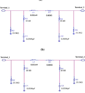
The SPICE model was imported to ADS environment to create a schematic diagram representing the TSV. The generated low-bandwidth circuit model which is symmetrical with respect to the TSV terminals is shown in Fig. 2.3
Though there are many components in Figure 2.3 to represent a simple TSV, which is just a small copper bar, each of them can be explained. We classify these components into two categories:
Components connecting TSV terminals
There are resistors and inductors in series R1 and L1 between the TSV input and output terminals. The presence of a small resistances, R1, is expected because of the high conductivity of copper used to implement the TSV. The impedance between the TSV terminals cannot be modeled by a small resistor alone. At high frequencies, the impedance of copper increases due to the skin effect [52], which reduces the effective cross section of the TSV contributing to the conduction of current. The impedance elevation caused by skin effect is modeled by an inductor, L1, in the TSV circuit model.
Components connecting TSV terminal and ground.
Figure 2.3. Low bandwidth lumped circuit model representing a fault free TSV
generated by HFSS 5MHz solution frequency from 3D full wave simulation results.
0.3nH
608MΩ
0.0006Ω
0.11nH 0.003Ω
1e-5Ω 1e-5Ω
0.018pF 0.018pF
19
The high resistors, R3 and R4, connecting each terminal to ground are due to the presence of dielectric between the TSV and the substrate which is connected to the ground. There are a pair of resistor and capacitor in series connection, R5 in series with C1 and R6 in series with C2, connecting each TSV terminal to ground. TSV metal at each port and the substrate can be considered as two conducting plates of a capacitor separated by the dielectric between them, which is by definition a capacitor. The small resistors R5 and R6 in series with the capacitors represent the resistance of the TSV metal from its terminals to the surface of the dielectric layer.
2.4 Analytical Verification
Here we only develop analytical approaches for a fault-free TSV.
A fault-free TSV can be modeled as a transmission line; we can develop the TSV’s analytical model with transmission line’s theory. Because the TSV is symmetrical, it can be represented by the transmission line model shown in Figure. 2.4.
In Figure 2.4, the voltage between port a and c, b and d is V(l, t),V(l+hTSV, t)
respectively. If we apply Kirchhoff’s voltage law, we get equation (2.4)
20
−𝑉(𝑙 + ℎ𝑇𝑆𝑉, 𝑡) − 𝑉(𝑙, 𝑡)
ℎ𝑇𝑆𝑉 = 𝜌𝑇𝑆𝑉 × 𝐼 (𝑙 + 1
2ℎ𝑇𝑆𝑉, 𝑡) + 𝐿𝑇𝑆𝑉 ×
𝜕𝐼 (𝑙 +12 ℎ𝑇𝑆𝑉, 𝑡)
𝜕𝑡 (2.4)
Equation (2.4), if ℎ𝑇𝑆𝑉 → 0, can be written as
−𝜕𝑉(𝑙, 𝑡)
𝜕𝑙 = 𝜌𝑇𝑆𝑉 × 𝐼(𝑙, 𝑡) + 𝐿𝑇𝑆𝑉×
𝜕𝐼(𝑙, 𝑡) 𝜕𝑡 (2.5)
after applying Kirchhoff’s current law, we can
−𝐼(𝑙 + ℎ𝑇𝑆𝑉, 𝑡) − 𝐼(𝑙, 𝑡) ℎ𝑇𝑆𝑉
= 𝐺𝑇𝑆𝑉× 𝑉 (𝑙 + 1
2ℎ𝑇𝑆𝑉, 𝑡) + 𝐶𝑇𝑆𝑉 ×
𝜕𝑉 (𝑙 +12 ℎ𝑇𝑆𝑉, 𝑡)
𝜕𝑡 (2.6)
From equation (2.6), if ℎ𝑇𝑆𝑉 → 0, we can write
−𝜕𝐼(𝑙, 𝑡)
𝜕𝑙 = 𝐺𝑇𝑆𝑉× 𝑉(𝑙, 𝑡) + 𝐶𝑇𝑆𝑉 ×
𝜕𝑉(𝑙, 𝑡) 𝜕𝑡 (2.7)
From equation (2.5) and (2.7), we can derive (2.8) and (2.9)
{
− 𝑑𝑉𝑠
𝑑ℎ𝑇𝑆𝑉 = (𝜌𝑇𝑆𝑉 + 𝑗𝑤𝐿𝑇𝑆𝑉)𝐼𝑠 (2.8)
− 𝑑𝐼𝑠
𝑑ℎ𝑇𝑆𝑉 = (𝐺𝑇𝑆𝑉+ 𝑗𝑤𝐶𝑇𝑆𝑉)𝑉𝑠 (2.9)
If we take the derivation of (2.8) and replace 𝑑𝐼𝑠
𝑑ℎ𝑇𝑆𝑉 from (2.9), we get (2.10)
−𝑑 2𝑉
𝑠
𝑑𝑙2 − 𝛾2𝑉𝑠 = 0 (2.10)
Solving equation (2.10), results in equation (2.11), (2.12).
{
𝛾 = √(𝜌𝑇𝑆𝑉+ 𝑗𝑤𝐿𝑇𝑆𝑉)(𝐺𝑇𝑆𝑉+ 𝑗𝑤𝐶𝑇𝑆𝑉) (2.11)
𝑍0 = √𝜌𝑇𝑆𝑉 + 𝑗𝑤𝐿𝑇𝑆𝑉
21
TSV resistances can be modeled with two components of AC resistance and DC resistance.
DC resistance is easy to calculate, the equation is given in (2.13)
𝑅𝐷𝐶_𝑇𝑆𝑉 = 𝜌𝑇𝑆𝑉× ℎ𝑇𝑆𝑉 𝜋 × (𝑑𝑇𝑆𝑉2 )2
(2.13)
In (2.13), 𝜌𝑇𝑆𝑉 = 1.724 × 10⁻⁸𝛺. 𝑚, ℎ
𝑇𝑆𝑉 = 50𝜇𝑚, 𝑑𝑇𝑆𝑉 = 5𝜇𝑚.
If we take these three values into equation (2.13), then we can get the DC resistance of the TSV, which is 0.043 𝛺. It has to be noted that the extracted resistance by CAD tools takes both the AC resistance and the DC resistance to extract the circuit models.
The skin depth of TSV, 𝛿𝑇𝑆𝑉 can be calculated with equation (2.14) [53]
𝛿𝑇𝑆𝑉 = √ 2𝜌𝑇𝑆𝑉 𝜔𝜇𝑇𝑆𝑉
× √√1 + (𝜔𝜌𝑇𝑆𝑉𝜀0)2+ 𝜔𝜌𝑇𝑆𝑉𝜀0 (2.14)
The skin depth for the TSV at 1GHz operation frequency is 2.09 𝜇𝑚.
𝑅𝐴𝐶𝑇𝑆𝑉 = 𝜌𝑇𝑆𝑉 × ℎ𝑇𝑆𝑉
𝜋 × (𝑑𝑇𝑆𝑉 × 𝛿𝑇𝑆𝑉′− (𝛿𝑇𝑆𝑉′)2) × (1 + 𝑌)
Where 𝛿𝑇𝑆𝑉′ = 𝛿𝑇𝑆𝑉(1 − 𝑒2×𝛿𝑇𝑆𝑉−𝑑𝑇𝑆𝑉)
22
For the cylindrical capacitance, we have equation 2.15 to calculate the capacitance
C = 2𝜋εℎ𝑇𝑆𝑉 ln (𝑏𝑎)
(2.15)
Where "a" represents the radius of the TSV and "b" is equal to the inner thickness of the substrate. Taking all this information into consideration, we get the capacitance is equal to 0.0594pF, which has a small variation with the results given by the CAD tool.
2.5Summary
This chapter presents the implemented 3D TSV structure in HFSS environment for 3D full wave analysis. The equivalent circuit models are extracted from the S-parameters, and imported to ADS environment for further circuit analysis. Analytical explanations for the structure and parameters of the TSV’s equivalent circuit are also given in this chapter. The mathematical model is developed with transmission line theory. The components in the TSV circuit models meet the analytical expectations.
Figure.2.5 Cylindrical capacitor between TSV conducting body and
23
Chapter 3
Effects of Faults on TSV Model Parameters
As mentioned in Chapter 1, there are typical defects such as pin-holes, voids and open circuits. We will study these defects in this chapter. In the real world, pin-holes or voids or opens cannot be added manually to TSVs, we cannot control the position of the pin-holes or voids, the size of the pin-pin-holes or voids, or other key parameters to analyze those faults. While with HFSS, we can easily deal with these kinds of faults. For example, to create a void fault, we can simply extract a small part of the inner side of the TSV body; to create a pin-hole fault, we can break the dielectric around the TSV body; to create an open fault, we can cut off the TSV body. Taking these advantages into consideration, we can study different types of faults to develop a solid model for TSV.
3.1 Effects of Pin-holes
3.1.1 Electric field distribution of a TSV with a pin-hole
For pin-holes, we expect a much higher leakage current compared with a fault-free TSV. In the fault free TSV model, the TSV body is surrounded by a dielectric, which is usually made of silicon dioxide. As a result, the path from TSV body to ground is open. In this case, we have a very small leakage current because of the high resistance from TSV terminals to ground. While for a TSV with a pinhole, there is a path from the TSV body to ground, which connects TSV to the substrate directly.
A pin-hole with dimensions of 2µm×2µm was created to see its effects on the electric field distribution. 3D simulations were performed under the same conditions as fault free TSV.
24
3.1.2 Equivalent circuit of a TSV with a pin-hole
We can calculate the resistance from TSV terminals to ground from equations 3.1 and 3.2. For a fault free TSV,
𝑅𝑇𝑒𝑟𝑚𝑖𝑛𝑎𝑙 𝑡𝑜 𝑔𝑟𝑜𝑢𝑛𝑑 = 𝑅𝑐𝑜𝑝𝑝𝑒𝑟+ 𝑅𝑑𝑖𝑒𝑙𝑒𝑐𝑡𝑟𝑖𝑐+ 𝑅𝑠𝑢𝑏𝑠𝑡𝑟𝑎𝑡𝑒 (3.1)
For a TSV with a pinhole,
𝑅𝑇𝑒𝑟𝑚𝑖𝑛𝑎𝑙 𝑡𝑜 𝑔𝑟𝑜𝑢𝑛𝑑 = 𝑅𝑐𝑜𝑝𝑝𝑒𝑟+ 𝑅𝑠𝑢𝑏𝑠𝑡𝑟𝑎𝑡𝑒 (3.2)
Figure 3.2 (a) and (b) show the resistance from TSV terminals to ground for a fault-free TSV and a TSV with a pinhole, respectively.
Figure 3.1. The effect of a pin-hole with dimensions of 2µm×2µm on the
25
For a TSV with a pin-hole, resistance of the dielectric is neglected because the pin-hole punches through the dielectric, connecting the TSV body to the substrate directly. The resistance of the dielectric is much greater than the resistance of the substrate and thus a significant fall in the resistance from TSV terminals to ground is expected.
The schematic diagram of the extracted circuit model remains almost unchanged, shown in Figure 3.3. The impedances between TSV terminals and ground, R3 and R6 in Figure. 2.3, fall sharply from 208MΩ to about 23kΩ.
(a)
(b)
Figure 3.2. Resistance from TSV terminals to ground (a) Fault-free TSV, (b)
26
We noticed that there is a minor difference between the impedance connecting the TSV terminals of faulty and fault free TSVs. This is an acceptable result as pin-holes in general are not in the electrical path between TSV terminals. Thus, they are not expected
to affect the impedance connecting TSV terminals in the circuit model.
Figure 3.3. The equivalent circuit of a pin-hole with dimensions of 2µm×2µm
on the electric field intensity in a resistive substrate.
27
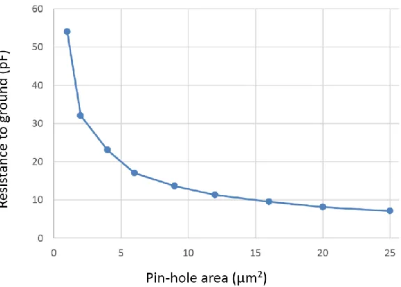
The overall TSV capacitance does not change significantly; the variation is only up to 14.3%. This can be understood if the nature of the TSV capacitance is taken into consideration. A cylindrical capacitor is formed between the TSV surface and the surrounding substrate that can be considered as two plates of a capacitor separated by silicon dioxide as an insulator. The pin-hole adds a resistor between the plates of TSV capacitors. If the added resistance becomes comparable with the AC resistance of the TSV capacitor, the TSV capacitance in the model will change as reported in section 4 where the effect of highly conductive substrate on the TSV model is characterized. Figure 3.4 shows the variations of capacitance to ground for different pin-hole sizes. Variations can be calculated by equation 3.1. For the case of a resistive substrate with low conductivity of 10 Siemens per meter, the variations in TSV capacitance due to the pin-hole are negligible.
Variation = 𝐶𝑓𝑎𝑢𝑙𝑡𝑦− 𝐶𝑓𝑎𝑢𝑙𝑡−𝑓𝑟𝑒𝑒
𝐶𝑓𝑎𝑢𝑙𝑡−𝑓𝑟𝑒𝑒 × 100% (3.1)
28
It can be seen that the resistance of the TSV terminals to the ground, R3 and R6, decreases when the pin-hole size increases. However, the relationship between resistance to ground and pin-hole size is not linear. For instance, when the size of a pin-hole increases by a factor of 2 from 1µm2 to 2µm2, R3 and R6 fall from 54kΩ to 32kΩ which
is less than a twofold drop. The inductors, L3 and L4, in the path of TSV terminals to ground in Figure. 3.5 are also dependent on the size of pin-hole, and as the size of the pin-hole increases, they decrease with the same variation rate of R3 and R4. The impedance composed of R1 and L1 connecting the TSV terminals remains nearly constant.
3.1.3 Effects on pin-hole positions
The above results have been obtained for a pin-hole right at the middle of the TSV. We may wonder whether the positions of the pin-holes can also affect the parameters of the equivalent circuit. As a result, the effects of different pin-hole locations on the extracted circuit model have also been determined through simulations.
Figure 3.5. Variations of the resistance of TSV terminals to ground in the
equivalent circuit with different pin-holes for a resistive substrate with 10 Siemens
29
Two pinhole are created near the top and the bottom of the TSV, respectively, shown in Figure 3.6. The equivalent circuit of these two cases are shown in Figure 3.7.
(a) (b)
Figure 3.6. (a)Pin-hole near the top. (b) Pin-hole near the bottom.
30
The results indicate that the overall effect of pin-hole location on the circuit model parameters is negligible. When the pin-hole is chosen to be very close to a TSV terminal, variations of the equivalent circuit parameters are less than 0.1%.
3.1.4 Effects on multi-pin-holes
The effects of multi-pin-holes have also been studied. The results indicate that the total area of the pin-holes determines the circuit parameters of the TSV model and the number of pin-holes, or their distributions over the TSV do not have a noticeable effect.
(a)
(b)
Figure 3.7. Equivalent circuit for TSV with a Pin-hole. (a) Near the top. (b)
31
3.2 Effects of Voids
3.2.1 Equivalent circuit for a TSV with a pin-hole
In a TSV with a void, we expect an increase in the resistance connecting both terminals of the TSV because part of the TSV conducting body is not formed, thus reducing the effective TSV cross section. Figure 3.8 shows the extracted circuit for TSV with a void, the cross section of which is 3µm in diameter, extending 3µm from the TSV surface toward the TSV body.
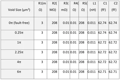
The extracted circuit model at 1GHz solution frequency shows that the equivalent circuit is the same circuit as in Figure 2.3 with almost the same parameter values. The presence of a void neither affects the TSV capacitance nor its resistance. We created voids of different sizes inside the TSV to see if there are any changes in the parameters of the equivalent circuit. Table 3.1 shows the variations of the parameters in the equivalent of different cylindrical shaped void sizes.
Figure 3.8. Equivalent circuit for TSV with a void (cross section 3µm diameter
extending 3µm from the TSV surface toward the TSV body).
32
The created voids are at the middle of the TSV. The height of all cylindrical shaped voids is 1µm, with different radius ranging from 0.5µm to 2.45µm.
From Table 3.1 we can see that parameters of the equivalent circuit remain almost the same. The simulation results indicate that even a larger void of cylinder shape with 4.9µm diameter within a TSV of 5µm does not have a noticeable effect on the equivalent circuit parameters.
This seems against intuition as a void takes a portion of TSV body and is expected to have an effect on the circuit parameters, such as increasing the resistances between the TSV’s terminals (R1 and L1). This result can be understood if the tendency of AC currents to be distributed over the surface of conductors is taken into consideration. At 1GHz solution frequency, where simulations have been conducted, the inner portion of the TSV does not play an important role as most of the charge carriers find their way through the surface of the TSV to flow from one TSV terminal to the other.
Table 3.1.Variations of TSV equivalent circuit parameters with different voids for
a substrate with 10 Siemens per meter conductivity.
Void Size (µm3)
R1(m Ω) R2( MΩ) R3( mΩ) R4( Ω) R5( Ω) L1 (nH) C1 (fF) C2 (fF)
0π (fault-free) 3 208 0.01 0.01 208 0.011 62.74 62.74
0.25π 3 208 0.01 0.01 208 0.011 62.74 62.74
1π 3 208 0.01 0.01 208 0.011 62.72 62.72
2.25π 3 208 0.01 0.01 208 0.011 62.72 62.72
4π 3 208 0.01 0.01 208 0.011 62.72 62.72
33
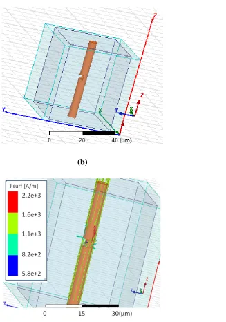
3.2.2 Current density distribution of a TSV with a void
Figure. 3.9(a) shows a TSV with a cylindrical void with cross-section of 3µm diameter
extending 3µm from the TSV surface toward the TSV body.
(a)
(b)
Figure 3.9. (a) TSV with a cylindrical void of 3µm diameter and 3µm height. (b)
34
It can be observed that the surface current density changes right after the void but it rapidly returns back to its nominal value. The void is just like a big obstacle at the center of a flowing river and the current is like the water flow, although the direction or performance of the water flowing near the obstacle will be abnormal, the general flow is mostly unchanged.
As a result, presence of voids in a TSV can be considered as a reliability issue which undermines its physical integrity. The electrical performance of TSV at high frequencies is not notably affected by voids unless they become large enough to reduce the overall AC current passing through the TSV.
3.2.3 Effects on multi-voids
The effects of multi-voids have also been studied. We created multi-voids as shown in Figure 3.10.
(a) (b)
Figure 3.10. (a) TSV with cylindrical multi-voids. (b) TSV with one cylindrical
35
In Figure 3.10 (a), we have a TSV with three cylindrical voids in series. In Figure 3.10 (b), we have one cylindrical void with the same volume. The results indicate that the total volume of the voids, the number of voids or their distributions over the TSV do not have a considerable effect on the electric performance.
3.3 Effects of Opens
3.3.1 Equivalent circuit for a TSV with an open fault
The TSV in Figure 3.11.is cut right at the middle, the gap between the two plates is 1µm.
The equivalent circuit of a TSV with an open fault is shown in Figure 3.12. It can be seen from Figure 3.12 that the small resistance and inductance connecting TSV terminals are replaced by small capacitances.
36
From Figure 3.12, we note that the capacitors connecting TSV terminals to ground, C3 and C4, is almost half that of a fault-free TSV.
We expect that as the open length increases, the capacitances decrease. Because the equivalent circuit is symmetrical, we can just take one capacitor into consideration, Table 3.2 shows the capacitance (C3) connecting TSV terminals with different open lengths.
A TSV with an open fault can be treated as two-plate capacitors, when the distance between the plates increases, the capacitance will decrease.
Figure 3.12. Equivalent circuit for a TSV with an open fault
37
3.3.2 Current density distribution of a TSV with an open fault
Figure 3.13 shows the current density distribution of a TSV with an open fault.
It is clearly shown that since the TSV is cut off and there is no current flowing from one terminal to the other.
Figure 3.13. Current density distribution of a TSV with an open fault Table 3.2. Capacitances connecting TSV terminals with different open lengths
Open Lengths (µm) 1 2 3 4 5
38
3.4Summary
39
Chapter 4
Substrate Effects on TSV Model Parameters
4.1 Equivalent circuit of a fault-free TSV in a highly conductive substrate
The resistivity of the substrate has a considerable effect on TSV model parameters. For instance, if a highly conductive epi-substrate with resistivity of 1mΩ.cm or conductivity of 100,000 Siemens per meter is used, the resistances from TSV terminals to ground fall significantly. The circuit model of a 50µm long TSV with 5µm diameter within a highly conductive substrate is shown in Fig 4.1
As compared to the circuit model for resistive substrate in Fig. 2.3, all component values remain unchanged other than R2 and R5 which fall from 208MΩ to less than 3.2MΩ. We can calculate the resistance from TSV terminals to ground:
𝑅𝑇𝑒𝑟𝑚𝑖𝑛𝑎𝑙 𝑡𝑜 𝑔𝑟𝑜𝑢𝑛𝑑 = 𝑅𝑐𝑜𝑝𝑝𝑒𝑟+ 𝑅𝑑𝑖𝑒𝑙𝑒𝑐𝑡𝑟𝑖𝑐+ 𝑅𝑠𝑢𝑏𝑠𝑡𝑟𝑎𝑡𝑒 (3.1)
Figure 4.1. TSV equivalent circuit models for a TSV within a highly conductive
40
In the case of TSV in a resistive substrate, 𝑅𝑠𝑢𝑏𝑠𝑡𝑟𝑎𝑡𝑒 contributes the most to the
resistance to ground. The bulk conductivity increases from 10 Siemens per meter to 105 Siemens per meter. As a result, the resistance to ground will be dramatically reduced.
4.2 Analysis of a TSV with pin-holes in a highly conductive substrate
4.2.1 Current density distribution
Figure 4.2(a) shows the current density distribution for a faulty TSV within a highly conductive substrate with 1µm2 pin-hole.
It can be observed that most of the current flows from one terminal, through the pin-hole, and then into the substrate in many directions. There is very limited current flowing to the other terminal after passing the pin-hole in a highly conductive substrate. This is because the substrate bulk conductivity is relatively high, which is close to the range of conductor. We may expect when the pin-hole size is large enough, there will be no connections between both terminals because in that case, the current will flow throughout the pin-hole totally.
Figure 4.2(a). Current density distribution for a faulty TSV within a highly
41
For the low conductivity case, Figure 4.2(b) shows the current density distribution for a faulty TSV within a resistive substrate with 1µm2 pin-hole.
It can be observed that although the current density decreases after the current passed the pin-hole, there are no considerable changes in the current flow in general. There are some leakage currents after the pin-hole is created, but it is not high enough to create component changes in the equivalent circuit model.
4.2.2 Equivalent Circuit
A pin-hole of 1µm² on TSV within a resistive substrate reduces the resistances of TSV terminals to ground from 208MΩ to 23.6KΩ as shown in Figure. 3.3. All other components in the TSV extracted model remain unaffected.
A pin-hole with the size of 1µm² on the same TSV within a highly conductive substrate (105 Siemens per meter) is also created. The equivalent circuit model is shown in Figure
4.3.
Figure 4.2(b). Current density distribution for a faulty TSV within a resistive
42
We find that there are two main difference between these cases. One is that the pin-hole itself reduces the resistances of the paths to ground to less than 6Ω. The other is that the pin-hole changes the components of the TSV equivalent circuit model. It can be seen that the large resistors between TSV terminals and ground, R2 and R5 in Figure. 3.3, have been replaced with relatively small resistors in series with inductors. The resistors are attributed to the low impedance path opened from TSV terminals to ground through the pin-hole and the inductors indicate that the impedances of the paths to ground increase with frequency.
Figure 4.3. TSV equivalent circuit models for a TSV within a highly
43
We may notice that the extracted circuit model does not include any capacitor since the pin-hole punched through the insulator and connected the plates of the capacitors formed between the TSV and the substrate. In this case, contrary to the case of high resistivity substrate, the current from TSV to ground is dominated by the conduction current through the low resistive paths from TSV terminals to ground.
The displacement current through the capacitors formed between the TSV and the substrate become negligible as compared to the conduction current. Thus the capacitors is omitted from the circuit model. Variations of TSV equivalent circuit components for highly conductive substrate with different size pin-holes are shown in table 4.1.
Figure 4.4. Impedances for a TSV within a highly conductive substrate with a
44
It can be seen that the impedance between the TSV terminals, R1 and L1, is constant while both the resistance and the inductance of each TSV terminal to ground experience a considerable reduction when the size of pin-hole increases.
When the pin-hole size reaches 12 µm², R1 and L1 both become infinity, which means that under this condition there is no connection between both terminals. When the pin-hole size reaches 12µm², the current generated from one TSV’s terminal will mainly flow into the substrate.
4.3 Analysis of a TSV with voids in a highly conductive substrate
4.3.1 Current density and electric field distribution
Figure 4.5 shows the current density and electric field distribution for a faulty TSV within a highly conductive substrate with 37µm3 void.
Table 4.1.Variations of TSV equivalent circuit parameters with different
pin-holes for a substrate with 105 Siemens per meter conductivity.
Pin-hole
Size (µm²) R1(mΩ) L1 (nH) R2(Ω) L2 (nH) R3(Ω) L3 (nH)
1 3 0.011 5.47 0.038 5.47 0.039
2 3 0.011 3.32 0.038 3.32 0.040
4 3 0.011 2.29 0.037 2.29 0.040
6 3 0.011 1.76 0.036 1.76 0.040
9 3 0.011 1.4 0.036 1.4 0.040
45
From current density distribution, we note that some fluctuations of the current flow occur near the void, but the main flow in general is smooth, there are almost no changes
(a)
(b)
Figure 4.5. (a) Current density distribution. (b) Electric field distribution for a
46
of current distribution for this case as compared to the case that TSV in a resistive substrate.
For electric field distribution, although there is a small field intensity change near the void, the field is more or less uniformly distributed. We can expect that the equivalent circuit for this case will not have a significant change.
4.3.2 Equivalent circuit
The structure and parameters of the equivalent circuit remain almost the same as compared to Figure 4.1.
4.4 Analysis of a TSV with opens in a highly conductive substrate
Figure 4.6 shows the current density distribution for a TSV within a highly conductive substrate with an open fault.
Figure 4.6. Current density distribution for a TSV within a highly conductive
47
We note that as compared to the open TSV in a resistive substrate, the current density of the surface is reduced to 10%, but the current density distribution remains with almost no changes.
4.5 Summary
In this chapter we studied the effects of different bulk conductivity of the substrate on the equivalent circuit models and their parameters.
48
Chapter 5
TSV with Bumps and Layers
5.1 Fault-free TSV structure
Based on the discussions in Chapter 2, we have implemented a TSV structure shown in Figure. 2.1. This structure only includes the TSV body, the dielectric layer and the substrate, while a complete TSV includes a passivation layer, bumps on the top and bottom of the TSV, a metal layer, a keep out zone and an active layer. For an accurate analysis, we have implemented a complete TSV structure as shown in Figure 5.1. The length, width and height of the bumps are 20µm, 20µm and 5µm, respectively. The thickness of the dielectric is 0.5µm.
49
5.2 Analysis of the complete fault-free TSV structure
5.2.1 Electric field and current density distribution
The TSV was excited with one voltage at its port to extract S-parameters. The frequency is swept from 1MHz to 1GHz, with the step size of 1MHz, and the solution frequency is set to 1GHz.
The top tin bump is assigned as terminal_1 and the bottom tin bump as terminal_2. Figure 5.2 (a) shows the electric field distribution and Figure 5.2(b) shows the current density distribution of the fault-free TSV. The electric field and the current density are uniformly distributed over the surface of the TSV and there is no current flowing into the substrate.
(a) (b)
Figure 5.2 (a) Electric field distribution of a complete TSV structure
(b) Current density distribution of a complete TSV structure
2.0e+6 1.7e+6 1.5e+6 E Field[V/m]
0 25 50(µm)
3.1e+3
9.3e+2
2.8e+2
8.2e+1
2.4e+1
7.2e+0 J surf [A/m]
50
5.2.2. Equivalent circuit and S-parameters
Figure 5.3 shows lumped circuit model representing the complete fault free TSV generated by HFSS from 3D full wave simulation at 1GHz solution frequency.
As compared to Figure 2.3, there are no significant changes, only the capacitors to ground, C1 and C2, increase from 0.0627pF to 0.079pF. The contact area of the dielectric and the conducting plates are larger, which will increase the capacitance.
Figure 5.4 shows the S-parameters of the TSV. S11 shows a minor return loss at 1GHz solution frequency and likewise, S21 indicates an insertion loss at high frequencies. These results are similar to what we got in Chapter Two.
Figure. 5.3. Lumped circuit model representing a fault free TSV generated by
HFSS from 3D full wave simulation at 1GHz solution frequency.
0.49nH
220MΩ
0.003Ω
0.16nH 0.016Ω
1e-5Ω 1e-5Ω
0.079pF 0.079pF
51
5.3 Analysis of the complete TSV structure with a pin-hole
5.3.1 Electric field and current density distribution
A pin-hole with the size of 2µm by 2µm was created on the silicon dioxide to see the electric field and current density distribution under this case. Figure 5.5(a) shows the electric field distribution and Figure 5.5(b) shows the substrate volume current intensity. The electric field intensity is higher near the pin-hole in the substrate because the dielectric separating the two conductors is broken. The current density of this fault model is also higher than the fault-free model because of the electric path from the pin-hole to ground which will result in greater leakage current.
(a)
(b)
Figure. 5.4. S-parameters of the fault-free TSV with ultimate structure.
(a) S11 and (b) S21
0.00 0.20 0.40 0.60 0.80 1.00
Freq [GHz] -75.00 -62.50 -50.00 -37.50 d B (S (1 ,1 )) HFSSDesign1
XY Plot 1
Curve Inf o
dB(S(1,1))
0.00 0.20 0.40 0.60 0.80 1.00 Freq [GHz] -0.04 -0.03 -0.02 -0.01 0.00 d B (S (2 ,1 )) HFSSDesign1
XY Plot 2
Curve Info
52
5.3.2 Equivalent circuit and S-parameters
Figure 5.6 shows lumped circuit model representing a faulty TSV with a pin-hole size of 2µm×2µm ultimate structure generated by HFSS from 3D full wave simulation at 1GHz solution frequency. As expected, most of the parameters keep no changes except the resistance to ground, say, R3 and R6, drop from 220MΩ to less than 23KΩ. This results are consistent with the results shown in chapter 3.
Figure. 5.6. Lumped circuit model representing a faulty TSV with a pin-hole
size of 2µm×2µm. (a) (b)
Figure. 5.5. (a) Electric field distribution. (b) Substrate volume current
intensity for a TSV with a pin-hole size of 2µm by 2µm
0.49nH
22.8KΩ
0.003Ω
0.16nH 0.016Ω
1e-5Ω 1e-5Ω
0.076pF 0.076pF
22.8KΩ
0 25 50(µm) 1.8e+7
1.4e+7 9.4e+6 4.7e+6 1.9e+1
53
Figure 5.7 shows the S-parameters of the TSV with a pin-hole of 2µm×2µm. As compared with Figure 5.4, both return loss and insertion loss have noteworthy changes, e.g., the maximum return loss decreases from -75dB to -55dB and the insertion loss increases from -0.04dB at 1GHz to -0.05dB at 1GHz.
5.3.3 Effect of pin-hole sizes on equivalent circuit
Table 5.1 shows the parameters of the equivalent circuit with different pin-hole sizes. If we recall the discussions in Chapter Three, the variations of parameters other than the resistance from TSV terminals to ground retain almost no changes. We have the same situation here. We note that the resistance to ground, R3 and R6, fall from 220MΩ to 55KΩ immediately after a pin-hole of 1µm by 1µm is created. R3 and R6 is decreasing when the pin-hole size is increasing, but the relationship is not linear. For example, when
(a)
(b)
Figure. 5.7. S-Parameters for a TSV with Pinhole of 2µm×2µm. (a) S11. (b)
S21.
0.00 0.20 0.40 0.60 0.80 1.00
Freq [GHz] -55.00 -50.00 -45.00 -40.00 d B(S (1 ,1 )) HFSSDesign1
XY Plot 1
Curve Info
dB(S(1,1)) Setup1 : Sweep
0.00 0.20 0.40 0.60 0.80 1.00
Freq [GHz] -0.050 -0.040 -0.030 -0.020 d B( S( 2 ,1 )) HFSSDesign1
XY Plot 2
Curve Info
54
the pin-hole size is 2µm×2µm, 4 times greater than 1µm×1µm, R3 and R6 fall from 55KΩ to 23KΩ, which is not 4 times smaller.
5.4 Analysis of the complete TSV structure with a void
Figure 5.8 shows TSV with a cylindrical void of 3µm diameter and 3µm height. The experimental results are almost the same as shown in Chapter Three, with no significant changes on the equivalent circuit’s parameter, the S-parameters, the electric field distribution and the current density distribution. As a result, although a void affects the TSV’s physical integrity, it does not have a noticeable effect on the electric performance of the TSV at high frequencies unless the void becomes large enough to either cut off the TSV or severely limit the current flow
TABLE 5.1
Variations of TSV equivalent circuit parameters with different pin-holes for a
substrate with 10 Siemens per meter conductivity.
Pin-hole Size
(µm²) R1(Ω) R2(Ω) R3(KΩ) R4(Ω) R5(Ω) R6(KΩ) L1 (nH) L2 (nH) C1 (pF) C2(pF)
1 0.016 0.003 55 1E-5 1E-5 55 0.164 0.488 0.078 0.078
2 0.016 0.003 33 1E-5 1E-5 33 0.164 0.488 0.077 0.077
4 0.016 0.003 23 1E-5 1E-5 23 0.164 0.488 0.076 0.076
6 0.016 0.003 17 1E-5 1E-5 17 0.164 0.488 0.076 0.076
9 0.016 0.003 14 1E-5 1E-5 14 0.164 0.488 0.074 0.074
12 0.016 0.003 11 1E-5 1E-5 11 0.164 0.488 0.074 0.074
16 0.016 0.003 9.5 1E-5 1E-5 9.5 0.164 0.488 0.073 0.073
20 0.016 0.003 8.2 1E-5 1E-5 8.2 0.164 0.488 0.072 0.072
55
(a)
(b)
Figure. 5.8. (a) TSV with a cylindrical void of 3µm diameter and 3µm height. (b)
Surface current density distribution at 1GHz solution frequency.
0 20 40(µm)
3.2e+3
9.1e+2
2.6e+2
7.2e+1
2.0e+1
5.7e+0 J surf[a/m]
![Figure 1.1 Microprocessor Transistor Counts from 1971 – 2011 [56]](https://thumb-us.123doks.com/thumbv2/123dok_us/1408966.1173495/21.612.159.538.122.431/figure-microprocessor-transistor-counts-from.webp)
![Figure. 1.2 Three-dimensional IC [14]](https://thumb-us.123doks.com/thumbv2/123dok_us/1408966.1173495/22.612.227.416.228.483/figure-three-dimensional-ic.webp)
![Figure 1.5 [20] shows the fabrication process for three-dimensional ICs.](https://thumb-us.123doks.com/thumbv2/123dok_us/1408966.1173495/24.612.144.532.219.457/figure-shows-fabrication-process-dimensional-ics.webp)
![Figure. 1.8 Damages on TSV after probe touchdown [20]](https://thumb-us.123doks.com/thumbv2/123dok_us/1408966.1173495/28.612.220.419.74.262/figure-damages-on-tsv-after-probe-touchdown.webp)