167 | P a g e
DESIGN OF INTER INTEGRATED CIRCUIT WITH
HIGH PERFORMANCE WISHBONE CONTROLLER
Raja Krishna Motupalli
1, L. Srinivas Reddy
2 1M. Tech (DECS) Scholar,
2Asst. Professor (DECS)
Nalanda Institute of Engg& Tech. (NIET), Siddharth Nagar, Guntur, A.P, (India)
ABSTRACT
This article gives the designing of serial data communication using I2C master bus controller. I2C stands for Inter-integrated circuit. This I2C master needs a slave; hence we are going to interface it with MAXIM DS1307. I2C initiates the data transmission instructions and the slave has to respond for it. The I2C bus master is designed by using an efficient hardware description language i.e., Verilog HDL. This design has simulated and synthesized on XILINX ISE tool. It can be used to interface low speed peripherals say embedded system, mobile phones, motherboard, set top boxes, DVDs or other electronic devices are considerable.
Keywords:
Inter Integrated Circuit, Protocol, Bus
I.
INTRODUCTION
For serial data communication, we need to interface the peripherals using protocols. There are some protocols
which is for interface in between low speed and high speed peripherals. Some of these are 232, 422,
RS-485, SPI (Serial peripheral interface), Micro wire and etc. These protocols have need of more pin connection in
the IC(Integrated Circuit) intended for serial data communication, as the physical size of IC have reduced over
the years; we necessitate less amount of pin connection for serial data transfer.
USB/SPI/Micro wire and typically UARTS are all just one point to one point data transfer bus systems. They
employ multiplexing of the data path and forwarding of messages to examine various devices. To conquer this
problem, the I2C protocol was introduced by Phillips which has need of only two lines for communication with
two or more chips. It can be able to control a network of device chips. It uses just a two general purpose I/O pins
whereas; other bus protocols require more number of pins and signals to interface devices.
In this article, we are proposing the implementation of I2C bus protocol for interface in between low speed
peripheral devices. In controlling applications, this bus is the best one; where the related devices of the system
can added or removed from the system. It is also useful for communication purpose; the communication is in
between multiple circuit boards in equipments. Here we can use the bus with or without shielded cable; this is
depending on the transferring/receiving speed and the distance between transferring and receiving devices.
I2C bus plays a role as a medium intended for communication wherever the master controller can be used to
send and accept data to as well as from the slave i.e., DS1307. The low speed peripheral, consider the slave
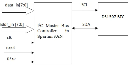
DS1307 is interfaced with I2C master bus and synthesized on Spartan 3AN. Fig 1 shows theI2C bus system
contains of the I2C master controller employed on a FPGA. In this implementation, the real time clock device
168 | P a g e
Fig 1: I/O Diagram of I2C Master Controller interfaced withDS1307 RTC slave deviceThe design of proposed system has explained in section II. It has designed by using Verilog HDL and
synthesized on Xilinx ISE tool.
II. PROPOSED SYSTEM
2.1 I
2C protocol
I2C is abbreviated as Inter Integrated Circuit. It is a two wire, bi-directional serial bus. It can able to provide
effective data communication between two devices. I2C bus can support many devices. It maintains unique ID
for every predictable device. In fig 1, we are giving the inputs of data_in and addr_in are each of 8 bits. To
initiate the bus controller we have given reset and clock signals. The R/ w signalis given as an input to the system. It is used to specify either master or slave act as a transmitter in the data communication.
Already we know that the physical I2C bus consists of just two wires. These are called SCL and SDA. SCL is
the clock line, can be used to coordinate all data transfers over the I2Cbus. SDA is a data line. Each and every
device which is on the I2C must be connected to the SCL line and SDA data line. These SCL and SDA lines are
"open drain" drivers they are pulled up via pull up resistors.
The I2C bus is at idle mode when both SCL and SDA areset to logic 1 level. The bus begins when the
master(controller) desires to send out data to a slave(DS1307)by providing a start sequence on the I2C bus,
which has high to low changeover on the SDA line at the same time the SCL line is high as shown in Fig2(a).
We can understand and considered that the bus is busy after the START condition.
Fig 2: (a) START sequence (b) STOP sequence
The master sends the slave address after the START condition. The slave device is to respond for the master
which has matched with the sent address. The response is made by an acknowledgement bit on the SDA line by
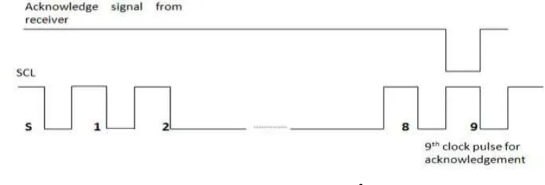
pulling it to low. Data has to transfer 8 bits in sequence and placed on the SDA line where MSB is the start bit.
The slave device sends an acknowledgement bit after every receiving of 8 bits. By this we have to know that
actually 9 SCL clock pulses will require for transferring of 8 bits data. Ti has shown in fig 3. The receiver
device sends a low acknowledgement bit when it receives the data and is ready to accept the data. It cannot
169 | P a g e
by sending STOP sequence. In above figures, 2(b) shows the STOP sequence, where the SDL line is low andSCL line is in high.
Fig 3: Acknowledgement on the I2C bus
2.2 Serial Data Communication
This I2C bus has two modes of operations. These are master transmission and master receiver. The I2Cmaster
bus can initiate the data transfer and can have the capability to drive both SDA and SCL lines. The slave device
(DS1307) is addressed by the master. The only work is that the sending data on SDA has issued by the slave
device.
In master transmission mode, the master sends a slave address after initiating the after theinitiation of the
START sequence. The address byte holds the 7bit DS1307 address, which is given by 1101000, has followed by
the direction bit .The device outputs acknowledge on the SDA line after the address byte has received
anddecoded. The master transmitsthe address of a register. It has to do this operation after the slave address +
write bit has acknowledgedby the DS1307. This address is going to set the register pointer on the DS1307. The
master stats the process of sending data and the slave will give the acknowledgement every time when it
receives the 8 bit data. To terminate the write operation, the master has to generate STOP condition.
Consider, the master receiver mode, the operation of handling the first byte is as same as the master
transmission mode. On the other hand, the transfer direction has reversed and this is indicated by the direction
bit. Serial data is transmitted through the slave i.e., DS1307 on the SDA at the same time as the serial clock is
input on SCL.
Fig 4: The Master Transmission Mode
170 | P a g e
START and STOP bits are beginning and ends of the master transmitter and receiver respectively. In this mode,after the generation of start condition by the master, the first bit received by the receiver is the address bit. The
address bit consists of 7 bits of slave address i.e., 1101000. It is followed by the direction bit. The device places
the acknowledgement on the SDA line when it completes the action of receiving as well as decoding of the
address byte. The slave i.e., DS1307 starts its operation of transmit data first with the register address, where the
register pointer has indicated. If the register pointer has not pointed before the beginning of a read mode, the
first address that is read considered as the last one stored in the registerpointer. The DS1307 must need to
receive a “notacknowledged” to stop a read operation.
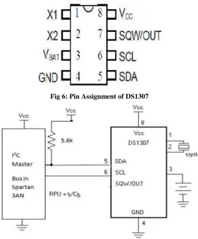
2.3 MAXIM DS1307
The DS1307 is a slave and it supports a bi-directional, two wire bus. It is used for data transmission followed by
a protocol initiated by the master.
Fig 6 gives you the clarification on pin placements of DS1307 and there another fig 7 shows the interface
connection of I2C.
Fig 6: Pin Assignment of DS1307
Fig 7: DS1307 Connected To Two Wire Data Bus
III. SOFTWARE IMPLEMENTATION
The I2C master controller design is made based on finite state machine (FSM) scheme and it is designed by
using one of the hardware description languages that is Verilog HDL. FSM is a sequential circuit and to store
the previous outputs and the output of the next state is going to depend on the present and past values. The
171 | P a g e
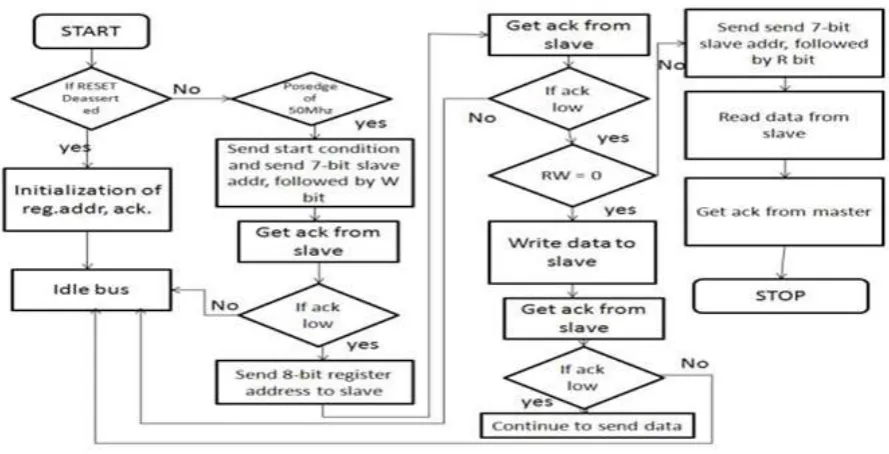
Algorithm
STATE 1: This is an idle condition. Here the I2C bus doesn’t able to perform any operation (in this mode SCL
and SDA are high).
STATE 2: This is start condition. Here the master initiates START for transmission of data (SCL remains high
and SDA varies from high to low).
STATE 3: This is a slave address- write condition. Here the master sends the slave address-write to the slave
i.e., 11010000.
STATE 4: The salve matched with the address which is sent by the master sends an acknowledgement for the
response to the master.
STATE 5: Here the register address of 8 bits transferred to the slave by the master and the slave gives the
response by sending the acknowledgement to the master.
STATE 6: Now the data has to transmit to the slave by the master. It sends the acknowledgement when it
receives the data.
STATE 7: It is a stop condition. Here, the slave sends a STOP bit to terminate the process of communication
(SCL will be high and SDA increases from low to high).
To perform the read operation, we need to do the write operation first and then after read operation will perform.
The slave address for read operation is given as 11010001. We don’t need to perform STATE 7 in read
operation.
STATE 8: The master sends slave address to the slave for performing the read operation.
STATE 9: Master receives the data from the slave and master gives acknowledgement to the slave.
STATE 10:To terminate the communication process, master sends a STOP bit (SCL will be high and SDA
deceases from Low tohigh).
The below fig 8 gives the flowchart I2C master bus communication with the slave.
172 | P a g e
IV.SIMULATION RESULTS
In this paper we are designing the I2c master controller which is used control the Slave. This is protocol which
is used to make communication between the devices and controller. The design is synthesised in Verilog HDL
173 | P a g e
V.CONCLUSION
This paper presents I2c master design which makes the communication between the devices. The controller is
master device which initiates the communication for slaves. This is designed with Verilog. This is synthesised
Xilinx ISE 13.2 i.
VI. REFERENCES
[1] Philips Semiconductor “I2C Bus Specification “version 2. 1, January 2000.
[2] Maxim integrated “DS1307 64 x 8, Serial, I2C RealTime Clock”, 2008.
[3] Prof. Jai Karan Singh “Design and Implementation ofI2c master controller on FPGA using VHDL,”
IJET,Vol 4 No 4 Aug-Sep 2012.
[4] Raj kamal,“Embedded system: Architecture programming and Design”, Tata McGraw Hill,2008.
[5] Stuart Sutherland, “Verilog® HDL Quick Reference Guide”, IEEE Std 1364-2001.
[6] Tim Wilmshurst, “Designing Embedded Systems with PIC Microcontrollers: Principles and Applications”
Elsevier Ltd publications, 2007.
[7] Xilinx “Spartan-3A/3AN FPGA Starter Kit Board User Guide, “version 1.1,2008.
[8] A. P. Godse, D.A.Godse, “Microprocessor, Microcontroller& Applications”Technicalpublications,2008.
[9] Vincent Himpe, “Mastering the I2C bus” Elektor Verlag publications, 2011.
[10] Pong P.Chu, “FPGA Prototyping by Verilog Examples:Xilinx Spartan – 3 Version” Wiley,2008.
[11] Mano, Ciletti, “Digital Design”Pearson Education India,edition 4,2008.
[12] M.Morris Mano, “Digital Design”, EBSCO publishing, Inc.,2002.
[13] Frank Vahid, “Digital Design with RTL Design,Verilog and VHDL”VP and Executive publisher,2010.
AUTHOR DETAILS
RAJA KRISHNA MOTUPALLI, pursuing his M.tech (DECS) from Nalanda
institute of Engineering and Technology(NIET),Siddharth Nagar, Kantepudi
village,Satenepallimandal, Guntur Dist., A.P, INDIA.His interest in
communication field and also in protocols which is used to transfer the data.
L. SRINIVAS REDDY has completed his M.tech and currently working as an
Asst.professor (DECS) from Nalanda institute of Engineering and Technology
(NIET), Siddharth Nagar, Kantepudi village,Satenepalli mandal, Guntur
Dist.,A.P, INDIA. His interest and excelled in digital design field. He has