International Journal in IT and Engineering
http://www.ijmr.net
43High-Voltage Switch Using Series-Connected IGBTs
With Simple Auxiliary Circuit
*Gaurav Trivedi
ABSTRACT
For high-voltage applications, the series operation of devices is necessary to handle high voltage
with limited voltage rating devices. In the case of self turn-off devices, however, the series
operation of devices is very difficult. The main problem associated with series-connected devices
is how to guarantee the voltage balance among the devices both at the static and the dynamic
transient states. This paper presents a simple and reliable voltage-balancing circuit for the series
operation of devices to overcome the disadvantages of solutions presented so far, such as
complex control or circuit, low reliability, and limited number of devices to be connected. The
proposed balancing circuit realizes a complete Voltage balancing at both static and dynamic
states and allows series operation of an almost unlimited number of devices. The operation
principle and analysis are presented and tested on 16 series connected insulated gate bipolar
transistors to handle 20-kV/400-A switching.
International Journal in IT and Engineering
http://www.ijmr.net
44 INTRODUCTIONPOWER semiconductor device technology has been continually developed far to get higher
voltage/current ratings, lower conduction/switching losses, and easier drive. As a result, the
performance of devices has been much improved and new devices such as insulated gate bipolar
transistors (IGBTs), integrated gate commutated thyristors (IGCTs), etc. have been presented.
Among various power devices, the IGBT is becoming the best candidate from low- to
high-power applications because it has advantages which include high voltage/current rating, fast
switching, and easy drive capabilities. The recently presented IGBT has a 6.5-kV/3-kA rating. In
recent years, the demand for high-voltage conversion applications, such as high-voltage
inverters, high-voltage pulse generators, high-voltage dc transmission systems (HVDC),flexible
ac transmission systems (FACTS), etc., have been increased. Since the voltage rating of these
applications usually ranges several tens of kilovolts, the power processing cannot be
accomplished with any single device. To do this, several devices should be connected in series
and operated simultaneously. For the self turn-off device, however, the series operation of
devices is very difficult because of tolerances in device characteristic and/or the mismatching of
the driving circuit. Recently, the series operation technique for power semiconductor devices,
especially IGBTs, has been introduced and discussed in [1]–[4]. One of the most important
aspects in series operation of devices is to equalize the static and dynamic balancing of the
voltage. The static voltage balancing can be simply achieved by connecting small balancing
resistors in parallel with each device. The dynamic voltage balancing during the switching
transient is much more difficult to achieve. Two dynamic voltage-balancing techniques are
available: load-side balancing and gate— side balancing. The load-side balancing employs a
snubber circuit and/or a clamp circuit. The snubber circuit and/or clamp circuit provide dynamic
voltage balancing by limiting the device voltage rising rate dv/dt and/or clamping the peak
voltage. This technique, however, cannot be used for high-power applications since much loss is
involved in the snubber and clamp circuits which is proportional to the switching frequency. To
solve this problem, an active gate control technique has been presented in the last few years,
International Journal in IT and Engineering
http://www.ijmr.net
45 Fig.1:Proposed auxiliary circuit for series operation of devices (inside dashed line )Fig. 2. Typical voltage waveforms of IGBTs during a switching transient
Each gate drive circuit should be actively controlled so that all device voltages are increased or
decreased at the same rate. To do this, each voltage of the devices has to be sensed and fed back
to the active gate control circuit, resulting in a complex drive circuit, low reliability, and
increased switching loss [6]. Therefore, this technique may not be an economical and practical
solution. In this paper, a new simple voltage-balancing circuit is presented for both the static and
dynamic voltage balancing as shown in Fig. 1. This circuit, which consists of two small
International Journal in IT and Engineering
http://www.ijmr.net
46 active gate control effect. Additional snubber circuits or a special complex gate drive are notrequired. In addition, the proposed scheme gives a minor effect on the switching time so that it
has much lower switching loss compared to the conventional active gate control technique.
Therefore, the proposed technique is simple, low in cost, with high reliability and an unlimited
number of devices to be connected in series.
( a ) ( b )
International Journal in IT and Engineering
http://www.ijmr.net
47 The operation principle and analysis are presented and tested on 16 series-connected IGBTs tohandle 20-kV/400-A switching. The experimental results with and without the proposed
auxiliary circuit are compared.
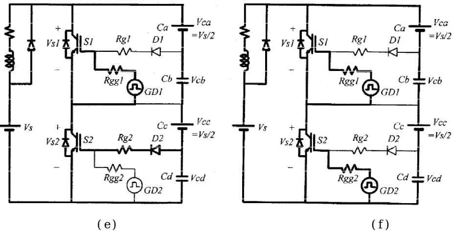
( e ) ( f )
Fig. 3. Operational modes. (a) Mode 1. (b) Mode 2. (c) Mode 3. (d) Mode 4. (e) Mode 5. (f) Mode 6.
II. SERIES OPERATION OF DEVICES:
The series operation of self turn-off devices is not easy because of the following reasons:
• unequal device switching characteristics;
• unequal device leakage current;
• unequal stray inductance in the series circuit;
• unequal gate drive delay.
Fig. 2 shows the typical waveforms of two series-connected IGBTs. After the gate signal goes
off, the device voltages are increased in different dv/dt rates and reach unbalanced peak and
steady state value. The difference of dv/dt and the peak mainly depend on the difference of
International Journal in IT and Engineering
http://www.ijmr.net
48 of steady-state voltage depends on the difference of the leakage current and the outputcapacitance of each device. If the peak voltage of one device goes higher than the device rating,
that device will be broken and the overall system will fail. Therefore, the voltage-balancing
technique is necessary to balance the device voltage, even when all bad conditions are
encountered.
A simple resistive voltage-dividing circuit guarantees the voltage balance of devices in the static
conditions. The dynamic balancing of devices, however, is much more difficult to achieve. Using
a snubber circuit for dynamic voltage balancing is not practical, since much loss should be
involved . The active gate control technique achieves dynamic voltage by device voltage
feedback . This, however, has a reliability problem and additional switching loss. The proposed
technique achieves dynamic voltage balance with a simple auxiliary circuit, which is a simple,
low-cost, and reliable technique.
III. OPERATION PRINCIPLE:
The proposed voltage-sharing circuit consists of two capacitors, three resistors, and one diode,
and all these components have a very small rating compared to those of the main switching
devices R1, R2 are voltage-sharing resistors, obviously for static voltage balancing. The other
components are for the dynamic voltage balancing. The operation of the static voltage balancing
is obvious and, thus, omitted here. The operational mode diagrams and waveforms of the
proposed circuit are shown in Figs. 3 and 4. To simplify operation of the dynamic voltage
balancing, voltage-dividing resistors are omitted and two series-connected IGBTs are considered.
It is assumed that Ca and Cc are charged with Vs/2and are much bigger (about ten times) than
Cb and Cd . Therefore, Ca and Cc are considered here as constant voltage sources, Vs/2 and the
switch S2 is turned on earlier and turned off later than S1 for any reason. GD1 and GD2 are basic
gate drive signals. The proposed circuit has six operating modes within each switching period.
Mode 1: S1 and S2 are turned on, the gate voltages of GD1 and GD2 are high. Because the
voltage of Ca and Cc is Vs/2 , the voltages of Cb and Cd are charged with – Vs/2 . Diodes Da
International Journal in IT and Engineering
http://www.ijmr.net
49 Mode 2: The gate drivers of S1 and S2 go off but the gate driver of S2 is off a little bit earlier.The switch current is decreasing gradually and, at the same time, the switch voltage of S2 starts
increasing first and that of S1 follows Cb and Cd are charged up from – Vs/2. The voltage of S2
is increased more rapidly than that of S1 and reaches the steady-state value Vs/2 first. The
voltage of Cd also reaches zero first.
Mode 3: Since the voltage of S1 is still lower than Vs/2, both voltages of S1 and S2 are
continually increased, and then the voltage of S2 is increased to more than Vs/2. At the same
time, the voltage of Cd goes positive, and this voltage is applied to the gate terminal of S2
through D2 and Rg2 resulting in slightly turning on of S2. Therefore, the rising voltage of S2 is
decreased sharply, and then the voltage of Cd is also decreased trying to turn off of S2 again. At
the end of this mode, the voltage of S1 reaches Vs/2 and then all switches are well balanced.
International Journal in IT and Engineering
http://www.ijmr.net
50 Fig. 5. Simulation circuitMode 4: The switch S1 and S2 are turned off with the balanced voltage Vs/2. Load current
freewheels through the diode.
Mode 5: Now, the gate driver of S1 is on first and that of S2 follows a little bit later. When S1
starts turning on, the overvoltage is applied to switch S2. Then, the voltage of Cd is increased to
positive as that of Mode 3, which turns on S2 slightly and reduces the voltage of S2. Both
voltages of S1 and S2 reach zero at the end of this mode.
Mode 6: Both switches are turned on completely. The Cb and Cd are charged to – Vs/2, again.
This is the end of one switching cycle. The dynamic voltage balancing is achieved at any
International Journal in IT and Engineering
http://www.ijmr.net
51 IV. FEATURES OF THE PROPOSED CONVERTER: A. Automatic Voltage BalancingThe static voltage balancing is simply achieved by the voltage-dividing resistors, as in the other
balancing techniques[1]–[5]. The dynamic voltage balancing is automatically achieved by the
action of the simple auxiliary circuit. The switch voltage fed back through - - ( –D2– ), which
slightly turns on the switch again, limiting the switch voltage with the normal voltage. This
action is just like the active voltage clamping. Therefore, the auxiliary circuit provides the
dynamic voltage balancing at any condition, including unequal device switching characteristics,
unequal stray inductance, unequal gate drive delay time, etc. Neither additional control circuit
nor special gate drive is necessary. There is no additional switching loss, either. The number of
devices to be connected is not limited
International Journal in IT and Engineering
http://www.ijmr.net
52 ( b )International Journal in IT and Engineering
http://www.ijmr.net
53 B. Simple and Low Loss:The auxiliary circuit consists of all passive components and all small power ratings compared to
the main devices. The loss involved with the auxiliary circuit is almost negligible. Therefore, the
proposed technique is a very efficient, reliable, and economic solution.
V. DESIGN CONSIDERATIONS:
A. Decision of Capacitors
To detect the overvoltage, the voltage of capacitor Ca ( Cc ) has to be almost constant during a
short switching period. Therefore, Ca ( Cc ) should be much bigger than capacitor Cb ( Cd ). The
empirical range of Ca ( Cc ) is about 100 nF. The Cb ( Cd ) is charged and discharged repeatedly
at every switching period. In order to get proper operation and to reduce loss, Cb ( Cd ) should
be much smaller, although it depends on the switching frequency. At several kilohertz switching
frequency range, 10% of Ca ( Cc ) is enough for Cb ( Cd ).
B. Design of Resistors
If the voltage-dividing resistors are too small, the static balancing is well achieved, but the loss is
increased. If the resistor are too big, the static balancing will fail. Therefore, the voltage-dividing
resistors should be designed by considering the leakage current of devices and loss. The gate
resistor Rg1 ( Rg2 ) should also be designed carefully. The device voltage is fed back to the gate
through Ca ( Cc ) and Rg1 ( Rg2 ), which provides the dynamic voltage balancing. The feedback
effect is not so sensitive with Rg1 ( Rg2 ) , but the dynamic voltage balancing is not properly
achieved if Rg1 ( Rg2 ) is too high or too low. (If Rg1 ( Rg2 ) is too high, the feedback effect is
reduced and so is the voltage balancing or vice versa.) The empirical range of Rg1 ( Rg2 ) is
International Journal in IT and Engineering
http://www.ijmr.net
54 C. DC-Link Voltage VariationCa ( Cc ) is constantly charged with the voltage of Vs/2 and Cb ( Cd ) is charged with – Vs/2 and
discharged to zero according to the switching state. If the dc-link voltage is increased, the
voltage of Ca ( Cc ) should be increased to allow proper operation. The main charging path of Ca
and Cb is the Rg and the gate-emitter junction during the turn-off state of switches. If the dc-link
voltage is increased abruptly, the voltage of Cb ( Cd ) can be positive and switches S1 and S2
can be turned on without the turn-on gate signal, resulting in undesirable operation. Therefore,
the dc-link voltage should not be changed abruptly. This effect, however, can normally be
ignored since the dc-link capacitance is usually very high and the voltage is changed very slowly.
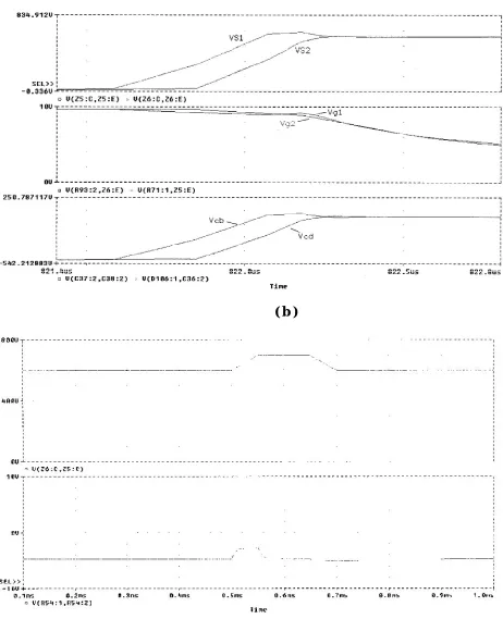
VI. SIMULATION RESULTS
To verify the operation of the proposed circuit, an example circuit, two series-connected IGBTs,
is designed as shown in Fig. 5 and simulated using PSPICE. To give an intentional difference in
switching conditions, the gating signal of S2 is delayed 0.2 us. Fig. 6 shows the simulated
waveforms during turn-on and turn-off transients. The feedback through auxiliary circuits is
shown in Fig. 6. During turn-on transient, the gating signal of S1 is applied first and the voltage
of S1 starts decreasing, as shown in Fig. 6(a). This means that the voltage of S2 is increasing
over the steady-state voltage Vs/2. This overvoltage charges Cd and applies a positive voltage to
the gate of S2 and, thus, S2 is turned on slightly, even though the real gating signal of S2 is not
yet applied. Therefore, the dynamic voltage balancing is achieved during the turn-on transient.
During the turn-off transient, S1 is turned off first and the voltage of S1 is increased and reaches
Vs/2 first. If Vs1 is increased over the steady-state voltage Vs/2, a positive voltage is applied to
the gate of S1 and the voltage of S1 is decreased and stays at Vs/2 until the voltage of S2 reaches
Vs/2, as shown in Fig. 6(b). Therefore, the dynamic voltage balancing is also achieved at the
International Journal in IT and Engineering
http://www.ijmr.net
55 Fig. 8. Experimental circuit diagram for series operation of 16 IGBTs.Fig. 9. Voltage and current waveforms of series-connected switches. Top:voltage (10 kV/div); bottom: current (200 A/div). Time (5 s/div).
Fig. 7 shows the simulated waveforms when the dc-link voltage is abruptly changed to see the
effect of dc-link voltage variation in the turn-off steady state. With a 100-V rise of dc-link
International Journal in IT and Engineering
http://www.ijmr.net
56 Therefore, the unwanted turn-on effect of IGBTs does not occurr, unless the dc-link voltage isnot changed too abruptly.
(a)
(b)
International Journal in IT and Engineering
http://www.ijmr.net
57 VII. EXPERIMENTAL RESULTSTo verify the operation of the proposed circuit, a 20-kV 400-A single-pole switching circuit has
been built and tested. Fig. 8 shows the experimental circuit diagram with the parts numbers of
the components used. Sixteen IGBT modules (1200 V/400 A, SKM400GB124D from Semikron)
are series connected with the proposed auxiliary circuit. As a loadR = 50ohms, and L= 100µH
are used. All gate drivers have the same characteristics except those of S1. S1 is turned on a little
bit later and turned off a little bit earlier than the others to give an intentional difference in
switching conditions.
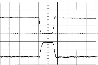
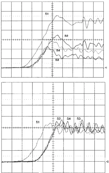
Fig. 9 shows the voltage and current waveforms of the switches connected in series. It can be
seen that the switching waveforms are clean. just like the waveforms of a single-switch circuit,
thanks to the voltage-balancing function of the proposed auxiliary circuit. Fig. 10 shows the
voltage waveforms of four interesting switches during the turn-off transient period with and
without the auxiliary circuit, and Fig. 11 shows the extended waveforms of Fig. 10. As shown in
Figs. 10(a) and 11(a), there exists a big imbalance among the switch voltages since the auxiliary
circuits are not included. The voltage of S1 is increased much higher than the others since S1 is
turned off early. In addition, the other voltages of the switches are not the same, either due to
small differences of characteristics and stray inductances among devices. The transient voltages
of switches when the auxiliary circuits are included are almost the same, even though S1 is
turned off early, thanks to the balancing action of the auxiliary circuit. The dynamic voltage
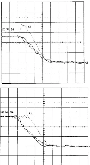
balancing is done well. Fig. 12 shows the voltage waveforms of switches during the turn-on
transient. When the auxiliary circuits are not included, there exists a high voltage peak across S1
since S1 is turned on later. When the auxiliary circuits are included, however, there is no voltage
peak, as shown in Fig. 12(b). The voltage imbalance of switches is less than 15% during the
turn-off transient and less than 5% during the turn-on transient. The dynamic voltage balancing is
performed well for both turn-on and turn-off transients since 20% of voltage imbalance is usually
International Journal in IT and Engineering
http://www.ijmr.net
58International Journal in IT and Engineering
http://www.ijmr.net
59 Fig. 12. Voltage waveforms of switches during turn-on transient. (a) WithoutauxiliaryInternational Journal in IT and Engineering
http://www.ijmr.net
60 Fig. 13. Photograph of the series-stacked IGBTs with gate drivers.VIII. CONCLUSION
A novel technique for series operation of IGBTs was presented. The operation, analysis, features,
and design considerations were illustrated and verified by the experimental results on a
20-kV/400-A prototype with 16 series-connected IGBTs. It has been shown that the dynamic
voltage balancing as well as the static balancing are well achieved with the proposed auxiliary
circuit. The proposed technique has many distinctive advantages over those previously
presented, as follows:
• simple and low cost;
• high reliability;
• extendibility (unlimited number);
• no additional loss.
These advantages make the proposed technique very promising for high-voltage high-power