Designing Fir Filter Using Modified Look up Table Multiplier
T. Ranjith Kumar
Scholar, M-Tech (VLSI) GITAM University, Visakhapatnam Email id:[email protected]
ABSTRACT- With the advancement in device scaling, semiconductor have met the cost, speed and power performance. In addition to that, the projections of the international technology roadmap for semiconductors, the total system on chips content exceeds by 90% in the embedded memories. Besides this, the memory-based computing structures are relatively regular than the multiply–accumulate structures and offer advantages like, greater potential for high-throughput, low-latency implementation and less dynamic power consumption and thus finds its application in DSP processors. Distributed arithmetic (DA)-based computation is widely used because it can be implemented efficiently on memory-based circuits of finite impulse response (FIR) filter where the computation is performed as inner-product of input sample vectors and filter coefficient vector. In this paper, however, we show that the lookup-table (LUT)-multiplier-based approach, where the memory elements store all the possible values of products of the filter coefficients could be an area-efficient. Moreover, two new approaches to LUT-based multiplication is presented, wherein the memory size is reduced to half of the conventional LUT-based multiplication at the cost of increase in the size of the adders, and additional ∼ (2N×W)
NOR gates and ∼(4N×W) NAND-NOR-INVERT
gates. LUT multiplier based design of 16-tap FIR filter the area and delay complexities of the multipliers of different word size are to be estimated from the synthesis results.
Keywords: Memory-Based Computing; FIR Filter; LUT Based computing; digital signal processing (DSP) chip; VLSI
I INTRODUCTION
Finite impulse response (FIR) digital filter is used as a basic tool for signal processing and image
processing [1]. The order of the FIR filter mainly
determines the width of the band of the transistor, so that the transition between a pass band and adjacent stop-band is sharper due to higher filter order. FIR filters finds its applications in digital communication, speech processing, seismic
signal processing [2]. The real-time
implementation of these filters for higher orders is a challenging task as the number of multiply-accumulate (MAC) operations required per filter output increases linearly with the filter order. Several efforts have been made to develop
low-complexity for these filters [4].
In this paper, memory-based structures are used
either as a part or whole of an arithmetic unit [13].
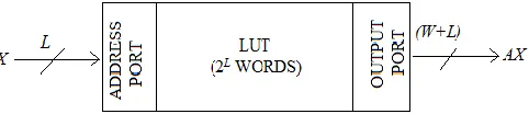
Fig. 1. Conventional Memory-Based multiplier
In the transposed form, a single segmented-memory core could be used rather than different memory modules for individual multiplications in order to avoid the use of individual decoders for each of those separate modules.
II LUT OPTIMIZATION OF MEMORY
BASED MULTIPLICATION
A. OMS Technique to Optimize LUT’S
Fig.1 shows the memory- based multiplication. Let A be a fixed coefficient and X be an input word, say multiplicand. Suppose X is an unsigned binary number of word-length L, there can be 2L possible values of X, and ultimately 2L possible values of product C, where C is the product of A
and X. Therefore, for the conventional
implementation a memory unit of 2L words is necessary which can be used as look-up-table consisting of pre-computed product values which corresponds to all possible values of X. The product A · Xi, for 0 ≤ Xi ≤ 2L − 1, is the same as the binary value of Xi and is stored at the memory location, in such a way that if Xi is used as address for the memory-unit from L-bit binary value, then the corresponding product value is read-out from the memory.
By this, we can design a W-bit coefficient by the following strategy.
1) [(2L/2) +1] words of memory unit with a width of (W + L)-bit is used to store the product values. Here (2L/2) words are odd multiples of A, and the last word is zero.
2) For deriving all the even multiples of A, a barrel shifter is used which produces a maximum of (L−1) left shifts.
3) An address encoder is used to map from L- bit to (L-1) - bit, and control circuit for controlling the bits that has come from barrel shifter.
Table I: LUT Values For Input Word Length L =5
In Table I, A× (2i +1) are the eight odd multiples, which are stored at eight memory locations as Pi, where I ranges from 0-7. By performing left- shift operations of A, we derive first three even multiples of A. Likewise, by left shifting 3A; 6A and 12A are derived , while 10A and 14A are derived by left shifting 5A and 7A, respectively. The word to be stored for X = (00000) is 16A, which we is derived from A by four left shifts using a barrel shifter. However, if 16A is not taken from A, three left shifts is sufficient to obtain all other even multiples of A.
Input X Product Input X Product Address X'
Table II: Encoded Words for X = (00000) AND (10000)
A two-stage and three-stage logarithmic barrel shifter is used for implementing three bit shifts. Hence, by storing 2A for input X = (00000), the product 16A can be derived by three arithmetic left shifts efficiently. Table II shows the product values and encoded words for input words X = (00000) and (10000).The desired encoded word 16A for X = (00000) is derived by shifting 3-bit left of 2A [stored at address (1000)]. When X = (10000), the APC word “0” is obtained by an active-high RESET signal at the output of the LUT given by-
Reset =
X0X1X2X3
X4(1) A simple set of mapping relations is done in Table I and II to map 5-bit input word X into a
4-bit LUT address (d3d2d1d0) .
di X"i1 for i =0,1 , 2 and d3 X"0
(2)
When we shift out all the main zeroes of X by an arithmetic right shift and then address map, X” = (x3”x2”x1”x0”) is generated-
X” = YL IF X4 = 1 or Y’L IF X4=0
(3)
where YL and YL’are derived by circular shifting
of all the main zeros of XL and XL’, respectively.
Fig. 2: Modified OMS LUT Design for fixed Coefficient A
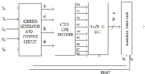
B. Implementation of OMS method
The APC–OMS combined design mentioned here is the LUT for L =5 and for width W which consists of LUT with 9X(W +4)-bit width, a 4-TO-9 line address decoder, an address generation circuit, a barrel shifter, and a control circuit for generating the RESET and control word signal (s1s0) for the barrel shifter [5].
The values of A×(2i +1) that are computed earlier
are stored as Pi, where i ranges from 0 to 7, at the
eight consecutive locations of the memory array, as shown in Table I, whereas; to store 2A for input X = (00000) at LUT address “1000,” as given in Table II. The 4-bit address is taken from the address generator and nine word-select
signals is generated, i.e., {wi ,for 0≤ i ≤8}, where
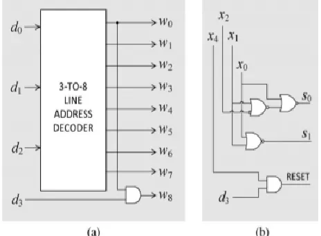
the referenced word from the LUT is selected. Fig. 3(a) shows 4-to-9 line decoder as a simple modification of 3-to-8 line decoder. The control
circuits generate control bits s0 and s1 used by the
barrel shifter to produce shifts to the output of the LUT according to the relations-
0 1 2
0 x x x
S
(4)
0 1
1 x x
S
Note that (s1s0) is a 2-bit binary equivalent of the required number of shifts specified in Tables I and II. The equation for RESET signal given in equation (4) can be alternatively generated by adding AND gate between d3 and x4. Fig. 3(b) shows how to generate control word and RESET. The address-generator circuit receives the 5-bit input operand X and maps that onto the 4-bit address word (d3d2d1d0), according to (2) and (3). A simplified address generator is presented
later in this section.
Fig. 3 (a) Four-to-nine-line address-decoder. (b) Control circuit for generation of s0, s1, and
RESET
Fig. 4(a) Implementation of the sign modification
of the odd LUT output.
(b) Address-generation circuit.
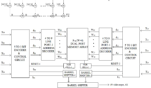
III DESIGNING OMS USING DUAL
PORT METHOD
Multiplication of a 10-bit input with a W-bit fixed coefficient can be performed through a pair of multiplications using two ports where the memory is of 10 words (or two single-port memory units) with that a pair of decoders, encoders, NOR cells and barrel-shifters as given in Fig.5. The shift-adder per forms left shift operation of the output of the barrel-shifter corresponding to more significant half of input by FIVE bit-locations, and adds that to the output of the other barrel-shifter.
IV MEMORY-BASED STRUCTURES
FOR
FIR FILTER USING LOOK-UP-TABLE-MULTIPLIERS
Here we realize a memory- based an N-tap FIR filter by deriving and the memory-cell is designed that has to be used as LUT in the structure. The relationship of an N-tap FIR filter in time-domain is given by-
) 1 ( ). 1 ( ... ) 2 ( ). 2 ( ) 1 ( ). 1 ( ) ( ). 0 ( )
(n h xn h xn h xn hN xnN y
(6) where h(n), for n =0, 1,..., N − 1, gives the filter coefficients, while x(n) and y(n), for n
=0,1,...,N− 1,respectively,represent (N−1)
immediate samples for input and output. Multipliers with memory is used to implement signed as well as unsigned operands. For signed operands, 2’s complement representation is needed to store the input words and product values. The LUT-based multiplication have a
simpler implementation with unsigned
multiplicands because the stored product values
require sign-extension in case of two’s
Equation 2, the recursive computation of the output of FIR filter is represented in the form of data-flow graph (DFG) shown in Fig.6 It consists of N multiplication nodes (M) and (N −1) add-subtract (AS) nodes.
Fig 6: The logical structure of an FIR filter
An L-bit unsigned input has to be multiplied with a magnitude of W-bit of fixed filter-weight, and the same has to be performed conventionally by each of the multiplication-nodes of the DFG.
Fig. 5: Memory-based multiplier structure using dual-port method
AS nodes (N −1) of the DFG is mapped to an add-subtract (AS) cell along with a neighboring delay element. Fig 7 shows a fully pipelined structure of N-tap FIR filter for input word-length L =8, which is derived from Fig.6.
Fig. 7: Conventional LUT-multiplier-based structure
negativity of the weight of the filter. Moreover, the SA cell corresponds to the delays of the DFG of Fig. 6. The FIR filter structure of Fig. 7 takes one input sample and gives one output in each cycle.
Fig.8: Structure of each LUT-multiplier.
A. Implementation of FIR filter by using LUT multiplier
The memory-base structure of FIR filter (for 8-bit inputs) using the proposed LUT design is shown in
Fig. 9. Two design aspects of FIR filter differs from conventional memory based structure.
1) Odd-multiple-storage LUT is used in the place of conventional LUT-multiplier, So that the L-bit word can be multiplied by implementing (2L/2)/2 words storage in LUT of dual-port memory.
2) In Fig. 8, N LUT-multipliers were used by all pair of same address word X1 and X2, One memory module with N segments can be used instead of N modules. If all the multiplications are performed by a one memory module, the complexity of hardware 2(N −1) decoder circuits (used in Fig. 8) could be eliminated. As shown in Fig 9, the proposed structure FIR filter structure consists of a single memory-module and an array consists of N shift-add (SA) cells and (N −1) AS cells and a unit delay.
Fig. 9: Structure of Nth order FIR filter using proposed LUT-multiplier
The memory module structure Fig 9 is similar to that of Fig. 6. Like the structure of Fig. 9, to generate the select signal word and control signal for the dual-port memory core it uses of a pair of encoders and control circuits and a decoders The dual-port memory core (shown in Fig 10) consists of [8×(W+4)]×N array of bit-level memory-elements arranged in 8 rows of [(W
+4)N]-bit width. Every row of this memory consists of N segments, where segment is (W +4)-bit wide for each. The segment of this dual-port core size is 8×(W
+ 4), so ith memory segment stores the 8 words which
X2 are derived from the recent input sample x(n) and given as input to pair of 4-to-3 bit line encoders and control circuits, which generates two sets of word-select signals (WS1 and WS2), a set of control signals ((s01,s00) and (s11,s10)), and two reset signals.
Fig 10: The dual-port segmented memory core for nth order FIR filter.
These all signals are given to the dual-port core as shown in Fig 9. N segments of the memory-core produce N pairs of respected output, those are given as input to the N pairs of barrel-shifters through the 2N NOR cells. The barrel shifter array of N pairs thus produce N pairs of output (h(i)·X1,h(i)·X2) for 0 ≤ i ≤ N −1. The function and structure of the barrel shifter and NOR cell are the same as those discussed before In Fig 9, one input sample has the same number of cycles of latency as the structure of Fig. 7 and this is taken in each clock cycle by FIR filter. In Fig. 8, only one memory module with N segments is used as X1 and X2 has same address words.
The LUT-multiplier-based structure consists of dual-port segmented memory core of size [16× (W+4)] × N, where N is the size of the segment given by [16×(W +4)]. Here only a pair of 4-to-16 lines decoders receives an 8-bit input sample in each cycle, and provides a pair of 16-bit word select signals WS1
and WS2 to the core of the memory. The throughput and latency for each cycle of this structure are the same as that of Fig. 9.
V RESULTS AND ANALYSIS
VERILOG HDL is used in this proposed LUT multipliers. Here the implementation of LUTs is done by the Wallace tree and ripple carry array. The multipliers with same addition schemes are synthesized with this technology library.
Fig. 11: RTL view of APC-OMS Technique by using Dual ports method
Fig 12: Behavioral simulation of the OMS technique
Fig. 13: RTL view of Fir Filter by using LUT method
Fig.14: Behavioral simulation of the Filter by using LUT method
Table III shows the LUT analysis based on the synthesis results.. It is found that the proposed LUT design involves less area and less time to multiply for higher word sizes. Area delay product is saved by more than 30% and 50%, respectively for L = W = 16, and 32 bits compared to CSD multiplier.
Table III. LUT Analysis
The Memory based LUT multiplier has been designed by Xilinx and the analysis has been done between Number of LUT’s of APC and Modified OMS
technique compared to conventional multiplier. Optimization of LUTs takes place to as low as factor
four when compared to the method used
conventionally.
The Memory based LUT multiplier has been designed by Xilinx and the analysis has been done between Area, Delay(ns) and Power(W). LUT multiplier is designed by basic gates and universal gates. The following Table IV shows the comparison between both basic and universal gates. When LUT multiplier is design by basic gates the area and delay were more but the same design were performed by using
universal gates apparently there is decrease in area and delay.
Table IV. ADP Analysis of LUT Multiplier
Table V. ADP analysis of FIF filer by using LUT Multiplier
Comparison of ADP for FIR filter is using LUT Multiplier
word size 16-tap
Design using basic gates
Design using Universal gates Are
a
Dela y
Powe r
Are a
Dela y
Powe r
L=4 150 6.225 0.112 145 5.895 0.112
L=8 239 10.22 0.166 237 9.187 0.166
Number of LUT's Word
Size conventional
APC Technique
Modified OMS
L=5 88 45 24
L=10 320 188 98
Comparison of ADP For LUT Multiplier
word size
Design using basic gates
Design using Universal Gates
Area Delay Power Area Delay Power
L= 5 48 6.217 0.014 40 4.921 0.014
VI CONCLUSIONS
An efficient approach is thus specified for optimizing the LUTs and is implemented through AOMS method that results in improving performance. FIR filter, resembling the Matched filter structure is thus implemented through the design that is applicable for many applications especially for spectrum sensing in cognitive radio of SDR. The specified method and the design process thus provide 20% savings of area-delay product and the throughput is twice that of the previous methods. This is shown in tabular re-presentations and explained briefly in the above sections. The overall implementation process is thus simulated using XILINX ISE Project Navigator and the simulated result is shown. The FIR filter is implemented at the receiver part of the system. To further enhance the system performance by utilizing the available spectrum efficiently the specified method will be implemented at transmitter part of the system.
REFERENCES
[1] J. G. Proakis and D. G. Manolakis, Digital Signal Processing: Principles, Algorithms and Applications. Upper Saddle River, NJ: PrenticeHall, 1996.
[2] G. Mirchandani, R. L. Zinser,Jr.,and J. B. Evans, “Anew adaptive noise cancellation scheme in the presence of crosstalk [speech signals],” IEEE Trans. Circuits and Systems II: Analog and Digital Signal Processing, vol. 39, no. 10, pp. 681–694, Oct. 1995.
[3] D. Xu and J. Chiu, “Design of a high-order FIR digital filtering and variable gain ranging seismic data
acquisition system,” in 1993 IEEE Proceedings Southeastcon’93, Apr. 1993, p. 6.
[4] K. K. Parhi, VLSI Digital Signal Procesing Systems: Design and Implementation. New York: John Wiley & Sons, Inc, 1999.
[5]H.H.Kha,H.D.Tuan,B.-N.Vo,andT.Q.Nguyen,“Symmetricorthogonal
complex-valued filter bank design by semidefinite programming,” IEEE Transactions on Signal Processing, vol. 55, no. 9, pp. 4405–4414, Sept. 2007.
[6] H. H. Dam, A. Cantoni, K. L. Teo, and S. Nordholm, “FIR variable digital filter with signed power-of-two coefficients,” IEEE Transactions on Circuits and Systems I: Regular Papers, vol. 54, no. 6, pp. 1348– 1357, June 2007.
[7] R. Mahesh and A. P. Vinod, “A new common subexpression elimination algorithm for realizing low-complexity higher order digital filters,”IEEE
Transactions on Computer-Aided Design of
Integrated Circuits and Systems, vol. 27, no. 2, pp. 217–229, Feb. 2008.
[8] International Technology Roadmap for
Semiconductors. [Online]. Available:
[10] K. Itoh, S. Kimura, and T. Sakata, “VLSI memory technology: Current status and future trends,” in Proc. 25th European Solid-State Circuits Conference,ESSCIRC ’99, Sept. 1999, pp. 3–10.
[11] T. Furuyama, “Trends and challenges of large scale embedded memories,” in Proc. IEEE 2004 Conference on Custom Integrated Circuits, Oct. 2004, pp. 449–456.
[12] D. G. Elliott, M. Stumm, W. M. Snelgrove, C. Cojocaru, and R. Mckenzie, “Computational RAM: implementing processors in memory,” IEEE Trans. Design & Test of Computers, vol. 16, no. 1, pp. 32– 41, Jan. 1999.
[13] H.-R. Lee, C.-W. Jen, and C.-M. Liu, “On the design automation of the memory-based VLSI architectures for FIR filters,” IEEE Trans. Consumer Electronics, vol. 39, no. 3, pp. 619–629, Aug. 1993.
[14] S. A. White, “Applications of the distributed arithmetic to digital signal processing: A tutorial review,” IEEE ASSP Magazine, vol. 6, no. 3, pp. 5– 19, July 1989.
[15] M. Mehendale, S. D. Sherlekar, and G. Venkatesh, “Area-delay tradeoff in distributed arithmetic based implementation of FIR filters,” in Proc.