Available online:
http://edupediapublications.org/journals/index.php/IJR/
P a g e | 2 1 3Efficient Power Utilization in High Frequency CMOS
Digital Circuits using MTCMOS Technology
1
T.Savitha,
[email protected]
2
N.Nanda Ganesh Kumar,
[email protected]
1
Assistant Professor, ECE Department
1Swamy Vivekananda Institute of Technology
Mahabub College Campus, Secunderabad-500003.
A bs tract :
This paper enumerates low power, high speed design of flip-flop having less number of transistors and only one transistor being clocked by short pulse train which is true single phase clocking (TSPC) flip-flop. Compared to Conventional flip-flop, it has 5 Transistors and one transistor clocked, thus has lesser size and lesser power consumption. It can be used in various applications like digital VLSI clocking system, buffers, registers, microprocessors etc. The analysis for various flip flops and latches for power dissipation and propagation delays at 0.13μm and 0.35μm technologies is carried out. The leakage power increases as technology is scaled down. The leakage power is reduced by using best technique among all run time techniques viz. MTCMOS. Thereby comparison of different conventional flip-flops latches and TSPC flip-flop in terms of power consumption, propagation delays and product of power dissipation and propagation delay with DSCH and Microwind simulation results is presented. Keywords
Multi-Threshold Voltage CMOS (MTCMOS), Static Power Consumption, Propagation Delay, TSPC Flip-flop.
1.
Introduction
The growing market of portable (e.g., cellular phones, gaming consoles, etc.), battery-powered electronic systems demands microelectronic circuits design with ultra-low power dissipation. As the integration, size, and complexity of the chips continue to increase, the difficulty in providing adequate cooling might either add significant cost or limit the functionality of the computing systems which make use of those integrated circuits. As the technology node scales down to 65nm there is not much increase in dynamic power dissipation. However the static or leakage power is same as or exceeds the dynamic power beyond 65nm technology node.
Hence the techniques to reduce power dissipation is not limited to dynamic power. In this article we discuss circuit and logic design approaches to minimize Dynamic, Leakage and Short Circuit power dissipation. Power optimization in a processor can be achieved at various abstract levels. System/Algorithm/Architecture have a large potential for power saving even these techniques tend to saturate as we integrate more functionality on an IC. So optimization at Circuit and Technology level is also very important for miniaturization of ICs.
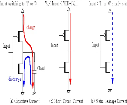
Total Power dissipated in a CMOS circuit is sum total of dynamic power, short circuit power and static or leakage power. Design for low-power implies the ability to reduce all three components of power consumption in CMOS circuits during the development of a low power electronic product. In the sections to follow we summarize the most widely used circuit techniques to reduce each of these components of power in a standard CMOS design. Input switching to '1' or '0'
charge
discharge
Input
Cload
Vthn< Input < VDD-|Vthp|
Input
Input : '1' or '0' steady state
Input
(a) Capacitive Current (b) Short Circuit Current (c) Static Leakage Current
Figure 1: Three components of power in Cmos Circuit
Components of Power in CMOS circuit Ptotal = CLVDD2 + tscVDDIpeak + VDDIleakage
Available online:
http://edupediapublications.org/journals/index.php/IJR/
P a g e | 2 1 4 to reduce cost and power consumption. Withever-reducing gate delays, increasingly larger number of high frequency digital functions prefer CMOS circuits that swing completely between the rails. These circuits scale readily and lend themselves to easier implementation compared with those that work under limited swings. While achieving the required functions with minimal power dissipation is always desirable, this is highly important overall operating conditions in mobile RF applications to reduce recharge cycles.
Variations in process corners reduce the advantages gained through technology scaling and this is predicted to get worse in the future [1]. Changes in temperature and supply voltage also affect cell delays significantly. Raising the current consumption to accommodate the large spread in cell delays is the straightforward but inefficient solution.
This work proposes a circuit technique that reduces the spread in delay and power consumption and applies it to a frequency divider used in RF frequency synthesizers. In general, any standard CMOS digital circuit could be made efficient and robust through the proposed approach.
Multi-threshold CMOS (MTCMOS) is a variation of CMOS chip technology which has transistors with multiple threshold voltages (Vth) in order to optimize delay or power. The Vth of a MOSFET is the gate voltage where an inversion layer forms at the interface between the insulating layer (oxide) and the substrate (body) of the transistor. Low Vth devices switch faster, and are therefore useful on critical delay paths to minimize clock periods [clarification needed]. The penalty is that low Vth devices have substantially higher static leakage power. High Vth devices are used on non-critical paths to reduce static leakage power without incurring a delay penalty. Typical high Vth devices reduce static leakage by 10 times compared with low Vth devices. [1]
One method of creating devices with multiple threshold voltages is to apply different bias voltages (Vb) to the base or bulk terminal of the transistors. Other methods involve adjusting the gate oxide thickness, gate oxide dielectric constant (material type), or dopant concentration in the channel region beneath the gate oxide.
A common method of fabricating multi-threshold CMOS involves simply adding additional photolithography and ion implantation steps.[2] For a given fabrication process, the Vth is adjusted by altering the concentration of dopant atoms in the channel region beneath the gate oxide. Typically, the concentration is adjusted by ion implantation method. For example, photolithography methods are
applied to cover all devices except the p-MOSFETs with photoresist. Ion implantation is then completed, with ions of the chosen dopant type penetrating the gate oxide in areas where no photoresist is present. The photoresist is then stripped. Photolithography methods are again applied to cover all devices except the n-MOSFETs. Another implantation is then completed using a different dopant type, with ions penetrating the gate oxide. The photoresist is stripped. At some point during the subsequent fabrication process, implanted ions are activated by annealing at an elevated temperature.
In principle, any number of threshold voltage transistors can be produced. For CMOS having two threshold voltages, one additional photo masking and implantation step is required for each of p-MOSFET and n-MOSFET. For fabrication of normal, low, and high Vth CMOS, four additional steps are required relative to conventional single-Vth CMOS.
2.
Design and Implementation
A common implementation of MTCMOS for reducing power makes use of sleep transistors. Logic is supplied by a virtual power rail. Low Vth devices are used in the logic where fast switching speed is important. High Vth devices connecting the power rails and virtual power rails are turned on in active mode, off in sleep mode. High Vth devices are used as sleep transistors to reduce static leakage power.
The design of the power switch which turns on and off the power supply to the logic gates is essential to low-voltage, high-speed circuit techniques such as MTCMOS. The speed, area, and power of a logic circuit are influenced by the characteristics of the power switch.
In a "coarse-grained" approach, high Vth sleep transistors gate the power to entire logic blocks. [3] The sleep signal is de-asserted during active mode, causing the transistor to turn on and provide virtual power (ground) to the low Vth logic. The sleep signal is asserted during sleep mode, causing the transistor to turn off and disconnect power (ground) from the low Vth logic. The drawbacks of this approach are that:
• Logic blocks must be partitioned to determine when a block may be safely turned off (on)
• Sleep transistors are large and must be carefully sized to supply the current required by the circuit block
Available online:
http://edupediapublications.org/journals/index.php/IJR/
P a g e | 2 1 5 In a "fine-grained" approach, high Vth sleeptransistors are incorporated within every gate. Low Vth transistors are used for the up and pull-down networks, and a high Vth transistor is used to gate the leakage current between the two networks. This approach eliminates problems of logic block partitioning and sleep transistor sizing. However, a large amount of area overhead is added due both to inclusion of additional transistors in every Boolean gate, and in creating a sleep signal distribution tree.
An intermediate approach is to incorporate high Vth sleep transistors into threshold gates having more complicated function. Since fewer such threshold gates are required to implement any arbitrary function compared to Boolean gates, incorporating MTCMOS into each gate requires less area overhead. Examples of threshold gates having more complicated function are found with Null Convention Logic and Sleep Convention Logic Some art is required to implement MTCMOS without causing glitches or other problems.
Figure 2: Basic MTCMOS design
To achieve the goal of having high performance and low power consumption flip flops, we use the following dynamic techniques in our design methodology –power gating, clock gating and data retention cell.
a.
Power Gating
The low threshold voltage transistors are power gated, i.e., they are stacked in series with high threshold voltage devices, called gating transistors that connects them to the power supply and the ground. The gating transistors are turned on during the active mode and are turned off during the sleep mode, which cuts off the critical path from supply
voltage or ground thereby reducing the leakage current tremendously. The gating transistors should be wide enough to provide enough current to the devices in the critical path during the active mode. Power gating can be done in two ways —distributed power gating and centralized power gating [2]. The distributed power gating uses individual footer and header switches for each cell while the centralized gating uses a single header/footer for multiple cells. Though it is easier to implement the distributed power gating and it more immune to voltage droops and ground bounce, it comes with the area overhead and can degrade the performance due to stack effect [2]. Also, the centralized gating can take advantage of the fact that the leakage paths are mutually exclusive and hence spares them from being extremely large. Whether to choose one type of gating over the other depends on the circuit to be implemented in order to avoid the sneak leakage paths [3]. Usually, the circuits where the circuitry for data storage is isolated, coarse gating can be used [2].
b.
Clock Gating
The clock gating masks the clock signal when the circuit is not performing useful computation [4]. It uses an enable control signal from the circuit to control the clock signal during the sleep mode. In our design we used a NOR gate as the combinational circuit to generate the gated clock signal and the inputs to the NOR gate are clock bar and sleep signal.
c.
Data Retention Cell
The current sequential circuit designs do not focus on maintaining the state of the flip-flop while moving to the sleep mode. However, it is important for the flip-flop devices to maintain their state while they are in the sleep mode and retrieve it after coming out of the sleep state. For this, a special data retention circuitry is required. This circuitry should be such that it does not increase the leakage during the sleep mode and at the same time does not degrade the performance while in the active mode. It is also essential that it utilize the circuitry and the control signals from the current design for storing the data [2]. It keeps the circuit simple, as it does not require any additional circuitry and control signals. This reduces the extra capacitive load on the critical path, thereby making the circuit faster.
3.
Framework
Available online:
http://edupediapublications.org/journals/index.php/IJR/
P a g e | 2 1 6 NAND gate depending on the specific signalrequirement during sleep mode.
Figure 3: Block diagram
a.
Flip-flop structures
i. Ps eudo-static M TCM OS flip -flo p with o u ter feed b ack
An outer feedback path controlled by sleep signal is added to traditional master-slave flip-flop. Feedback path (SLEEP transmission gate) becomes active during sleep mode and forms a static latch reusing the inner feedback circuit to store state. Low threshold transistors are on the critical path and are gated with high threshold transistors in a distributed mode. The feedback path is implemented with high threshold transistors. The circuit schematic is shown in Fig.2.
Figure 4 Pseudo-static MTCMOS flip-flop with outer feedback [2]
ii. C2M OS static M TCM OS flip -flo p with o u ter
feed b ack
In this flip-flop, the non-feedback part is gated in a centralized manner, which reduces the total width of the gating transistors. During sleep mode, state is saved with the inverting feedback on nodes isolated from the critical path, which allows the use of centralized gating without the risk of having possible sneak leakage current path. The circuit schematic is shown in Fig. 3.
Fig.5 C2MOS static MTCMOS flip-flop with
outer feedback [2]
iii. M aster-sid e M TCM OS flip -flo p with o u ter feed b ack
In this circuit, outer feedback is added only on the master side of the master- slave flip-flop to latch state during sleep mode, and only one inner feedback inverter is reused. The critical path is gated in the centralized manner. The circuit schematic is shown in Fig.4.
Fig.6 Master-side MTCMOS flip-flop with outer feedback [2]
iv . Co n v en tio n al M TCM OS flip -flo p with d ata p res erv in g s leep mo d e
Available online:
http://edupediapublications.org/journals/index.php/IJR/
P a g e | 2 1 7 Fig.7 Conventional MTCMOS flip-flop with datapreserving sleep mode [5]
v. SRA M M TCM OS flip -flo p
In this flip-flop, critical path is gated to the ground through one centralized NMOS sleep switch. A data retention cell, which is similar to a standard 6T SRAM cell used in caches, is added to the slave latch through two high threshold NMOS pass transistors. The data retention cell is controlled by a sleep transmission gate, and retains the last data sampled by the master latch when clock transitions low. At the end of sleep mode, sleep signal transitions high before clock is enabled. Depending on the data stored in the data retention cell, either SRAM-node3 or the output node is discharged to achieve data retrieving. Clock signal is then enabled and the whole flip-flop is reactivated. The circuit schematic is shown in Fig.8.
Fig.8 SRAM MTCMOS flip-flop [5]
b.
Metrics Analysis
Metrics analyzed for the five reference flip-flops are setup time, leakage power, and estimated area, as listed in Table.1. Leakage power is calculated for
input-output pattern of DQ=00 as an example of illustration. Area is estimated with the total width of the transistors, which have a minimum length decided by the technology.
Tab le 1. Metrics analysis for reference flip -flo p s
Setu p time (p s )
Leakag e p o wer (DQ=00, W )
Es timated area (n m)
1 12.0 3.597e-9 14580
2 16.3 2.681e-9 19980
3 30.4 34.21e-12 18090
4 3.0 19.91e-12 14310
5 1.0 9.515e-15 11610
From the metrics analysis, SRAM flip-flop is seemingly advantageous over the other four in that a great drop in setup time, leakage power, and area is seen. However, due to the fact that it is holding the state in a data retention cell away from the critical path, extra signal design is required for data retrieving before activating the flip-flop.
Leakage current scaling with the power supply is shown in Fig.7. Situations with different input-output patterns are taken into consideration.
Available online:
http://edupediapublications.org/journals/index.php/IJR/
P a g e | 2 1 8 (c) DQ=10 (d) DQ=11Fig. 9 Leakage current of the reference flip-flops during sleep mode
4.
Proposed MTCMOS flip-flop designs
Based on the design methodologies illustrated in the previous part, two MTCMOS flip-flops with outer feedback are proposed.
a.
Flip-flop structures
i. Ris ing-edge MTCMOS flip-flop with slave-side o u ter feed b ack d es ig n 1
Fig.10 Proposed MTCMOS flip-flop design 1
In the proposed MTCMOS flip-flop design 1, critical path is constructed with low threshold transistors, which ensures fast operation as compared to single threshold flip-flop during active mode. Transistors away from the critical path have high threshold that helps reduce leakage. Low threshold transistors are power gated with sleep transistors in a centralized manner. The feedback path of the slave latch is reused in the outer feedback to retain data during sleep mode. The output node is in the data retention loop, which helps avoid extra data retrieving process and avoid slowing down the flip-flop operation when coming out of the sleep mode.
ii. Ris ing-edge MTCMOS flip-flop with slave-side o u ter feed b ack d es ig n 2
Fig.11 Proposed MTCMOS flip-flop design 2 In the proposed MTCMOS flip-flop design 2, one inverter and two transmission gates controlled by gated clock signal are added on the slave side to form a static latch aiming at storing states during sleep mode. Similarly, as the proposed design 1, extra data retrieving structure is avoided due to the fact that the output node is on the data retention loop. Two transmission gates are used to separate the added half loop to make sure that the data retention part would not influence the main path during active mode.
b.
Metrics Analysis
Metrics including Clock to Q delay, setup time, leakage power, and estimated area are analyzed and listed in Table.2.
Tab le 2. Metrics analysis for proposed flip -flo p s
Clo ck to Q d elay
(p s )
Setup time (p s )
Leakag e p o wer (DQ=00,
W )
Es timated area (n m)
1 25.34 1.86 3.597e-9 12420
Available online:
http://edupediapublications.org/journals/index.php/IJR/
P a g e | 2 1 9 The proposed design 2 circuit has the smallestarea overhead among the seven flip-flops studied in this paper. But delay metrics are somehow sacrificed.
Leakage current during sleep mode is analyzed and compared to single threshold flip-flop that has the same structure and sizing. As is shown in Fig.10, the leakage sees a drastic decrease for any input-output pattern.
.
Fig.12 Leakage current comparison between the MTCMOS flip-flop and corresponding single
threshold flip-flop
5.
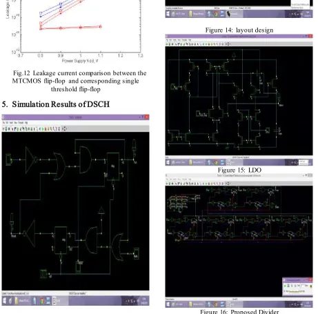
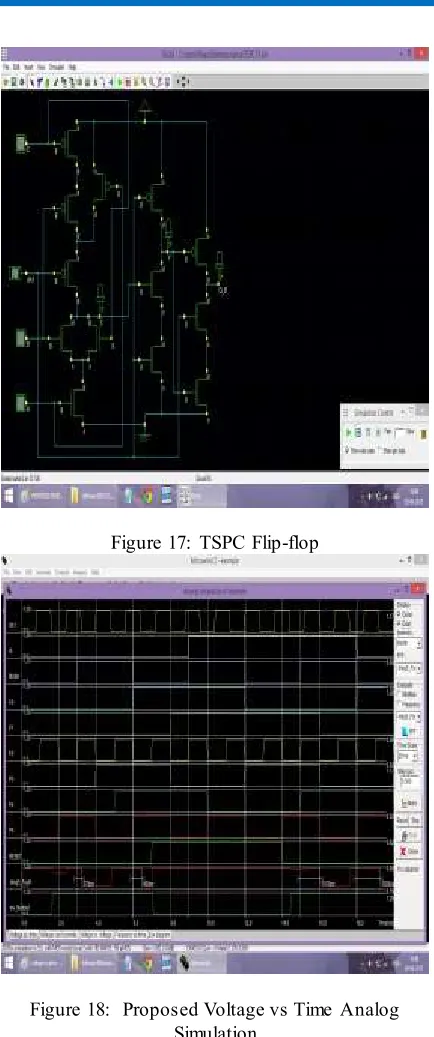
Simulation Results of DSCH
Figure 13: cell 2/3 design
Figure 14: layout design
Figure 15: LDO
Available online:
http://edupediapublications.org/journals/index.php/IJR/
P a g e | 2 2 0 Figure 17: TSPC Flip-flopFigure 18: Proposed Voltage vs Time Analog Simulation
Figure 19: Sample Voltage vs Time Simulation
6.
Conclusion
The sub-optimal utilization of power in standard CMOS digital circuits was analyzed. A technique to improve power efficiency was demonstrated using the example of the frequency divider in an RF frequency synthesizer. It was shown that operating digital circuits with replica bias derived from a similar low-power module manages to keep the power consumption close to the minimum possible over manufacturing and operational variations. An additional favorable result was improvement in immunity from supply noise.
MTCMOS is one of the important low power techniques and is used to reduce the leakage. To reduce leakage power in MTCMOS circuits, sleep and sleep bar transistors are high threshold voltages. When sleep input is OFF and sleep bar input is ON, there is no current flow in the low threshold voltage main circuit. When sleep is ON and sleep bar is OFF then the circuit works in normal mode.
7.
References
[1]Y. Cao and L. Clark, “Mapping statistical process variations toward circuit performance variability: An analytical modeling approach,” Computer-Aided Design of Integrated Circuits and Systems, IEEE Transactions on, vol. 26, no. 10, pp. 1866– 1873, 2007.
[2]C. Vaucher, I. Ferencic, M. Locher, S. Sedvallson, U. Voegeli, and Z. Wang, “A family of low-power truly modular programmable dividers in standard 0.35µm cmos technology,” Solid-State Circuits, IEEE Journal of, vol. 35, no. 7, pp. 1039–1045, 2000.
[3]V. V. Ivanov and I. M. Filanovsky, Operational amplifier speed and accuracy improvement. Kluwer academic publishers, 2004, section 3.5. [4]M. A. T. Sanduleanu and J. Frambach, “1GHz
tuning range, low phase noise, LC oscillator with replica biasing common-mode control and quadrature outputs,” in Solid-State Circuits Conference, 2001. ESSCIRC 2001. Proceedings of the 27th European, 2001, pp. 506–509. [5]J. Maneatis, “Low-jitter process-independent


![Fig.7 Conventional MTCMOS flip-flop with data preserving sleep mode [5]](https://thumb-us.123doks.com/thumbv2/123dok_us/7786568.1288390/5.596.71.283.40.306/fig-conventional-mtcmos-flip-flop-data-preserving-sleep.webp)