Abstract—Integration of decoupling capacitors in SiC
MOSFET modules is an advanced solution to mitigate the effect of parasitic inductance induced by module assembly interconnects. In this paper, the switching transient behavior is reported for a 1.2kV SiC MOSFET module with embedded DC-link capacitors. It shows faster switching transition and less overshoot voltage compared to a module using an identical package but without capacitors. Active power cycling and passive temperature cycling are carried out for package reliability characterization and comparisons are made with commercial Si and SiC power modules. Scanning acoustic microscopy images and thermal structure functions are presented to quantify the effects of package degradation. The results demonstrate that the SiC modules with embedded capacitors have similar reliability performance to commercial modules and that the reliability is not adversely affected by the presence of the decoupling capacitors.
Index Terms— SiC, MOSFET module, embedded capacitor,
switching performance, thermo-mechanical reliability
I. INTRODUCTION
N recent years, Silicon Carbide (SiC) MOSFET power modules have been developing rapidly due to the increasing demand of hybrid electric vehicles/electric vehicles (HEV/EV) as well as compact solutions for solar inverters, industrial drives and high frequency power supplies. SiC MOSFETs have lower power losses compared to IGBTs. Hence they offer the potential to increase converter efficiency. As a result, the capacity and cost of the cooling system can be reduced [1]. The improved switching losses enable operation at very high switching frequencies. This allows a reduction in the physical size of magnetic components used in the input/output filter, which in turn reduces the volume and increases the power density of the converter [2]. In addition, the intrinsic body diode can provide the function of anti-parallel diode making it
This work was supported in part by UK Engineering and Physical Science Research Council (EPSRC) through the Centre for Power Electronics [research grant EP/K035304/1] and in part by the Advanced Propulsion Centre UK through the FIRS3T project.
L. Yang is with the Electrical and Electronic Engineering Department, University of Nottingham, UK (e-mail: [email protected]).
K. Li is with the Electrical and Electronic Engineering Department, University of Nottingham, UK (e-mail: [email protected]).
J. Dai is with the Electrical and Electronic Engineering Department, University of Nottingham, UK (e-mail: [email protected]).
possible to reduce the assembly part, which cuts costs and mitigates implied reliability concerns from additional interconnects such as wire bonds and die attach. In order to fully exert potential benefits proffered by wide band-gap semiconductors, integration techniques, commutation process and packaging reliability needs to be compatible with the device development.
With fast switching speed, the stray inductance induced by the bond wires or connection pins could cause overshoot and high-frequency parasitic ringing oscillation on the drain-source voltage or gate-source voltage [3-5]. Various solutions have been proposed in an effort to reduce the switching parasitic inductance in the current commutation pass. These include rearranging substrate copper trace layout and wire pattern, optimizing packaging design with low DC-link inductance or replacement of bond wires and bus bars [5-9]. The other solution is the integration of DC capacitors inside the power module. This configuration provides a low loop inductance for the current commutation loop and thus minimizes the DC-side parasitic inductance [10, 11]. A few recent studies reporting on integrating capacitors in a SiC MOSFET module mainly focused on module design and electrical characterization [12-15]. Thermo-mechanical reliability with respect to module integration was not addressed.
In this work, electrical performance and assembly integration reliability of a 1.2kV SiC MOSFET module with embedded decoupling capacitors is investigated. Switching transient behavior is compared between two modules in the identical package, one with embedded capacitors and the other one without. Active power cycling and passive temperature cycling, supported by transient thermal impedance characterization and scanning acoustic microscopy, are used to evaluate key degradation mechanisms. The thermal structure function is analyzed to elucidate the degradation in the heat flow path
M. Corfield is with the Electrical and Electronic Engineering Department, University of Nottingham, UK (e-mail: martin.corfield@ nottingham.ac.uk).
A. Harris is with Dynex Semiconductor Limited, Doddington Road, Lincoln, UK. (e-mail: [email protected]).
K Paciura is with Cummins Power Generation, Barnack Road, Stamford, UK. (e-mail: [email protected]).
J. O'Brien is with Cummins Power Generation, Barnack Road, Stamford, UK. (e-mail: [email protected]).
C.M Johnson is with the Electrical and Electronic Engineering Department, University of Nottingham, UK (e-mail: [email protected]).
Electrical performance and reliability
characterization of a SiC MOSFET power
module with embedded decoupling capacitors
Li Yang, Ke Li, Jingru Dai, Martin Corfield, Anne Harris, Krzysztof Paciura
,
John O'Brien,
C. Mark Johnson
inside the module. In addition, the capacitance of the integrated capacitor is characterized before and after cyclic stress.
II. ELECTRICALPERFORMANCE
A. Switching Characterization Test Setup
[image:2.595.307.550.83.176.2]The module under study incorporates a three-phase inverter in a single package with a full-bridge configuration and is equipped with integrated DC ceramic capacitors (CeraLinkTM, 0.25µF, 900V) across each phase leg [16]. Each switch is composed of one CREE CPM2-1200-0025B SiC chip (1200V, 98A). Six chips are soldered onto three Direct Bonded Copper (DBC) substrates which are soldered down onto a copper baseplate. There are no anti-parallel diodes enclosed in the module. Dimension of the baseplate is 113mm×55mm. A photo and electrical circuit diagram of the module is presented in Figure 1.
Fig. 1. Photo and electrical circuit diagram of the SiC MOSFET module under study
The switching transient characterization is carried out for two modules, labelled as: PM_1, the module without capacitors and PM_2_Cintthat has integrated capacitors. They are assembled with the identical packaging. Fig. 2 shows the electrical circuit for the measurement of switching current and voltage waveforms. It is mainly constituted by a half bridge with two SiC-MOSFET switches S1 and S2, an inductive load, an external decoupling capacitor (Cdcp) and a bulk capacitor (Cbulk) linking the power supply and Cdcp. Switching characterization is carried out on the switch S1 and S2 is switched off.
Fig. 2. Electrical circuit to measure device switching current and voltage
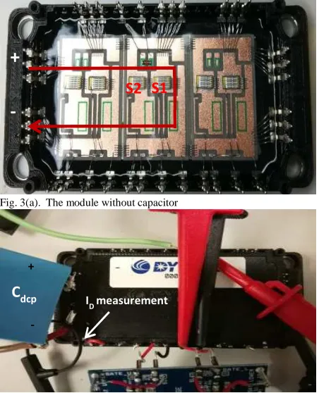
Fig. 3a shows the internal layout of prototype PM_1. As the decoupling capacitor Cdcpis connected externally to the module, a Rogowski coil is attached through the module terminal pins to measure the device switching current ID(Fig. 3b), where the measurement position is indicated as IDin Fig.2
Fig. 3(a). The module without capacitor
Fig. 3(b). Measurement circuit
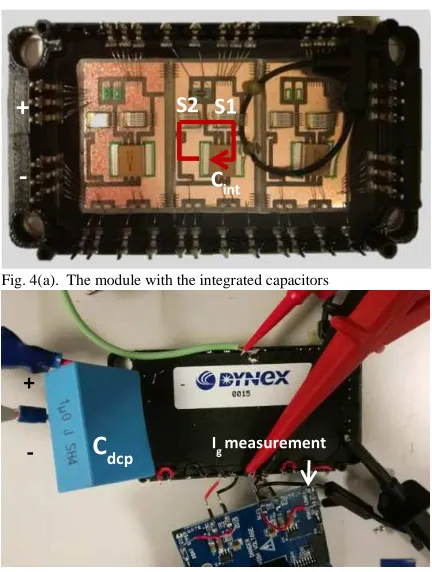
Fig. 4a shows the internal layout of prototype PM_2_Cint. A Rogowski coil is wound around the bonding wires of device S1 in order to measure its switching current. In this condition, the measurement position is indicated as Iloopin Fig. 2, which shows that the current݅ measured by Rogowski coil in the module includes device gate loop current ݅.In order to obtain the device switching current ݅ (݅ൌ ݅െ ݅) and compare it with the above condition, ݅is measured by another identical Rogowski coil as shown in Fig.4b.
+
-S2 S1
C
dcp IDmeasurement
+
[image:2.595.305.531.259.538.2] [image:2.595.45.252.304.556.2]-Fig. 4(a). The module with the integrated capacitors
Fig. 4(b). Measurement circuit
In Fig. 3a and Fig. 4a, the device switching loop is marked with red lines, and it can be seen that the switching loop in the power module that has the integrated capacitors is smaller than the one without capacitors.
B. Comparison in Switching Transients
The used Rogowski coil (CWTUM/06/R) has a bandwidth of 30MHz and peak di/dt measurement rate of 70kA/µs, while the oscilloscope (DPO4104B) has a bandwidth of 1GHz. The switching waveforms of drain current ݅ and drain-source voltageܸௌare recorded at 600V and 30A, which are displayed in Fig. 5. From the turn-on waveforms (Fig. 5(a)), it can be seen that the drain current݅of the PM_2_Cintshows faster damping comparing to PM_1. Also, PM_2_Cinthas a current transition rate of 2.5A/ns, which is faster than PM_1 (2A/ns).
The turn-off waveforms for both modules are presented Fig. 5b. Comparing with PM_1, the overshoot voltage of PM_2_Cint is 108V less. Meanwhile, the resonance frequency at the end of the switching is around 25MHz for PM_1 and 100MHz for PM_2_Cint.
Fig. 5(a). Turn-on transient waveforms
Fig. 5(b). Turn-off transient waveforms
Based on device switching waveforms shown in Fig.5, device switching losses (EONand EOFF) are obtained for the two power modules and they are listed in TABLE 1.
TABLE I
COMPARISON OFEONANDEOFFOFTWOPOWERMODULES
PM_1 without Cint PM_2 with Cint
EON(µJ) 90 450
EOFF(µJ) 607 539
It is found that EOFFof PM_1 is higher than PM_2, because of higher overshoot VDS voltage during device turn-off transition. However, EONof PM_1 is much lower than that of PM_2. This is supposedly due to the snubber effect of increased Lpara value in the power loop of PM_1. At turn-on switching, during the rise of ID, bigger value of Lparagives rise to a higher
voltage dropܮௗ
ௗ௧of device VDSvoltage, which decreases
ID, VDSoverlapping surface and time. This result corresponds with the results between EON, EOFF and Lpara presented by authors in [17] for SiC-MOSFET. The comparison of device switching losses shows that there might be less switching losses of devices in PM_1. However, as device switching loop increases in PM_1, parasitic resistance value is bigger in PM_1 than in PM_2, which causes more losses of the whole current conduction loop in PM_1 than in PM_2.
It needs to be noted that even though PM_2_Cint encloses decoupling capacitors, a Cdcp is still necessary for the measurement in order to avoid lower resonance frequency between Cint and the lumped parasitic inductance Cbulkin the loop (Lpara2+Lpara3shown in Fig.2), which may be observed if loop resistance is inferior to ඥሺܮଶ ܮଷሻȀܥ௧. This
S1
S2
C
int+
-C
dcp Igmeasurement+
[image:3.595.45.261.80.366.2] [image:3.595.304.552.83.365.2]-lower-frequency resonance (݂= ଵ
ଶ∗గ∗ට(ೌೝೌమାೌೝೌయ)∗
) may
lead to another VDS overshoot voltage.More discussions on different resonance frequency observed in device switching can be found in [18]. A comparison of the VDSswitching waveform in PM_2_Cintmodule with and without Cdcpis shown in Fig.6. It can be seen that using a 1µF Cdcphelps to damp the 793 kHz lower frequency resonance.
Fig. 6. Device VDS waveform comparison in PM_2_Cintmodule with and
without Cdcp
In summary, the module with integrated capacitors suppresses the parasitic inductance within the device switching loop which results in faster switching transition and less overshoot voltage. It is worthy pointing out that the Ceralink capacitors, which employ an anti-ferroelectric dielectric, have strong voltage and temperature capacitance sensitivities. However, in this decoupling application, the primary function is to provide a low-impedance, high-frequency return path for the commutation loop, so the actual capacitance value has a relatively small effect on the measured response.
III. RELIABILITYCHARACTERIZATION
A. Passive Temperature Cycling Test 1) Passive Cycling Experimental Setup
The two modules PM_1 and PM_2_Cint was placed in an ESPEC three-zone environmental thermal shock test chamber. The baseplate temperature is ranging from -55°C to +90°C. Each cycle had a period of 20 minutes with a heating time and cooling time at 10 minutes respectively.
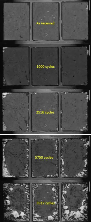
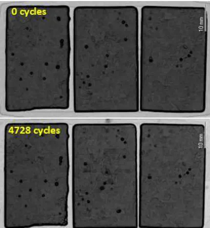
Scanning Acoustic Microscopy (SAM) characterization was carried out using PVA TePla AM300. C-mode scanning (interface scan) was conducted with a 35MHz transducer to provide planar view on several focused depths corresponding to specific internal layers. This creates 2D greyscale images from the reflected ultrasonic echoes, in which discontinuities show different brightness from the intact area. The modules were imaged prior to cycling (in as-received condition) in order to provide a basis for comparison. The same samples were subsequently imaged at 1000, 1490, 2516, 5750 and 9317 cycles.
[image:4.595.307.547.108.183.2]2) SAM Tomography Images and Comparisons
Fig. 7. Schematic cross-section of the module assembly structure
A schematic cross-section of the module assembly structure is presented in Fig. 7. In Fig. 8, SAM images for the substrate ceramic layer are displayed for PM_2_Cint. Growing white area indicates delamination in the module substrate mount-down solder as the temperature cycling progressed. It initiated from the edge of the solder layer and propagated towards center.
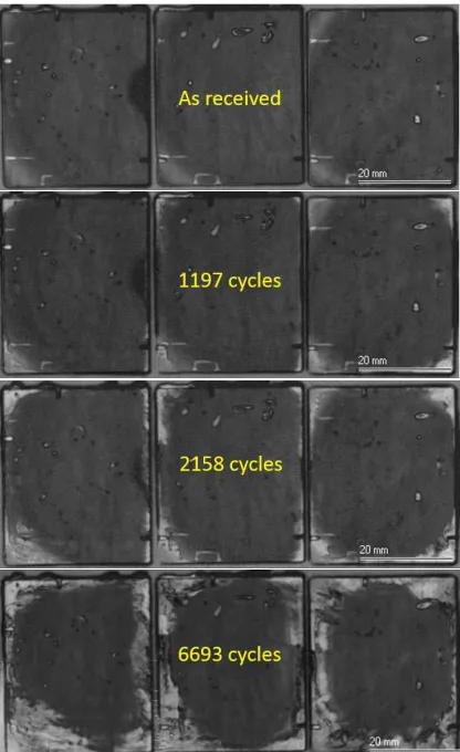
[image:4.595.47.289.188.311.2] [image:4.595.305.486.278.720.2]For comparison, two commercial three-phase Si IGBT modules with similar substrate mount-down structure was subjected to passive cycling over the same temperature regime. Materials and layer thickness of the substrate mount-down layers for Si IGBT and SiC MOSFET prototype modules are listed in Table 2. The SAM images for the substrate ceramic layer is presented in Fig. 9 for one of the commercial IGBT modules.
Fig. 9. SAM images showing delamination of substrate mount-down solder layer for commercial IGBT1 during passive temperature cycling test
TABLE II
MATERIALSANDTHICKNESS OFTHESUBSTRATEMOUNT-DOWN LAYERS FORTHEIGBTANDMOSFET MODULES
Commercial Si IGBT module
SiC MOSFET module prototype Substrate Al2O3(1mm) AlN (1mm)
Substrate mount-down solder
Eutectic SnAg (0.4mm) SnSb5 (0.2mm)
Baseplate Copper (3mm) Copper (2.8mm)
The SAM images are transformed into a binary image in MATLAB where the white pixels indicate attached area on the substrate tile and the black pixels indicate cracked area. In this way, the attached area of the substrate tile mount-down solder can be estimated as a percentage of the total area. Fig. 10 shows the estimated percentage of the attached area of the solder layer
[image:5.595.44.279.605.668.2]at different cycle numbers for the two modules during the cycling test assuming that three substrate tiles are completely attached onto the baseplate before cycling. After 9317 cycles, approximately 57% and 50% solder area remain attached for PM_1 and PM_2_Cint respectively. The evolution of the attached area of substrate mount-down solder for the two commercial IGBT modules shows a similar degradation rate to the two SiC MOSFET module prototypes.
Fig. 10. Estimated attached area of substrate mount-down solder as a percentage of the total area during temperature cycling of -50°C ~ 90°C
3) Characterization of the Embedded Capacitors
To verify the integrity of the embedded decoupling capacitor, the capacitance value was measured before and after cycling using an impedance analyser at 1 kHz and with a DC bias voltage of 0V. Before cycling the measured capacitance is around 137nF and it remained unchanged after 9317 temperature cycles.
B. Active Power Cycling Test
1) Power Cycling Experimental Setup
To further investigate the module packaging reliability, the SiC MOSFET module with embedded capacitors is undertaken power cycling test using a “MentorGraphics” Power Tester 1500A [13]. During cycling, the module was mounted on a water cooled cold plate with a 50µm thick Kapton film as the thermal interface between the cold plate and the baseplate. The use of Kapton film increases the case-to-ambient thermal resistance in order to achieve a larger temperature swing at the substrate-case interface so accelerating degradation of the internal thermal path. Forward voltage drop of the body diode Vf was used as a thermo-sensitive electrical parameter to estimate the module junction temperature. A calibration of Vf as a function of temperature was prepared in advance.
individually. The maximum temperature for the six MOSFETs varies between 137°C and 154°C, while cold plate temperature was maintained at 10°C. An average junction temperature
swing from 21°C to 147°C (ΔT=126°C) was achieved across
the six devices.
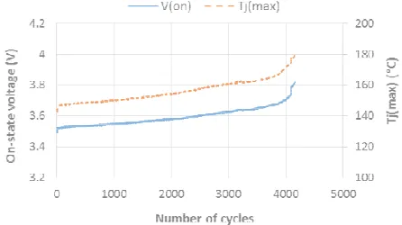
[image:6.595.305.528.83.338.2]The power cycling test was terminated at 4728 cycles when the on-state voltage increased by 16%. Fig. 11 shows the record of on-state voltage and maximum junction temperature for one of the devices throughout the cycling. They kept unchanged until around 3400 cycles. Significant incremental steps started from 4200 cycles. And the staircase nature is known to be the result of wire bond lift-offs [20, 21]. Increase of the on-state voltage leads to an increase of power loss and therefore a rise in the junction temperature.
Fig. 11. Development of one MOSFET on-state voltage during power cycling
[image:6.595.52.285.259.389.2]2) Thermal structure function and SAM tomography imaging Transient thermal impedance measurements and scanning acoustic microscopy were performed at as-received condition, at 1000 and 4728 power cycles. Six chips are heated up together and the thermal characterization is recorded for each chip individually. Cumulative and differential structure functions are extracted for one chip and displayed in Fig. 12. They provide a map of the heat conduction path from junction (at the origin of the resistance axis) to ambient (water) which appears as a vertical lines at the right hand side indicating infinite heat capacitance. The wide flat region is the thermal interface, i.e. kapton film which has a large thermal resistance. The variability of the junction-to-ambient thermal resistant is caused by remounting the module following SAM and also due to the inconsistent heatsink thermal resistance as a result of variable water temperature and the flow rate.
Fig. 12. Structure functions of the PM_2_Cintduring power cycling
However, the junction-to-case thermal resistance Rthjcis not affected by these factors. It can be seen from the graph that junction-to-case resistance stays unchanged after 4728 cycles, indicating no significant reduction of the solder attach area. This agrees with the SAM tomography images of substrate mount-down solder shown in Fig. 13.
Fig. 13: SAM tomography images of the substrate mount-down solder in the PM_2_Cint
[image:6.595.306.511.444.666.2]The module includes six SiC MOSFETs and six SiC Schottky diodes soldered on aluminum nitride (AlN) DBC substrates which are mounted on a Cu baseplate. The anti-parallel diodes were subjected to power cycling. A constant heating current of 115A was applied and shared among three legs so the monitored forward voltage and junction temperature is a global measurement across the whole module. This led to an initial
temperature swing of 13°C ~ 146°C (ΔT=133°C). The module
[image:7.595.305.524.82.209.2]was subjected to 4152 power cycles.
Fig. 14. Development of diode forward voltage during power cycling
Fig. 14 shows the maximum junction temperature and forward voltage (Vf) of the freewheeling diodes during the power cycling test. The forward voltage increased 9% at the end of the test. Before 4000 cycles, it increases gradually indicating growing degradation in the thermal stack. The steep increase at the end of the test is considered to be caused by the wire bond lift-offs.
[image:7.595.59.282.204.329.2]The cumulative and differential structure function is extracted for the whole module and displayed in Fig. 15. It can be seen that the cumulative structure function has shifted to the right as the cycling number increases which accounts for a change in the internal structure of the module resulting in an increase of junction-to-case thermal resistance [22]. In the differential structure function, each peak is related to a different material in the thermal stack and K is a value proportional to the cross-sectional area squared. Right shift of peaks indicates increase of the thermal resistance of the assembly layers.
Fig. 15. Structure functions of the commercial SiC MOSFET module during power cycling
SAM tomography confirms that the degradation took place at the substrate mount-down solder layer, which is shown as the white area in the photo of 4152 cycles (Fig. 16).
Fig. 16. SAM tomography images of the substrate mount-down solder in the commercial SiC MOSFET module
4) Discussion
[image:7.595.306.507.288.477.2]IV. CONCLUSION
In this work, a high power SiC MOSFET module with embedded decoupling capacitors has been studied from the switching and packaging reliability perspective. Switching transient characterization of the module with integrated capacitors showed faster switching transition and less overshoot voltage compared with the same semiconductors in an identical package but without embedded capacitors, indicating suppression of the parasitic inductance within the device switching loop and thus providing favorable conditions for high-frequency operation. During active power cycling tests at comparable temperature swings, the SiC module prototype demonstrated a similar lifetime to the commercial SiC module. However, the two modules are composed of different materials and display different dominant degradation modes. During passive temperature cycling under identical conditions, the substrate mount-down solder in the SiC module prototype showed similar degradation rate as the commercial Si-based IGBT. In addition, the capacitance of the integrated capacitor remained unchanged after cyclic passive temperature stress. Together, the tests demonstrate that the SiC MOSFET module with embedded decoupling capacitors has improved switching behavior and can be expected to display similar levels of thermo-mechanical reliability to commercial power modules.
REFERENCES
[1] R. A. Wood and T. E. Salem, "Evaluation of a 1200V, 800A All-SiC Dual Module,"IEEE Trans. Power Electronics, vol. 26, pp. 2504-2511, 2011
[2] A. Trentin, L. d. Lillo, L. Empringham, P. Wheeler, and J. Clare, "Experimental Comparison of a Direct Matrix Converter Using Si IGBT and SiC MOSFETs,"IEEE J. Emerg. Sel. Top. Power Electron, vol. 3, no. 2, pp.542-554, 2015
[3] M. Meisser, M. Schmenger, T. Blank “Parasitics in Power Electronic Modules: How parasitic inductance influences switching and how it can be minimized”,PCIMEurope 2015, 19 – 21 May 2015, Nuremberg, Germany
[4] O. Alatise, N.-A. Parker-Allotey; D. Hamilton, and P. Mawby, “The Impact of Parasitic Inductance on the Performance of Silicon-Carbide Schottky Barrier Diodes,”IEEE Trans. Power Electronics, vol. 27, no. 8, pp.3826-3833, 2012
[5] R. Bayerer, D. Domes, "Power circuit design for clean switching", 2010 6th International Conference onIntegrated Power Electronics Systems
(CIPS), 16-18 March 2010, pp.1-6
[6] S. Li, L. M. Tolbert, F. Wang, and F. Z. Peng, “Stray inductance reduction of commutation loop in the P-cell and N-cell-Based IGBT phase leg module,”IEEE Trans. Power Electronics, 2014, vol. 29, no. 7, pp. 3616–3624
[7] E. Hoene, A. Ostmann, B. T. Lai, C. Marczok, A. Musing, and J. W. Kolar, “Ultra-Low-Inductance Power Module for Fast Switching Semiconductors, ” inProc. PCIM2013, Nuremberg, pp. 198–205 [8] P. Mourick, J. Steger, W. Tursky, "750 A, 75 V MOSFET power module
with sub-nH inductance",Proc. of the 14th International Symposium on Power Semiconductor Devices and ICs, 2002, pp. 109- 112
[9] B. Mouawad, J. Li, A. Castellazzi, P. Friedrichs, C. M. Johnson, “Low parasitic inductance multi-chip SiC devices packaging technology”, 18th European Conf. onPower Electronics and Applications, 5-9 September 2016, Karlsruhe, Germany
[10] M. Schmenger, M. Meisser, D. Hamilton, B. Leyrer, M. Bernd, P. Mawby, T. Blank, “Highly integrated power modules based on copper thick-film-on-DCB for high frequency operation of SiC semiconductors - design and manufacture,” in 18th European Conference onPower Electronics and Applications, 2015
[11] T. Ibuchi, E. Masuda, T. Funaki, “A study on packaging design of SiC power module using near-field magnetic scanning techniques”,IEEE 2017 International Workshop on Integrated Power Packaging(IWIPP) [12] Z. Chen, “Electrical integration of SiC power devices for
high-power-density applications”, Virginia Polytechnic Institute and State University, PhD thesis, 2013
[13] Z. Chen, Y. Yao, D. Boroyevich, K D. T. Ngo, P. Mattavelli and K. Rajashekara, “A 1200V, 60A SiC MOSFET multichip phase-leg module for high temperature high frequency applications”,IEEE Trans. on Power Electronics, vol. 29, no. 5, 2014, pp.2307-2320
[14] Y. Ren, X. Yang, F. Zhang, L. Wang, K. Wang, W. Chen, X. Zeng and Y. Pei, “Voltage suppression in wire-bond-based multichip phase-leg SiC MOSFET module using adjacent decoupling concept”,IEEE Trans. on Industrial Electronics, vol. 64, no. 19, 2017, pp.8235-8246 [15] C. Chen, Y. Chen, Y. Li, Z. Huang, T. Liu, Y. Kang, “An SiC-based
half-bridge module with an improved hybrid packaging method for high power density applications”,IEEE Trans. on Industrial Electronics, vol. 64, no. 11, 2017, pp.8980-8991
[16] CeraLinkTM capacitor for fast-switching semiconductors datasheet: TDK_01112017_Z63000Z2910Z001Z(2126)-1079719.pdf [17] J. Wang, H. S.-h. Chung, and R. T.-h. Li, “Characterization and
Experimental Assessment of the Effects of Parasitic Elements on the MOSFET Switching Performance,”,IEEE Trans. on Power Electronics, Vol. 28, pp. 573 –590, Jan. 2013.
[18] Z. Chen, D. Boroyevich, P. Mattavelli and K. Ngo, “A frequency-domain study on the effect of DC-link decoupling capacitors,”IEEE Energy Conversion Congress and Exposition, 2013.
[19] MentorGraphics. Power Tester 1500 A. Available:
http://www.mentor.com/products/mechanical/micred/power-tester-1500a/
[20] U. M. Choi, S. Jørgensen and F. Blaabjerg, “Advanced Accelerated Power Cycling Test for Reliability Investigation of Power Device Modules,”IEEE Trans. on Power Electronics, vol. 31, no. 12, pp. 8371-8386, Dec. 2016
[21] J. Lutz, H. Schlangenotto, U. Scheuermann, R. D. Doncker, “Semiconductor Power Devices, Physics, Characteristics, Reliability”, Springer-Verlag Berlin Heidelberg 2011
[22] M. A. Eleffendi, L. Yang, P. Agyakwa, C. M. Johnson. “Quantification of cracked area in thermal path of high-power multi-chip modules using transient thermal impedance measurement”,Microelectronics Reliability59 (2016), pp.73-83