High temperature pulsed-gate robustness testing of SiC power
MOSFETs
A. Fayyaz
*, A. Castellazzi
Power Electronics, Machines and Control Group, Department of Electrical and Electronic Engineering, University Park, University of Nottingham, Nottingham, NG7 2RD, UK
Abstract
Silicon Carbide (SiC) gate oxide reliability still remains a crucial issue and is amongst the important consideration factors when it comes to the implementation of SiC MOS-based devices within industrial power electronic applications. Recent studies have emerged assessing the gate oxide reliability of SiC MOSFETs. Such studies are needed in order to fully understand the properties of SiC/SiO2 interface which is currently holding back the industry from fully utilising the superior features that SiC may offer. This paper aims to present experimental results showing the threshold voltage (VTH) and gate leakage current (IGSS) behaviour of SiC MOSFETs when subjected to pulsed-gate switching bias and drain-source bias stress at high temperature over time. The results obtained are then used to investigate the gate-oxide reliability of SiC MOSFETs. 2D TCAD static simulation results showing electric field distribution near the SiC/SiO2 interface are also presented in this paper.
1. Introduction
Silicon carbide (SiC), a wide-band gap (WBG) semiconductor material, is an attractive base material for making power transistors due to its better physical properties than silicon (Si) and has the potential to overcome the limitations imposed by power devices made of Si base material. A wider band-gap of around 3eV, an about ten times higher critical electric field and an about three times higher thermal conductivity are some of the remarkable physical properties that SiC possess which are of particular relevance for power electronic applications [1].
The creation of metal oxide semiconductor (MOS) devices using SiC has been highly favoured than any other WBG material due to the presence of its stable native oxide (SiO2). As the oxide grows, carbon (C) atoms present in SiC crystal need to be removed by transport through the oxide in the form of CO or CO2. The removal of carbon atoms results in a much slower oxide growth rate for SiC even though the oxidation process is relatively the same for both Si and SiC. It has not been possible to fully remove the carbon atoms and hence unreacted carbon atoms result in formation of clusters which consequently
lead to traps (defects) at the SiO2-SiC interface [2]. Currently, the density of interface states (Dit) at the SiC/SiO2 interface is around 1012 eV-1cm-2 which is about two to three orders of magnitude higher than the comparatively matured Si/SiO2 interface. Another drawback of having large density of interface states is the reduced interface mobility in the channel due to coulomb scattering phenomenon [2, 3].
Even though growing SiO2 is advantageous since it is a native oxide of SiC but at the same time, SiO2 has a drawback that it has lower dielectric constant which is two and a half times lower than that of the SiC material which results in a higher electric field in the oxide than in the SiC material. Due to this, devices are required to be operated at a lower electric field than the SiC critical electrical field in order to avoid the premature breakdown of SiO2 at the device surface
[4].
High temperature gate bias (HTGB) and high temperature reverse bias (HTRB) tests, types of static tests, are test standards widely used for reliability testing and semiconductor device qualification within the device manufacturing industry (see [5], for instance).
Recent advancements in the SiC MOS fabrication technology has resulted in an increased commercial availability of SiC MOSFETs with various different voltage and current ratings from various different manufacturers [6]. Therefore, an in-depth study of the gate oxide reliability is necessary before the SiC MOSFETs can be widely utilised within industrial power electronic applications.
The work proposed in this paper extends our previous work on HTGB and HTRB static tests on SiC MOSFETs which looked at the VTH instability and ILEAK evolution [7]. This work aims to present results showing the behaviour of threshold voltage (VTH) and gate leakage current (IGSS) of SiC MOSFETs when subjected to pulsed-gate switching bias and drain-source bias stress at high temperature over time during transient operation of these devices. The proposed test setup was designed in order to apply pulsed-gate bias and drain-source bias stress simultaneously at elevated temperature as opposed to doing them separately. By doing this, SiC MOSFETs, widely used in high switching frequency and high temperature applications, are subjected to stress in a much more realistic environment highly desired for power electronic industrial applications. 2D TCAD simulations showing electric field distribution near the SiC/SiO2 interface are also included prior to the experimental results.
2. SiC MOSFET Structure
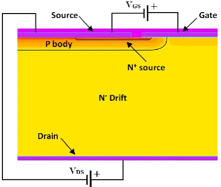
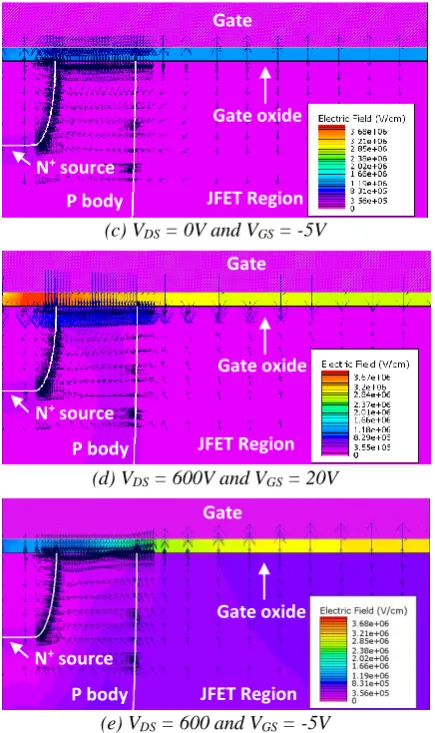
[image:2.595.309.537.115.308.2]The half-cell structure of SiC Planar MOSFET is presented in Fig. 1. Static 2D TCAD physical simulations were carried out in order to show that the electric field (E) distribution near the SiC-SiO2 interface is much higher than in the drift region due to the mismatch in the dielectric constant of the oxide and the semiconductor as explained in the previous section. The simulations for electric field distributions near the SiC/SiO2 interface for various test conditions are illustrated in Fig. 2. As mentioned earlier, having a mismatch between the SiC and SiO2 dielectric constant is another main issue that is restricting device manufacturers to fully exploit the benefits offered by SiC material. Several studies have shown that the SiC devices can also be made with other dielectric materials to further enhance their performance [4, 8].
Fig. 1. SiC MOSFET half-cell planar structure
The electric field distribution inside the gate oxide is very uniform for gate bias stress only as shown in Fig. 2b and 2c. The direction of the electric field would obviously be different depending on the polarity of the gate bias stress as shown. But on the other hand, for drain source bias (VDS = 600V) in Fig. 2a, the electric field is maximum in the centre of the gate oxide and decreases towards the source as expected with decrease in the potential inside the JFET region.
(a) VDS = 600V and VGS = 0V
(b) VDS = 0V and VGS = 20V P body
N+ source
Gate
JFET Region Gate oxide P body
N+ source
Gate
(c) VDS = 0V and VGS = -5V
(d) VDS = 600V and VGS = 20V
[image:3.595.70.288.115.482.2](e) VDS = 600 and VGS = -5V
Fig. 2. Simulation result showing electric field distribution near the SiC/SiO2 interface at different
bias conditions (Zoomed in)
In Fig. 2d, the electric field in the gate oxide is maximum near the N+ source for VDS = 600V and VGS = +20V and it decrease towards the centre of the gate oxide. On the other hand, for VDS = 600V and VGS = -5V, the electric field is the maximum in the middle of the gate oxide and it decreases towards the N+ source as shown in Fig. 2e. It is worth noting that the maximum net electric field in the gate oxide is higher for negative gate bias with drain source bias (Fig. 2e) as compared to the case with just the negative gate stress and no VDS (Fig. 2c). This is because for the earlier case, the direction of electric field produced due to VDS = 600V and VGS = -5V is positive from drain to gate and source to gate respectively. The opposite can be said for Fig. 2d since the direction of electric field due to VGS = 20V and VDS = 600V is
positive from gate to source and positive from drain to gate respectively. Therefore, the net electric field in the centre of gate oxide is smaller.
3. Experimental methodology and test setup
3.1. Stress setup
The test circuit designed is a 2-level 3-phase inverter which is able to include six devices under test (DUTs) at a time. The DUTs are the latest generation commercially available 1200V 36A rated TO-247 packaged SiC MOSFETs from CREE. The schematic of the implemented 3-phase inverter is shown in Fig. 3. The inverter operates without any load in order to be able to observe the change in VTH and IGSS induced purely due to pulsed-gate bias and drain-source bias stress without any current conduction through the DUTs. Current conduction is undesirable as it would not only lead to unnecessarily heat up of devices, but could also have an impact on the monitored parameters. Therefore, to understand the true effect that pulsed-gate bias and the high electric field due to drain-source bias stress has on the VTH and IGSS, DUTs did not conduct any current.
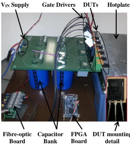
[image:3.595.310.531.530.672.2]Fig. 4 shows the 3-phase inverter test circuit based on the circuit schematic in Fig. 3. A double sided 4 oz copper PCB board was used as a power plane and the gate drivers were vertically mounted onto the power PCB directly without wires in order to avoid voltage overshoot by minimising parasitic inductance. The devices are tightly screw mounted onto the hotplate as shown in the zoom-up (see inset) in Fig. 4.
Fig. 3. Schematic of 3-phase Inverter test circuit with no load
P body N+ source
Gate
JFET Region Gate oxide P body
N+ source
Gate
JFET Region Gate oxide
P body N+ source
Gate
The capacitor bank is rated at 900V to allow (VIN) characterisation up to 900V and the DUTs were mounted horizontally onto the hotplate to allow characterisation at different case temperatures (TCASE) up to 150°C. This is a common setup that is also used for other tests and hence such big capacitors were used.
Fig. 4. 3-phase Inverter test circuit
[image:4.595.312.522.311.683.2]An open loop pulse width modulation (PWM) control was implemented to control the switching sequence of 6 DUTs using an Altera FPGA board. In an ordinary 3-phase inverter, the gate signal of the two switches in one leg should be complementary with an insertion of dead-time between the commutations to avoid any shoot-through as illustrated in Fig. 5. The switching commutation in each leg is also phase-shifted by 120°C but that is not really required here since there is no current conduction.
Fig. 5. Illustration of dead-time
The switching frequency was 10 kHz (50 Hz sine modulating signal and 10 kHz triangular carrier signal) with a dead-time of 400ns and a modulation index of 0.65. Dead-time of 400ns was chosen since the devices are fast to turn ON and OFF with around 100ns of rise and fall time respectively. Modulation index of 0.65 was chosen to represent industrial applications requiring 270V sinusoidal rms output. The applied VGS was switched between +20V and -5V. The illustration of PWM scheme and the gate signal is shown in Fig. 6a and 6b respectively. The carrier frequency in Fig. 6a (illustration purpose only) is much smaller than the actual carrier frequency in the experiment as it is very difficult to show the 10 kHz carrier signal for one period of the 50Hz modulating signal.
(a) Illustration of PWM scheme
[image:4.595.71.296.599.684.2](b) Gate signal
Fig. 6. PWM scheme and resulting gate drive signal
VIN Supply Gate Drivers DUTs Hotplate
FPGA Board Capacitor
Bank Fibre-optic
Board
When the top switch in a leg is ON and the bottom switch is OFF, the bottom switch blocks the full VIN voltage. Once the top switch turns OFF, the bottom switch is still OFF due to the dead-time, the top and bottom switch will each have a blocking voltage of about VIN/2. After the dead-time, the bottom switch will then turn ON and at this time, the top switch stays OFF therefore, the top switch will be blocking the full VIN voltage. The VDS of each device swing between 0 to VIN/2 and VIN/2 to VIN.
3.2. Parameter monitoring setup
The circuit schematics for measuring VTH and IGSS are shown in Fig. 7a and 7b respectively. The VTH was defined as the gate-source voltage at which the ammeter measuring drain current (ID) read 5mA when VDS = VGS. The IGSS was measured at VGS = 20V. For measuring ID and IGSS, Keithley 6485 Picoammeter and 2635A System Sourcemeter, capable of measuring dc current as small as 1pA, were used respectively.
[image:5.595.316.521.178.323.2](a) (b) (b) Fig. 7. Schematic for measuring (a) VTH and (b) IGSS
4. Experimental results and discussion
4.1. High temperature gate bias (HTGB) test
Some results for the HTGB static tests from our previous work (see [7] for more information) on SiC MOSFET reliability of the previous generation CREE devices are included here in Figure 8. The summary of the test results is included in Table 1.
Table 1 Summary of test conditions for HTGB
DUTs VGS
(V)
VDS
(V)
TCASE
(OC)
Duration (hours)
4 +20 0 150 1000
Results for positive gate-bias stress (Fig. 8) show that VTH had a positive shift as the stress duration increased. The main point to be noted here is the huge VTH instability when subjected to HTGB stress.
Fig. 8. High temperature gate-bias (HTGB) Results
4.2. High temperature pulsed-gate switching testing
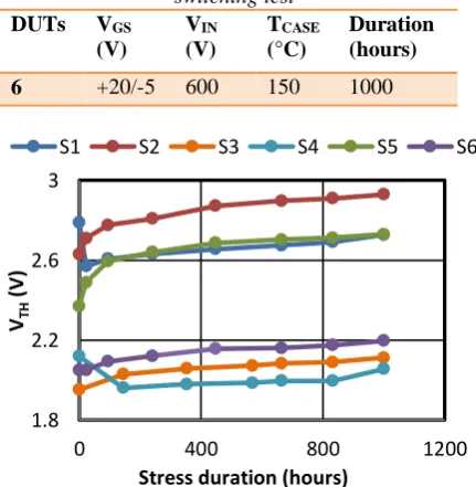
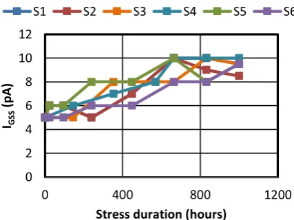
[image:5.595.75.284.377.526.2]The devices were subjected to total stress duration of 1000 hours of bias stress and the VTH and IGSS were measured at regular intervals. The behaviour of VTH and IGSS with respect to stress duration is plotted in Figure 9a and 9b respectively for the test conditions mentioned in Table 2.
Table 2 Summary of test conditions for pulsed-gate switching test
DUTs VGS
(V)
VIN
(V)
TCASE
(°C)
Duration (hours)
6 +20/-5 600 150 1000
(a) Threshold voltage (VTH) evolution
2 3 4 5
0 400 800 1200
VTH
(V)
Stress duration (hours) VGS= +20V
DUT_1 DUT_2 DUT_3 DUT_4
1.8 2.2 2.6 3
0 400 800 1200
VTH
(V)
Stress duration (hours)
[image:5.595.311.527.474.695.2](b) Gate leakage current (IGSS) evolution
Fig. 9. Evolution of monitored parameters; VIN =
600V; VGS = +20/-5; TCASE = 150°C
In Fig. 9a, it can be seen that VTH mainly increases as the duration of stress increases. Initially, the change in VTH is apparent but afterwards as the stress accumulates, VTH seems quite stable with very small change in later values as compared to HTGB results where large VTH instability was seen. The E
distribution simulations clearly indicate that applying VDS and positive VGS bias in fact results in a smaller electric field in the oxide than for the case of positive VGS bias alone (see Fig. 2b and 2d). Whereas on the other hand, the simulations clearly indicate that applying VDS and negative VGS bias in fact results in a higher electric field in the oxide than for the case of negative VGS bias alone (see Fig. 2c and 2e).
When positive gate source voltage (VGS) bias is applied to turn ON the device by forming a channel, the electrons get attracted to the positive gate potential i.e. the SiO2/SiC interface where a small concentration will get injected into the oxide. As mentioned earlier, the SiO2/SiC interface contains traps which are created during the oxidation process. When the electrons move through the oxide layer, a proportion of them get trapped in the interface traps which then leads to negatively charged centers. In order to overcome the additional negative charge due to the trapped negative charge, a larger potential difference i.e. VTH will be required to turn ON the device [4]. The results in Fig. 9a (also in Fig. 8) clearly demonstrate that this physical phenomenon is taking place inside the devices. And the opposite can be said for the negative gate-bias stress since the electrons move out of the traps and hence a lower VTH potential would be required to turn ON the device.
Moreover, another reason of the net positive shift in VTH seen for pulsed-gate bias stress could be due to the modulation index of 0.65 which meant the devices were ON (positive bias at +20V) for 65% and OFF (negative bias at -5V) for 35% of the total stress duration. It would also be interesting to see the VTH evolution if the modulation index is less than 0.5.
Fig. 9b shows the IGSS behavior when subjected to the pulsed-gate stress. It increases slightly in the beginning but towards the end of the stress duration, it seems quite stable. However, no big changes in the IGSS were observed. Due to the nature of the measurement (IGSS), an average value was taken since the measurement is too small and is prone to sensitivity hence the readings fluctuated a lot. Every possible effort was made to have as accurate measurement as possible for IGSS.
5. Conclusion
Pulsed-gate switching bias tests were performed on the latest generation CREE SiC MOSFETs in order to characterise its gate oxide reliability. In order to do that, DUTs were subjected to pulsed-gate bias and drain-source bias stress. The parameters named VTH and IGSS were monitored at regular intervals and the change in these parameters were recorded. The test setup was designed to subject the DUTs to a much more realistic power electronic operating conditions. The results have shown that the change in VTH for pulsed-gate bias stress is much smaller than for HTGB with positive bias. The reason for this is clearly the smaller electric field due to VDS bias.
References
[1] Treu M, Rupp R, Sölkner G. Reliability of SiC power devices and its influence on their commercialization – review, status, and remaining issues. IEEE IRPS; 2010. p. 156–61.
[2] Mawby PA, Kampouris C, Koh A. Advances in silicon carbide MOS technology. In: Proc. 23rd international conference on microelectronics, vol. 1, Nis, Yugoslavia; 12–15 May 2002.
[3] Friedrichs P, Kimoto T, Ley L, Pensl G, “4H-SiC MISFETs with nitrogen-containing insulators,” in Silicon Carbide Volume 2: Power Devices and Sensors, 1st ed. Weinheim, Germany: Wiley-Vch, 2010, ch. 10, sec. 10.2, pp. 237-238
[4] Nawaz M., On the Evaluation of Gate Dielectrics for 4H-SiC Based Power MOSFETs, Active and Passive Electronic Components, Volume 2015, December 2014, Pages 1-12
[5] Green R, Lelis A, habersat D. Application of reliability test standards to SiC power MOSFETs. In: Reliability physics symposium (IRPS). IEEE International; 2011. p. ex.2.1–ex.2.9.
[6] Das, Mrinal K., et al. "SiC MOSFET reliability update." Materials Science Forum. Vol. 717. 2012.
[7] L. Yang, A. Castellazzi, High temperature gate-bias and reverse-bias tests on SiC MOSFETs, Microelectronics Reliability, Volume 53, Issues 9– 11, September–November 2013, Pages 1771-1773.
[8] Robertson J., High dielectric constant oxides, The European physical journal applied physics, March 2004, Pages 265-291.
0 2 4 6 8 10 12
0 400 800 1200
IGS
S
(p
A
)
Stress duration (hours)