warwick.ac.uk/lib-publications
A Thesis Submitted for the Degree of PhD at the University of Warwick Permanent WRAP URL:
http://wrap.warwick.ac.uk/80185
Copyright and reuse:
This thesis is made available online and is protected by original copyright. Please scroll down to view the document itself.
Please refer to the repository record for this item for information to help you to cite it. Our policy information is available from the repository home page.
A Multiple-SIMD Architecture for
Image and Tracking Analysis
Darren James Kerbyson
A Thesis Submitted to the University of Warwick for the degree of
Doctor of Philosophy
Department of Computer Science
University of Warwick
December 1992
" . . ,,~.' ,.'.
Summary
The computational requirements for real-time image based applications are such as to warrant the use of a parallel architecture. Commonly used parallel architectures conform to the classifications of Single Instruction Multiple Data (SIMD), or Multiple Instruction Multiple Data (MIMD). Each class of architecture has its advantages and dis-advantages. For example, SIMD architectures can be used on data-parallel problems, such as the processing of an image. Whereas MIMD architectures are more flexible and better suited to general purpose computing. Both types of processing are typically required for the analysis of the contents of an image.
This thesis describes a novel massively parallel heterogeneous architecture, implemented as the Warwick Pyramid Machine. Both SIMD and MIMD processor types are combined within this architecture. Furthermore, the SIMD array is partitioned, into smaller SIMD sub-arrays, forming a Multiple-SIMD array. Thus, local data parallel, global data parallel, and control parallel processing are supported.
After describing the present options available in the design of massively parallel machines and the nature of the image analysis problem, the architecture of the Warwick Pyramid Machine is described in some detail. The performance of this architecture is then analysed, both in terms of peak available computational power and in terms of representative applications in image analysis and numerical computation. Two tracking applications are also analysed to show the performance of this architecture. In addition, they illustrate the possible partitioning of applications between the SIMD and MIMD processor arrays.
Contents
Summary ... i
1 Introduction ...
11.1 Background ... 1
1.1.1 Image analysis ... 2
1.1.2 Parallel architectures ... 3
1.2 Outline of this Thesis ... 4
2 Parallel
Architectures ... 7
2.1 Intrcxiuction ... 7
2.2 Classification of Parallel Architectures ... 9
2.2.1 Memory Structure ... 10
2.2.1.1 Shared memory ... 10
2.2.1.2 Distributed shared memory ... 11
2.2.1.3 Distributed memory ... 12
2.2.2 Inter-connection networks ... 13
2.2.2.1 Bus based systems ... 13
2.2.2.2 Static interconnection networks ... 14
2.2.2.3 Dynamic interconnection networks ... 17
2.2.3 The control of parallel processors ... 19
2.2.4 SIMD vs. MIMD arrays ... 21
2.2.4.1 Active Resources ... 22
2.2.4.2 Technology ... 23
2.2.4.3 Programming ... 24
2.2.4.4 lA>cal autonomy ... 25
2.3 Survey of Existing Parallel Machines ... 27
2.3.1 SIMD architectures ... 27
2.3.1.1 Bit-serial SIMD processor arrays ... 28
2.3.1.2
Multi-bit SIMD processor arrays ... 332.3.2 MIMD Architectures ... 36
2.3.2.1 Shared Memory machines ... 36
2.3.2.3 Distributed memory ... 39
2.4 Summary- ... 41
3 Architectural Options for Image Analysis ... 43
3.1
Introouction ...
433.2 Image Analysis Processing ... 44
3.2.1 Iconic processing ... 46
3.2.2 Intermediate processing ... 47
3.2.3 Symbolic processing ... 48
3.3 Computational Requirements for Image Analysis ... 48
3.4 Image Analysis Architectures ... 51
3.4.1 Dedicated hardware ... 52
3.4.2 Homogeneous pyramids ... 53
3.4.3 Reconfigurable ... 55
3.4.4 Heterogeneous architectures ... 56
3.5 Summary- ... 60
4 The Warwick Pyramid Machine ... 62
4.1 Intro<:luction ... I t • • • • • • • • • I t • • I t • • • • • • • • • • • • • • • • I t • • • • • I t • • I t • • • • • I t • • I t • • • • • I t • • 62 4.2 Overview of the WPM ... 63
4.3 Implementation of the WPM ... 65
4.3.1 The SIMD array ... 66
4.3.1.1 Functionality of the DAP PE ... 67
4.3.1.2 The SIMD associative Count ... 70
4.3.2 The MIMD array ... 72
4.3.3 The Cluster Controller ... 74
4.3.3.1 The Cluster Bus ... 75
4.3.3.2 The interface between the DAP SIMD array and the controller ... 76
4.3.3.3 The scalar ALU ... 77
4.3.3.4 Instruction sequencing ... 79
4.3.3.5 The shared memory between the controller and the Transputer ... 82
4.3.4 Connecting Clusters together ... 83
4.3.4.1 Communication at the SIMD level ... 84
4.3.4.2 The synchronisation of Clusters ... 86
4.3.5 The prototype system ... 90
4.3.6 M-SIMD Operation of the WPM ... 92
4.4 Programming the WPM ... 93
4.4.1.1 The use of CLASS for Cluster operations ... 96
4.4.2 Remote procedure calls between C and CLASS ... 97
4.4.3 Pyramid C++ ... 99
4.5 Performance of the WPM ... 101
4.6 Summary ... 103
5 Mapping and Processing Data on the WPM M-SIMD Array ... 104
5.1 Introduction ... 104
5.2 The Advantage of M-SIMD over SIMD ... 105
5.2.1 I..ocaIAutonomy ... 105
5.2.2 Associative Response Operations ... 108
5.2.3 Count Response ... 111
5.2.4 Data communication ... 112
5.3 Mapping Data onto the M-SIMD Array ... 113
5.3.1 Sheet mapping ... 114
5.3.2 Crinkled mapping ... 114
5.3.3 Comparison of Data mappings ... 115
5.4 Image Operations on the M-SIMD Array ... 117
5.4.1 SIMD filtering operations ... 117
5.4.2 The use of the WPM associative count ... 121
5.4.2.1 Histogram generation ... 122
5.4.2.2 Rank order filters ... 124
5.4.2.3 Mean and Variance calculation ... 126
5.4.2.4 Image moment calculations ... 127
5.5 Matrix Operations on the WPM ... 128
5.5.1 Mapping considerations ... 129
5.5.2 Matrix Algorithms ... 131
5.5.2.1 Matrix addition and subtraction ... 131
5.5.2.2 Matrix multiplication ... 131
5.5.2.3 Matrix inversion ... 133
5.5.2.4 Mattix trans'pose ...
I t • • • • • • • • • • t . t • • • • • • • • t • •134
5.5.3 Performance of matrix operations ... 1355.5.3.1 Addition and subtraction performance ... 137
5.5.3.2 Multiplication performance ... 138
5.5.3.3 Inversion performance ... . . . .. . .. 141
5.5.3.4 Transpose performance. . . .. . . .. 141
5.6 Summary ... 143
6 The Performance of Tracking Operations on the WPM ...
1456.1.1 Estimation of unknown quantities ... 146
6.2 Tracking Algorithms ... 148
6.2.1 Tracking models ... 150
6.2.2 Data Association ... 154
6.2.2.1 The Nearest Neighbour Standard Filter ... 156
6.2.2.2 The optimal Bayesian approach ... 156
6.2.2.3 The Probabilistic Data Association Filter ... 157
6.3 Tracking Application 1 - Object Tracking ... 159
6.3.1 Object tracking models ... 160
6.3.1.1 Position tracking model. ... 160
6.3.1.2 Size tracking model. ... 161
6.3.2 Object detection and segmentation processing ... 163
6.3.2.1 ObjectDetection ... 164
6.3.2.2 Object Segmentation ... 167
6.4 Tracking Application 2 - Generic Target Tracking ... 170
6.4.1 Image processing operations ... 171
6.4.1.1 Image thresholding ... 171
6.4.1.2 Monotonicity Operator ... 171
6.4.1.3 Corner detection ... 172
6.5 Performance on the WPM ... 174
6.5.1 The image processing ... 174
6.5.2 Tracking operations ... 175
6.5.2.1 The data association ... 176
6.5.2.2 Processing of the Kalman filters ... 178
6.6 Summary ... 182
7 Load-Balancing on the WPM ... 183
7.1 Introduction ... 183
7.2 Minimising Clusters Used for Processing ... 185
7.2.1 Calculation of Image Shifts ... 186
7.2.2 Voting on an image shift.. ... 188
7.3 The Bin Packing of Clusters ... 191
7.3.1 Three-dimensional bin packing ... 192
7.3.2 Two-dimensional bin packing ... 194
7.3.3 Comparison between the FDDH and the FPDS algorithms.. . . ... . .. . . .. . .. . . .. . . .. . .. . . .. . . .. . . .. . . .. . . .. . . .. . . .. 197
7.3.4 Implementation of the load-balancing algorithms ... 200
7.4.2 The Partitioned Monotonic Lagrangian Grid ... 207
7.4.3 Comparison between the MLG and the PMLG ... 209
7.4.4 Construction of an MLG on an SIMD array ... 212
7.5
Summary ...
2138 Conclusions ...
215Bibliography ...
220Appendix A • Cluster Bus Ports ...
234Appendix B • The Cluster Assembler ...
240List of Figures
2.1 A shared memory system ... 11
2.2 A distributed shared memory system ... 11
2.3 A distributed memory system ... 12
2.4 Some static interconnection network topologies ... 15
2.5 Three dynamic interconnection topologies ... 18
2.6 The organisation of an SISD architecture ... 19
2.7 The organisation of an SIMD architecture ... 20
2.8 The organisation of an MISD architecture ... 20
2.9 The organisation of an MIMD architecture ... 21
2.10 The organisation of an M-SIMD architecture ... 26
2.11 The configuration of a two-dimensional SIMD array ... 27
2.12 The MPP processing element ... 29
2.13 Example reconfiguration of the RP A PEs ... 31
2.14 Two CM2 Nodes with associated memory and floating point unit. ... 32
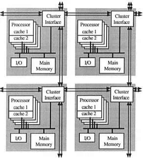
2.15 Four clusters from the DASH prototype ... 38
3.1 Example image analysis processing flow ... 44
3.2 The levels of processing within image analysis ... 46
3.3 The configuration of the SYDAMA-2 system ... 53
3.4 The structure of a multiple-layer homogeneous pyramid architecture ... 54
3.5 The Orthogonal Multi-Processor with an Enhanced mesh ... 57
3.6 The Image Understanding Architecture ... 59
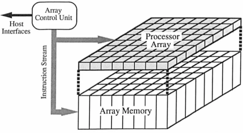
4.1 The Warwick Pyramid Machine ... 63
4.2 A Cluster, the modular component of the WPM ... 64
4.3 A 16x16 DAP SIMD array, showing the detail of 4 PEs ... 66
4.4
The DAP processing element ...
I t • • • • • • • • • • • • • I • • • I t • • • • • • • • • • • • • f • • •67
4.5 A 64 input count ... I t • • • • • I t • • I t • • • • • • • • • • • • • • • • • • • • • • • • • • • • • • I t • • • • • • • • • • • • • • • • • • • • • • • • 71 4.6 A 256 input count from four 64 input counts ... 724.7 The internal components of a T800 and a T9000 Transputer ... 73
4.9 Operation of the Cluster Bus ... 76
4.10 Interface between the SIMD array and the controller ... 77
4.11 The controllers scalar ALU (the AMD29116) ... 78
4.12 The Cluster controllers intruction word ... 80
4.13 The controllers sequencer showing Transputer Load path ... 81
4.14 The shared memory between the Transputer and the controller ... 83
4.15 The interconnection of four Clusters ... 84
4.16 Interconnecting Cluster SIMD arrays ... 85
4.17 The hand-shaking mechanism between Clusters ... 87
4.18 Example synchronisation between six Clusters in a shift operation ... 89
4.19 The prototype Cluster boards ... 91
4.20 The Remote Procedure Call frame used within the Cluster ... 97
5.1 Number of regions that can be processed in parallel on an ideal M-SIMD architecture and on the WPM M-M-SIMD array ... 106
5.2 Efficiency of the WPM and SIMD array for varying region sizes ... 107
5.3 Comparison between the ideal SIMD architecture, the WPM M-SIMD array and an M-SIMD array for associative response operations ... 109
5.4 Relative performance of the WPM M-SIMD array, and an SIMD array, with the ideal M-SIMD architecture for associative operations ... 110
5.5 The time taken to count the number of bits set in a single bit plane on both an SIMD array and on the WPM ... 112
5.6 The time taken to shift data across the M-SIMD array within the WPM, and an SIMD array... 113
5.7 Sheet and Crinkled data mappings on an array processor ... 115
5.8 Convolution paths for a 5x5 mask on an array processor ... 118
5.9 3x3 convolution masks for smoothing and high-pass filtering ... 120
5.10 The horizontal Sobel gradient operator ... 120
5.11 The Sobel operator decomposed into neighbour additions ... 121
5.12 The Faddeev formulation of matrix inversion ... 133
5.13 Example iteration of the Faddeev inversion algorithm on a 3x3 matrix ... 134
5.14 Transposing a matrix on an array processor ... 134
5.15 An example of sixteen matrices mapped onto a processor array ... 136
5.16 Time taken to perform a 16x 16 matrix addition for a varying number of matrices ... I f • • • I f • • • • • • • • • • • • I • • • I • • • • • • • • • • • • • I f • • • • • • • • • • • • • • • • I f • • • • • I f • • • • I • • • • • I t 138 5.17 16x16 matrix multiplication on a 128x128 DAP SIMD array ... 138
5.18 16x 16 matrix multiplication on an 8x8 Cluster WPM ... 139
5.20 Comparison between the WPM and the DAP SIMD array for matrix
multiplication over a range of matrix sizes. . . .. . . .. . . .. . . . .. . . .. . . .. . . .. 140
5.21 Comparison of the minimum time for matrix inversion between the DAP
and WPM arrays ... 141
5.22 Comparison of matrix transpose on the DAP and WPM arrays ... 142
6.1 The combination of two Gaussian measurements ... 147
6.2 Example of validation gating in two dimensions ... 156
6.3 Two images from a sequence approaching a car ... 159
6.4 Processing flow showing image processing, size and position tracking ... 160
6.5 The Imager showing relationship between the size of an object and its depth from a camera ... 161
6.6 Example detection of circles using the circular Hough transform ... 165
6.7 Edge points which contribute to a single parameter space location within the Spoke filter ... 165
6.8 Example of the Spoke filter ... 166
6.9 Example of the Convex hull algorithm ... 169
6.10 Example output from the object segmentation ... 169
6.11 Processing flow in a generic multiple-target tracking environment.. ... 170
6.12 Example image from a meteor sequence ... 171
6.13 The mono tonic operator of Kories ... 172
6.14 Example image showing the categories of the Harris Corner detector ... 173
6.15 The parameters passed between the validation gating, PDAF or NNSF data association and the tracking Kalman fIlters ... 176
6.16 Validation gates mapped onto four Clusters within the WPM ... 177
6.17 Time taken to perform a number of Kalman filter operations, n=4, m=2, on a WPM Cluster and a T800 Transputer ... 180
7.1 The area of an aeroplane on an M-SIMD machine ... 185
7.2 An object across five Clusters showing the possible shift directions that can take place to free each Cluster of it ... 187
7.3 Example of a North-East shift on part of a region mapped across four
Clusters ... , ... 189
7.4 Example distribution of sub-images across the WPM, from four images ... 191
7.5 Example of a set of jobs mapped onto an array processor where each job requires (pj, qj) processors and tj time ... 192
7.6 Example of the malleability of the mapping of sub-images ... 193
7.8 The utilisation of the WPM using the FFDH Shelf and FPDS
load-balancing algorithms ... 197
7.9 The number of sub-images assigned across the WPM using the FFDH Shelf and FPDS algorithms ... 198
7.10 The communications required using the FFDH shelf and FPDS algorithms.. . .. . . ... . . .. . .. . . .. . .. . . .. . . .. . .. . . .. . . .. . . .. .. . . .. . .. . . .. . . .. . . .. 199
7.11 The time cost for the communications required within the FFDH Shelf and FPDS algorithms ... 199
7.12 Example of the MLG mapping on a set of 16 data elements ... 203
7.13 Further example of the MLG mapping resulting in poor locality between data elements ... 204
7.14 Originl vs. MLG separation on randomly distributed data ... 205
7.15 Original vs. PMLG separation on randomly distributed data ... 208
7.16 Mapping nine compressed data sets into a single Cluster ... 209
List of Tables
2.1 Trends in VLSI speed and density ... 8
2.2 Comparison of some network topologies ... 16
4.1 The DAP instruction groups ... 69
4.2 Operations performed for inter-Cluster communications ... 88
4.3 Overhead for synchronised communications ... 90
4.4 Delays across the Cluster bus ... 95
4.5 Comparison of the use of macros and RPC calls ... 99
4.6 Cluster peak computational, memory and communication performances ... 102
5.1 Characteristics of Sheet and Crinkled mappings ... 116
5.2 Time taken for convolution operations on the WPM ... 119
5.3 Comparison of the time taken for the computation of the Sobel filter ... 121
5.4 Comparison of histogram generation algorithms on the WPM ... 123
5.5 Comparison of Rank order filter calculations on the WPM ... 125
5.6 Comparison of the mapping of matrices across a processor array ... 130
5.7 Time for the computation and communication in matrix operations ... 135
5.8 Multiplicative factors applied to the computation, broadcast and shifting times of the various data mappings ... 137
6.1 Image processing operations on the M-SIMD level of the WPM ... 175
6.2 Matrix/vector operations required on a single iteration of a Kalman filter with n states and m measurements ... 179
6.3 Timings for the image processing and tracking operations in the two
tracking applications ... 181
7.1 Voting of the SIMD patches shown in Figure 7.3 ... 190
7.2 Time taken for the load-balancing algorithms ... 201
7.3 Processor operations to find all data points within a distance of 16 pixels
from each oilier ... 212
7.4 Time taken for the construction of a PMLG block on the SIMD array within a WPM Cluster ... 213
Acknowledgements
There are many people to whom grateful thanks are due. Firstly, I would like to thank Professor Graham Nudd, my supervisor, for enabling this work to take place and for his guidance throughout it. I would also like to thank other members of the VLSI group, both past and present, for their help and support. Special thanks must be given to Tim Atherton for his constant enthusiasm to many aspects of this work, and to Roger Packwood for his support in the early stages.
I would also like to thank Tim Atherton and Kay Garbett for their valued work in proof-reading this thesis.
Declaration
This thesis is presented in accordance with the regulations for the degree of Doctor of Philosophy. It has been composed by myself and has not been submitted in any
previous application for any degree. The work described in this thesis has been undertaken by myself except where otherwise stated.
Overviews of the Warwick Pyramid Machine have been published in [Nudd88, Vaudin89, Nudd89, Atherton90, Nudd91, Nudd92a]. The use of the Warwick Pyramid Machine for tracking operations has been published in [Kerbyson92,
Chapter 1
Introduction
1.1 Background
There has been rapid progress in increasing the performance of conventional uni-processor computer systems over recent years [Hennessy90]. Two factors account for much of the performance gained, namely the increase in clock speeds and the increase in the density of components achievable in VLSI. Further, studies of the efficient utilisation of components, within a processor, lead to the development of the Reduced Instruction Set Computer (RISC) approach [Patterson80]. The resulting effect on processors has been an increase in instructional throughput and overall performance.
There are application areas, which have sufficient demands upon computational resources to make uni-processor systems in-feasible options. Parallel processing has become associated with such areas. These application areas include meteorology, oceanography, medical imagery, fuel combustion, and computer vision [Rattner9I]. Current research programmes aim to achieve the processing performances required for these applications, such as that initiated by the
V.S.
government - The Grand Challenges in High Performance Computing [Grand93]. The aim of this is to achieve Tera-Flop (1012 floating point operations) performances for a range of applications.1 Introduction
The factors which increase the amount of computation in image analysis include the spatial resolution of the image sensors, the number of frames processed per second, and the algorithms used. The resolution of the images are increasing, for example, this can be seen with the current shift towards High Definition Television (HDTV) standards [Harris92]. Another factor is the increase in frame rate, e.g. Kodak has recently demonstrated a camera which can capture video at a rate of 1000 frames per second [Kodak90].
Image analysis has received much attention in terms of the algorithms required for specific operations [Suetens92]. However, little work has been done to produce processors able to achieve real-time performance. This thesis is concerned with the computational requirements of image analysis. A major contribution of the work presented here is the analysis of a programmable parallel architecture which has been optimised for use on a range of algorithms found in image analysis.
1.1.1 Image analysis
Image analysis is the process of taking in an image and extracting some high level measurements from it. In a computer vision environment, one would like to use such a system to mimic the functionality of the human visual system. This requires the processing of low-level pixel based information and the processing of high level information after it is extracted from the input images. This processing flow is commonly referred to as a bottom-up approach.
1 Introduction
A generic tracking operation also requires several levels of processing [Kolbe90], as in image analysis. At the lowest level, sensor data is processed to produce possible locations of objects being tracked. These are commonly incorporated into optimal tracking filters, requiring numeric processing on small data sets. Further operations may use the output from the tracking filters for high level decision making processes, such as that for resource allocation.
1.1.2 Parallel architectures
For the efficient utilisation of a parallel machine, the architecture should match the required computation, communication and structure of the data. In image analysis, the computation is such as to warrant a parallel solution. The question remains however, as to which type of architecture is most efficient. Parallel architectures are normally classified into two categories, according to their control structure, either as Single Instruction Multiple Data (SIMD) or Multiple Instruction Multiple Data (MIMD) [Flynn66]. Each type of architecture has their own advantages and disadvantages.
• SIMD architectures are synchronous with each of the processors operating from a single instruction stream [Hord90]. Thus, they act like a sequential processor in that only a single program needs to be written. An SIMD machine can be implemented by the replication of a single processing element. However, a major disadvantage of an SIMD processor is its instruction bottleneck. If the data set being processed, for anyone instruction, is not as large as the SIMD processor array then poor utilisation, and performance, will result. Scaling the size of an SIMD architecture further increases the efficiency problems.
• MIMD architectures do not suffer from the same instruction bottleneck as an SIMD architecture. They enable individual processes to be executed concurrently on each processor. However, due to the asynchronous operation, programming complications can occur such as deadlock. Additionally, the replicated components required for the provision of multiple instruction streams adds to the overall component costs.
1 Introductioo
suited to an SIMD processor array and the higher-level operations are suited to an MIMD processor array. Thus, a heterogeneous architectural solution might be appropriate. That is, a machine which combines some of the features of both SIMD and MIMD architectures.
The main thesis of this work is the analysis of a novel architecture which contains both SIMD and MIMD processor arrays. This machine is termed the Warwick Pyramid Machine (WPM) [Nudd89, Nudd91, Nudd92a, Nudd92b]. It combines a fine grain massively parallel SIMD array, partitioned into smaller Multiple-SIMD arrays, with a course grained MIMD array. This machine was designed from a study of the requirements of image analysis, and is thus aimed at the combined processing of the low and high levels of image analysis.
1.2 Outline of this Thesis
This thesis contains a detailed description of the design and implementation of the Warwick Pyramid Machine. The performance advantages achievable on this architecture are examined. In addition, a number of image processing and tracking operations are examined and the performance analysed on this architecture. Load-balancing techniques, for the efficient utilisation of this architecture, are also described. The thesis is organised in the following way:
Chapter 2 contains a review of parallel architectures. It classifies architectures according to their memory, interconnection and control structures. The ways in which parallel architectures have exploited these factors are described through a review of existing single array machines. The
machines are classified according to their control structure, that is to either
SIMD or MIMD control paradigms.
Chapter 3 reviews the operations involved in image analysis. The computational
requirements of the different processing levels are examined. Architectures, which have been designed to efficiently exploit the different
1 Introduction
Chapter 4 contains a detailed description of the Warwick Pyramid Machine. This machine is a massively parallel heterogeneous architecture combining several processor types. The design of the Warwick Pyramid Machine, the implementation of a prototype, and also the issues concerned with the programming of a dual paradigm architecture, are described.
Chapter 5 contains an analysis of the advantages that this architecture can achieve over conventional parallel architectures. In particular, the capabilities of the Multiple-SIMD array are examined. The mapping of data onto the architecture is illustrated using both image based data and numeric (matrix based) data.
Chapter 6 examines two tracking applications and illustrates how different parts of the processing can be mapped onto the different levels of the Warwick Pyramid Machine. The fIrst is a low density tracking example, from an image analysis application, requiring image operations and the tracking of the size and position of a small number of objects through an image sequence. The second is a higher density situation, treated as a generic target tracking application, where the image pre-processing poses less of a requirement then the actual tracking operations.
Chapter 7 considers the dynamic mapping of data across the Warwick Pyramid Machine, at run-time, to increase the machines utilisation. Load-balancing techniques are considered for both the dynamic mapping of image regions across the machine and for the mapping of sparse data sets.
Chapter 8 draws some conclusions from this work and makes some suggestions for further work.
The contributions to the fIelds of parallel processing and image analysis contained within this thesis include :
1 Introduction
• The novel partitioning of the SIMD array, into a Multiple-SIMD array, within the architecture enabling the instruction bottleneck of conventional SIMD arrays to be overcome. This enables SIMD arrays to be scaled in size without perfonnance inefficiencies.
• The use of the Multiple-SIMD for the novel formulation of some commonly used operations in low-level image analysis.
• The partitioning of tracking applications across the multiple-levels within the Warwick Pyramid Machine.
• The novel formulation of an object size tracking operation that exploits a linear relationship between range and inverse size. This enables a set of size based measurements to be used to estimate the depth of objects from the image plane .
Chapter 2
Parallel Architectures
2.1 Introduction
Applications, such as image analysis and image generation, require vast amounts of computing power if they are to achieve the real-time operation required in robotics and simulation environments. Other areas such as climatic modelling, fluid dynamics, and vehicle dynamics amongst others, also require Tera-Flop (1012 floating point operations) levels of computational power [Rattner91]. The performance of conventional uniprocessor systems cannot currently achieve this level of performance, thus a parallel solution has to be sought.
In this chapter, the options available for the construction of general purpose parallel architectures are described and surveyed. The options include the structure of the memory, the interconnection between processors, and the control structure of multiple processors. The parallel architectures considered here are homogeneous, i.e. those that are constructed from a single type of processor. Later, in Chapter 3, the computational requirements for image analysis are reviewed which leads to a discussion on heterogeneous architectures.
2 Parallel Architectures
ECL CMOS DRAM
Chip level speed (trend p.a.) +20% +20% +12%
Chip density (trend p.a.) +35% +55% +60%
Table 2.1 -Trends in VLSI clock speed and density.
The difference between the trends in the clock rate and the density can be accounted for by the relationship between them and the minimum feature size. The clock speed scales approximately linearly with the minimum feature size, whereas the density scales as the square of it. If the clock speed is solely relied upon to increase present performances, and the current trends continue, then TeraFlop performances will not be achieved within the next 60 years (assuming a current uniprocessor can achieve 30Mflops).
Performance improvements may also be achieved by the use of processors working concurrently, with increasing semiconductor densities as well as increasing the numbers of processors within a system. However it is not usually a simple task to connect together an ever increasing number of processors so that they can co-operate on a single task. In some cases it has been shown that adding more processors into a system can actually increase the amount of time taken for a given task [Hwang85].
Many parallel architectures have been proposed, some have been built and a few have become commercial products. Several surveys on parallel architectures have been carried out, including that of Duncan [Duncan90] which gives an overview of the options available for parallel processing, and those of Gehringer [Gehinger88] and Lim and Binford [Lim87] who survey existing commercial machines. A survey of current (1991) parallel machines, their costs, availability and configurations, is given by Trew and Wilson [Trew91]. In addition, several books are devoted to parallel processing such as that by Hwang [Hwang85] and that by Almasi and Gottlieb [Almasi89].
2 Parallel Architectures
schemes between processors, and control structure. In Section 2.3, existing parallel architectures are described and classified according to their control structures.
2.2 Classification of Parallel Architectures
There are several levels in which a processor can be classed as being parallel. At a high level, a processor may be deemed to be parallel if it belongs to an array of such processors, or at a low level parallelism can be seen through bit-parallel operations within an ALU. Duncan [Ducan90] states that processors which employ only low-level parallel mechanisms should be excluded from any parallel classification and viewed only as sequential processors (often referred to as a von Neumann architecture). Low-level mechanisms within a uniprocessor include:
- Multi-bit (word) operation
- Instruction pipelining, allowing overlapping of various components of a single operations such as fetching, execute, and store
- Separate CPU and I/O capabilities
- Super-scalar, where multiple functional units exist such as in the Motorola 88110 [Diefendorff92]. This contains several integer functional units in addition to separate units for floating point addition, multiplication and division.
However the present generation of Reduced Instruction Set Computers (RISC) have ever increasing functionality, and increased performance in the commercial market place. For instance, the Motorola 88110 includes an additional graphics processing unit with the capability of performing integer addition or subtraction on either 8-, 16-, 32-bit words within its single 64-bit ALU. Each word-length is packed so as to fill the 64-bit ALU. Thus the processing of eight 8-bit data words can take place in parallel within a single cycle. One can see that classifying parallelism is not as simple as it may seem.
2 Parallel Architectures
2.2.1 Memory Structure
An ideal configuration, encompassing both processors and memory, is the Parallel -RAM (P--RAM) model, widely used within theoretical Computer Science, e.g. [Gibbons88]. In this model, it is assumed that a number of processors can simultaneously access any piece of data, from any memory location within the machine, with no overheads or conflicts. Although this is a useful model in the research of parallel algorithms it is not a feasible proposition for implementation. The hardware required to implement n-ported memory increases with the number of processors. In reality, any architecture may be used to simulate a P-RAM model, but with a time penalty due to the control and accessibility of the data within the memory structure.
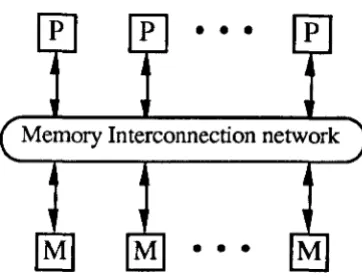
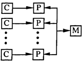
The P-RAM model is feasible, to some extent, when the number of processors in the network is small. This class of machines is commonly referred to as shared memory architectures. In such architectures all processors have access to a common memory structure. An alternative structure, which is somewhat easier to implement, is that of a distributed memory architecture, in which each processor has its own local memory and communicates to other processors or memories through a separate inter-connection network.
2.2.1.1 Shared memory
Shared memory architectures commonly consist of a number of processors connected to a number of memory banks via a switching network - as shown in Figure 2.1. Each processor can simultaneously access all parts of the memory with equal latency. The switching network is responsible for connecting any of the processors to any of the memories.
2 Parallel Architectures
• • •
[image:26.557.215.396.58.197.2] [image:26.557.213.388.569.716.2]• ••
M
Figure
2.1 -A shared memory system.
However as the number of processors increases, the requirements of a memory switching network results in the system being un-economic to implement. In addition, as the number of processors increases, the chances that more than one processor will access the same memory location at anyone time also increases, causing memory contention problems.
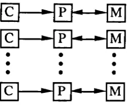
2.2.1.2 Distributed shared memory
In distributed shared memory systems each processor has its own local memory, which may be treated as a cache, and forms part of the overall memory structure. Data which is frequently accessed by the processors is stored within these local memories. Other data can be accessed from the local memories of the other processors, but with increased latency time. The structure of a distributed shared memory system is shown in Figure 2.2.
• • •
•
•
•
Memory Interconnection network
2 Parallel Architectures
The memory network does not need as high a bandwidth as that for shared memory systems since most of the memory access is now between the processors and their local memory. Thus a hierarchical memory system is formed, having a high bandwidth between a processor and its local memory, and a lower bandwidth between a processor and the rest of the shared memory. This system works well as long as the data is efficiently distributed amongst the local memories.
The design of the memory network is not as critical within the distributed system as in the shared memory system since its utilisation is less. This results in a greater potential for scalability with increasing numbers of processors. Problems arise however, when two processors need to process the same data. One solution is to make multiple copies of the data within the processors local memories. This can cause significant cache coherency problems between processors but can be solved for small numbers of processors through a hardware implementation.
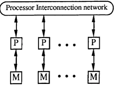
2.2.1.3 Distributed memory
In a distributed memory system, each processor is connected only to its own local memory, with no hardware support for global memory access. Instead the processors themselves are interconnected, allowing data to be passed between processors, using either message passing operations in asynchronous systems (e.g. MIMD) or in lock-step in synchronous systems (e.g. SIMD). The structure of a distributed memory system is shown in Figure 2.3.
Processor Interconnection network
•
• •
[image:27.555.209.398.548.690.2]• •
•
2 Parallel Architeeturcs
The inter-processor network within a distributed processing system is typically slower than that of the two shared memory systems. Thus the distribution of the data, across a network of distributed memory processors, is more critical than within shared memory systems. Message passing, for inter-processor communication in asynchronous systems, has the potential to hide communication latencies by scheduling further processes during the communication time.
Distributed memory systems scale readily. The required communication networks are not as intrinsically inbuilt as those of shared memory systems. The latter places restrictions on the number of processors. The disadvantage of the distributed system is the increase in latency time for the communication of data between processors. This necessitates optimisation of the data distribution so as to minimise the required communications.
2.2.2 Inter-connection networks
The interconnection network between processors in a distributed system, or between memories within shared memory systems, forms an important feature of any parallel architecture. Various interconnection networks have been proposed and generally fall into two categories - static and dynamic [Feng81]. Static networks result in a fixed interconnection scheme and are typically used for inter-processor communication. Dynamic networks have the capability to rearrange the connections between nodes within the network and are used within shared memory systems.
It is advantageous to use a network topology which matches the communication patterns, in the processing of the data, for which the system will be used. However, for a general purpose system, such information about the data can not be assumed in advance. Restricting the system to image processing reduces the available options as will be discussed in Chapter 3.
2.2.2.1 Bus based systems
2 Parallel Architectures
involved. They are easily constructed requiring few resources, growing linearly with the number of processors.
The major disadvantage of a bus based system is that its throughput is fixed. Only one processor communication can take place at anyone time. Thus as the number of processors increases, increasing possible communication traffic, bus contention can become a problem. The effect of this is an increase in average latency times.
2.2.2.2 Static interconnection networks
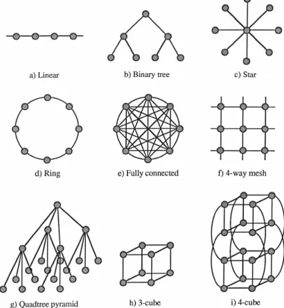
The perfonnance of a bus system can be improved by increasing the number of connections from each processor. The resulting processor topology affects the maximum latency time for communication between two processors. The maximum latency is proportional to the diameter of the processor network (maximum distance between any two processors). Some static interconnection networks are shown in Figure 2.4 and described below. Reviews of interconnection networks have been given by Feng [Feng81] and by Broomell [Broome1l83].
Binary tree - In a binary tree, the maximum number of connections per processor is 3: leaf nodes have 2 and the root has one. Binary trees are particularly useful in supporting divide and conquer algorithms for searching and sorting operations [Duncan90]. Other trees have been suggested but the binary is the most analysed. It is also suited to VLSI implementation. The maximum distance between any two nodes in a binary tree is 210g2(N+ 1) - 2.
Quadtree - The quadtree can be thought of as a two-dimensional binary tree, with several levels of processors, fonning a pyramid and having a single processor on the first level or an apex. Each processor is connected to a single processor in the level above it, and to four processors in the level below it. Additionally the processors can be connected to their four nearest neighbours on the same level. Five connections from each processor are thus required and the maximum distance between any two nodes is 210g2(N+ 1)-2.
2 Parallel Architectures
a) Linear b) Binary tree c) Star
~"" b. ~
~ 'l
~ ~
~
d) Ring e) Fully connected f) 4-way mesh
[image:30.546.89.500.67.512.2]g) Quadtree pyramid h) 3-cube i) 4-cube
Figure 2.4 -Some static interconnection network topologies.
Meshes (ID) - A one dimensional nearest neighbour network forms a single linear
array of processors, each requiring two connections. The maximum distance between any two processors is (N-I) in an N processor system. This distance can
be halved by joining the end two processors together forming a ring topology. Meshes (2D) -Two dimensional processor meshes have been popular in both SIMD
and MIMD processor arrays because of their simplicity and scalability. Typically
2 Parallel Archjtectures
is sometimes referred to as a NEWS (North, East, West, South) network. Other mesh networks have also been implemented: the 6-way mesh which forms a hexagonal grid; and the 8-way mesh in which each processor is also connected to its four nearest diagonal neighbours. The diameter in a 4-way mesh is
2...JN
and in an 8-way mesh is...IN.
These distances can be halved by wrapping around the edges of the array to form a torus network (the top edge connected to the bottom edge and the left edge to the right edge).Hypercube - Each processor within a hypercube requires log2N inter-connections in an N processor system. The maximum distance between any two processors is log2N. The network topology forms a k-dimensional cube (k
=
log2N), three and four dimensional cubes are shown in Figure 2.4. Each processor is addressed by a k-bit binary number. Adjacent processors differ in their addresses by a single bit, determined by which one of the k-dimensions which differs. This leads to simple and elegant communications between processors.Fully connected - Each processor is connected to each other processor in a fully connected network topology. This requires N connections from each processor with a total of !N(N-l) inter-connections in the network for an N processor
network. The implementation of such a network becomes unrealistic for large N.
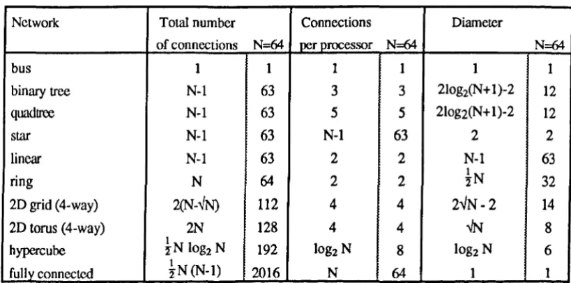
Network Total number Connections Diameter
of connections N=64 per processor N=64 N=64
bus 1 1 1 1 1 1
binary tree N-l 63 3 3 2Iog2(N+l)-2 12
quadtree N-l 63 5 5 21og2(N+ 1)-2 12
star N-l 63 N-l 63 2 2
linear N-l 63 2 2 N-l 63
ring N 64 2 2 !N 32
2D grid (4-way) 2(N-~N) 112 4 4 2~N -2 14
2D torus (4-way) 2N 128 4 4
..IN
81
hypercube ;!N log2 N 192 log2 N 8 log2 N 6
1
fully connected "iN (N-l) 2016 N 64 1 1
[image:31.557.97.507.484.687.2]2 Parallel Architectures
A summary of the connections per processor, the total number of connections within the network, and network diameters is given in Table 2.2 for the networks described above. Also included is an example case for N = 64 processors. The use of the wrap-around on the ID and 2D meshes can be seen be halve the network diameter while having a minimal effect on the total number of connections. The hypercube networks require more inter-connections than the 2D meshes, but their network diameter is proportional to log2N compared with VN for the mesh. The fully connected system requires a large number of connections (proportional to NZ), and in the example case of N = 64, is ten times greater than any other network.
2.2.2.3 Dynamic interconnection networks
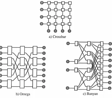
In a dynamic interconnection network, the paths between any two processors is not fixed and connections are made dynamically through the use of switching networks. Their advantage is that the communication paths are set up only when they are required and do not exist permanently. They require less resources than the fully connected static network but potentially have similar communication bandwidths. Such a dynamic network enables each processor to connect with any other processor or, in the case of a shared memory architecture, can be used to connect a processor with any memory bank. Some dynamic crossbar switching networks and multi-stage networks are described below and shown in Figure 2.5.
Crossbar networks
2 Parallel Architectures
a) Crossbar
[image:33.544.126.488.53.369.2]b) Omega c) Banyan
Figure 2.5 -Three dynamic interconnection topologies.
Multi-stage switching networks
The complexity of a crossbar network can be reduced by the use of multi-stage
switching networks. An example is that of the Omega network, Figure 2.5b
[Lawrie75]. Each switching element has four modes of operation: either passing the
inputs straight through; crossing them over; or allowing the upper!lower inputs to be
connected to both outputs. Thus each of the input nodes may be connected to any of
the output nodes. A total of Nlog2N switching elements are required in comparison to
N2 elements in a crossbar. However the latency of the communication has now
increased by a factor of log2N due to the extra switching stages. As the number of
processors increases, the delay across the switching network can become a limiting
factor to the use of multi-stage networks.
A multi-stage network may also be used for connection between differing numbers of
2 Parallel Architectures
number of inputs to each switching element is two while the number of outputs is three, enabling four input nodes to be connected to 9 output nodes.
Multi-stage networks, including that of the Omega and the Banyan, provide nearly as Iowa latency as a common bus system, making them ideally suited to shared memory architectures. However contention can arise in a similar manner to the crossbar network if the desired output path to a node is blocked by a path between other input and output nodes.
2.2.3 The control of parallel processors
A classification of parallel architectures in terms of their control structure was described by Flynn in 1966 [Flynn66]. There have been many more attempts since then for such a parallel architecture classification scheme but only Flynn's has obtained wide spread use. Flynn categorised all architectures into one of four groups:
SISD - Single Instruction Single Data SIMD - Single Instruction Multiple Data MISD - Multiple Instruction Single Data MIMD - Multiple Instruction Multiple Data
These categories are concerned with only two features of an architecture, the number of instruction streams and the number of data streams. The SISD category conforms to a conventional von Neumann architecture which has a single instruction and single data path thus leading to a bottleneck between processor and memories. This is shown in Figure 2.6.
Figure
2.6 -The organisation of an SISD architecture.
The SIMD category again has only a single instructional stream but has multiple data
paths between processors and memory. The processors are required to perform the
2 Parallel Architectures
[image:35.555.236.376.158.268.2] [image:35.555.231.375.495.600.2]bottleneck in the SIMD architectures is not the interface between processors and memory, but is in the single instruction path giving the processors little or no operational autonomy.
Figure 2.7 -The organisation of an SIMD architecture.
The third category, MISD, with multiple instruction streams and only a single data stream is not well defined - how can several operations be performed on the same data at the same time? Flynn suggests that this category suits machines in which either each processor has an instruction stream and all data is stored within a shared memory, or a pipelined machine in which the processors perform their own operations on data which is then passed down a pipeline. The organisation of the MISD architecture is shown in Figure 2.8.
Figure
2.8-The organisation of an MISD architecture.
•
•
•
•
•
•
•
•
•
[image:36.555.243.376.61.170.2]2 Parallel Architectures
Figure
2.9 -The organisation of an M/MD architecture.
In Flynns classification, only two important categories enable parallel processing to take place - namely that of SIMD and MIMD. Both architectures enable operations to take place on multiple pieces of data at anyone time through the provision of multiple data streams and additionally MIMD has multiple instruction streams. A considerable number of parallel machines have been designed, some of which conform to SIMD control and some to MIMD. Several architectures have progressed into commercial products, examples of which are described in Section 2.3.
The majority of the machines which have been implemented have been designed in the form of two-dimensional arrays, although some incorporate a hyper-cube interconnection topology. Array topologies offer scalability in that further processors may be added, forming a larger array, without altering the existing processors to a great extent. One common question which arises in the design of an array is whether the control structure should be SIMD or MIMD?
2.2.4 SIMD vs. MIMD arrays
2 Parallel Architectures
2.2.4.1 Active Resources
A comparison between SIMD and MIMD arrays using a measure of active resources (e.g. gate counts), was given by Uhr in 1982 [Uhr82]. Uhr calculated that 10% of the total gate count in a serial processor (as used in forming Multiple SISD arrays) were active in comparison to 50-66% for an SIMD array. Although the comparison used technologies and machines in existence at that time, the use of active resources to compare architectures remains mostly valid tcxlay.
A comparison made using active resources is only valid if those parts forming the functional units of the processors within the comparison are being fully utilised. This can be viewed at one of two levels: at an operation level where the size of the data effects the utilisation of each processing unit; and at a higher level where the mapping of data elements across the array will effect the overall array utilisation.
An analysis of the utilisation of the functional unit of the processors, when considering different word-length of data, has lead to the conclusion that a set of single-bit processors is more efficient than any other type of processing unit [Hillis85, Uhr82]. Such a processor, commonly termed a single bit Processing Element (PE), can perform any operation that a larger word-length processor can do, but in increased time due to their bit-serial operation.
The utilisation of a processor on different data sizes can be seen through the example of a I-bit and a bit integer addition. A bit addition takes a single cycle on a 32-bit processor, but 32 cycles 32-bit-serially. If it is assumed that 32 bit-serial processors can be implemented using the same amount of resources as a single 32-bit processor then 32 such bit-serial additions can be performed in parallel. A one-bit addition on a 32-bit processor and on a bit-serial processor takes a single cycle to perform. However the bit-serial processors can do 32 such operations in parallel - an improvement by a factor of 32 over the 32-bit processor. In fact, a bit-serial processor may perform an operation on arbitrary sized data with no wastage of cycles.
uni-2 Parallel Architcctures
processor. However a floating point unit within a uniprocessor lies idle on all non-floating point operations. This can lead to poor utilisation of the resources. The resources given to any arithmetic unit, such as a floating point one, may be used to provide an enlarged processor array having an increased performance.
The number of processors within an array is limited, it is affected by the amount of data one wishes to process in a data parallel fashion. This results in a complex trade-off between the number of possible processors in an array and the array utilisation. For instance, if the amount of data to be mapped across the array is less than the number of processors then some processors wil1lie idle, resulting in poor utilisation.
2.2.4.2
TechnologyAnother issue in comparing SIMD and MIMD processing systems is the technology available for VLSI implementation. The numbers of processors which can be implemented within a single IC package are severely limited by the package pin count. The number of components that can be placed on a piece of silicon scales inversely to the square of the feature size. The number of pins on an IC depends upon bonding techniques on the edge of the IC, these have scaled more slowly over the past two decades [Hennessy91]. The package pin-count is of prime importance for a bit-serial processor array where, if it is assumed that memory for each of the processors is implemented using current memory technology off chip, a separate IC pin is required from each bit-serial processor to its memory. Thus the number of pins required scales linearly with the number of processors in the IC.
2 Parallel Architectures
A further technology consideration is the clocking system of the processor array. A bit-serial processor has the potential for a higher clocking rate than a larger grain processor due to the non-existence of carry propagation delays within the processor ALU. However such a clock rate can rarely be achieved if the array uses a large wordlength ALU for its sequencing.
The distribution of the clock can also become a limiting factor in the scaling of an SIMD processor array [Jesshope89]. It becomes increasingly difficult to ensure that all processors will be synchronised, as the array increases in size, due to clock and instruction stream distribution problems. MIMD processors do not suffer in the same way, having both have local clocks and instruction streams.
The possibility of using wafer-scale integration for parallel computers is also being investigated. Wafer-scale integration has been primarily suggested for use in SIMD machines, where the processors may be easily replicated across the silicon, but could be equally be applied to MIMD machines. Example wafer-scale SIMD processors include the WASP bit-serial associative SIMD processor [Lea88], and the 3-dimensional wafer stack from Hughes [Grinberg84]. The use of this technology promises to alleviate any pin-count problems while increasing the density of components in a unit volume.
2.2.4.3 Programming
An MIMD processor array requires the implementation of message passing operations to be used for the communication of data between processors, unless suitable software is available to hide the available parallelism. Problems which may arise from this situation include deadlock.
An SIMD array is considerably easier to program than an MIMD array, acting like a sequential processor in the way in which code is written, requiring only a single instruction stream. To ensure maximum utilisation of the processors, where possible, additional software complexity can arise for the manipulation and mapping of data across an SIMD array.
2 Parallel Architectures
across the array. They can suffer limitations if the operation being performed does not require data parallel computation but instead control parallel computation.
MIMD processor arrays do not suffer the same inefficiencies, in that a data parallel operation may be performed on the MIMD array as if it were a control parallel one, using the message passing operations rather than synchronous communications (Single Program Multiple Data - SPMD operation). However, problems can arise in the debugging of asynchronous programs since the errors can be non-deterministic.
2.2.4.4 Local autonomy
The disadvantage of an SIMD array, and its single instruction stream, may be improved upon by adding local autonomous functions to the processing elements. A discussion on the autonomy options available for PEs was given by Fountain [Fountain88a] along with the cost in terms of percentage increase in hardware complexity. Local autonomy options include:
• Activity control. At its simplest level, this involves a single-bit flag in each PE which indicates if the result of the operations should be written back to memory thus effectively disabling a set of PEs.
• Data control. This enables the address of data within local memory or the local connectivity functions to be calculated locally which otherwise would be calculated globally.
• Function control. This allows the processor to locally control functional units such as barrel shifters or multipliers. This can be useful for the alignment of mantissas in floating point operations.
• Operation control. This provides each PE with a local instruction store, which is sequenced globally, allowing sets of processors to perform different operations.
• Sequencing control. This provides each processor with its own instruction stream thus forming an MIMD processor array, e.g. the Transputer.
The gradual addition of these autonomous functions to an SIMD processor transforms it into an MIMD one. The percentage overhead on the activity, data, function,
2 Parallel Architectures
and between 25-600% respectively. It was assumed that each of the processors contained a 16-bit ALU for this calculation.
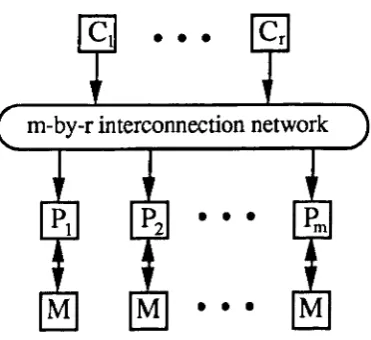
The local autonomy considered by Fountain was limited to the functions that could be added to each individual processor. Maresca [Maresca88] suggests that a more useful and practical level of autonomy is the logical division of processors into clusters, with each cluster having local autonomous control. One example of this is that of a Multiple-SIMD (M-SIMD) architecture which provides local autonomy in the form of instruction sequencing across sets of PEs. This approach has been used in the P ASM processor array [SiegeI81] - a configurable MIMD/SIMD system.
[image:41.555.214.400.413.583.2]A discussion of M-SIMD architectures was given by Hwang [Hwang80, Hwang85]. Hwang used a model containing r PEs which could take their instruction stream from any of m control units using a dynamic reconfigurable switching network as shown in Figure 2.10. On an M-SIMD architecture the resources required for any operation, in terms of PE numbers, can be matched to the amount of data parallelism within it
Figure 2.10 - The organisation of an M-SIMD architecture.
2 Parallel Architectures
2.3 Survey of Existing Parallel Machines
Existing single array parallel machines are described below. They are categorised
according to their control structure, i.e. either to SIMD or MIMO. SIMD architectures
are further classified according to the granularity of their processing elements. Many
SIMD processors have been built using single-bit PEs but more recently incorporate
multiple-bit PEs as a result of the increased integration possible in VLSI. MIMO
architectures are classified according to their memory structure, either shared memory,
distributed shared memory, or distributed memory.
2.3.1 SIMD architectures
The configuration of SIMD machines, designed to date, have been similar and can be
characterised by an array of PEs each with its own memory and controlled by one or
sometimes more array controllers. A characteristic SIMD array is shown in Figure
2.11 where the interconnection scheme is a two-dimensional mesh. The functionality
of the PEs, coupled with their interconnection schemes and the technology in which
they were implemented, gives rise to the performance of each SIMO system.
Host
Interfaces
--I'!!:!I"---Figure
2.11 -The configuration of a two-dimensional SIMD array.
A pioneer project to implement the first large scale SIMD machine, known as ILLIAC
[image:42.545.102.498.436.653.2]2 Parallel Architectures
incorporated 256 64-bit PEs, each with 2Kwords of memory, and a controller for each set of 64 PEs. Each PE had hardware support for floating point operations and could perform a 64-bit multiplication in 400ns. The prototype machine, built in 1972, contained only 64 PEs and was operational from 1975 to 1981. The time lag before the machine became operational was due to the debugging of the hardware, being implemented in the available technology at that time. Each PE used 210 printed circuit boards with the entire machine containing a staggering six million discrete components [Almasi89].
Since the implementation of ILLIAC IV several other SIMD machines have been proposed and built. They can be classified in terms of the granularity of their PEs. Many SIMD arrays use bit-serial PEs, including the Massively Parallel Processor (MPP), the Distributed Array Processor (DAP), the Connection Machine (CM). More recent SIMD designs have used multi-bit processors. These include the Massively Parallel machine (MasPar) and a co-processor to the DAP. The main characteristics of these architectures are described below.
2.3.1.1 Bit-serial SIMD processor arrays.
The Massively Parallel Processor (MPP).
The MPP [Batcher80] was built by Goodyear and was flrst operational in 1983. It is to date one of the largest SIMD processors ever built. It consists of 128x128 PEs forming a two dimensional mesh (or torus with array wrap-around). A single array control unit provides an instruction stream, and also an interface to a host (V AX) computer. Each of the PEs is a simple one bit design with additional functionality, in the form of a shift register, to aid the performance of floating point operations. The MPP processing element is shown in Figure 2.12.
2 Parallel Architectures
shift registers, S, for fast data I/O. Activity control is provided by the G register. Each PE can address 1Kbits of local memory.
A
custom designed le, containing 2x4 PEs, is used to build up the whole MPP array.Shift Register
w
E xternal MemoryFigure
2.12 -The MPP processing element.
More recently, an enhanced version of the MPP processing element has been used within the design of a custom IC. This accommodates 8x16 PEs, using recent technology. The resulting machine has been called BLITZEN, the details of which have been described by Blevins et. al. [Blevins90]. The major differences between the MPP and BLITZEN include 1Kbits per PE on chip, reduced access to off-chip memory (4pins per 16 PEs), 8-way connectivity and an additional local control function of on-chip memory address modification.
The Distributed Array Processor (DAP).
2 Parallel Architectures
The present PE design dates from the mid 70's, having fewer registers per PE. In
1979 four of these PEs could be implemented on a single IC using 200 gate
equivalents [Reddaway79]. The commercial DAP product uses a custom IC containing
an array of SxS of these bit-serial PEs using -3,000 gates. The current DAP machine
consists of an array of either 32x32 or 64x64 PEs.
Each PE consists of a full adder, with 3 inputs and 2 outputs, three general purpose
registers and two multiplexors to route the inputs to, and outputs from, the adder. The
PEs are four way connected in a NEWS communications mesh and also connected to
row and column highways for associative response operations. Additionally the PEs
are connected from South to North for fast autonomous data
I/O.
A PE can address upto 64Kbits of external memory. Each DAP instruction effectively combines the states
of the internal registers with a memory value within a single instruction cycle.
The functionality of the DAP is further explored in Chapter 4.
The CLIP architecture
The Cellular Logic Image Processor (CLIP) series of architectures were designed and
built by Fountain and Duff at University College London. The design of the CLIP-4
processor took place over the ten years to 1980 and is described by Fountain
[Fountain87]. The prototype CLIP-4 consisted of a 96x96 processor array containing
bit-serial PEs like the DAP and MPP. A commercial product consisting of a 32x32 PE
array was also marketed.
Each CLIP-4 PE contained 4 registers, on-chip 32-bit memory, and a Boolean
functional unit able to perform any logical combination on two single bit operand
inputs. A network of adders was included in the CLIP-4 array to generate the sum of
the number of bits set in a binary image. The PEs were arranged in an eight connected
two-dimensional network. Eight PEs were implemented on a single custom
IC.
The Reconfigurable Processor Array (RPA)
The RPA was designed by Jesshope et. a1. [JesshopeS7J at Southampton University.
The goal of the RP A was not to improve the peak computational power of each PE but