Faculty of Electrical Engineering,
Mathematics & Computer Science
Analysis Of
Sub-Sampling Phase-Locked Loop
Dynamic Behaviour
MSc. Thesis M.J.M. Wenting
November 2015
1. Introduction 1
1.1. Phase-Locked Loops . . . 2
1.2. Research Questions . . . 4
1.3. Thesis Outline . . . 4
2. Phase-Locked Loop 5 2.1. Phase-Locked Loop Phase Domain Model . . . 7
2.2. Phase-Locked Loop Figure-Of-Merit . . . 8
2.3. Sub-Sampling Phase-Locked Loop . . . 9
2.3.1. Sub-Sampling Phase-Locked Loop Phase Domain Model . . . 11
2.3.2. Research Questions About the Sub-Sampling Phase-Locked Loop . 13 3. Channel Switching Simulations of a Sub-Sampling Phase-Locked Loop 15 3.1. Simulation Model . . . 16
3.1.1. Design of the Loop Filter . . . 17
3.2. Channel Switching simulations . . . 23
3.2.1. Channel Switching Simulation Setup . . . 24
3.2.2. Channel Switching Simulation Results and Discussion . . . 29
3.2.3. Preliminary Conclusion About the Channel Switching Simulations 34 3.3. Loop Gain Ratio Analysis . . . 35
3.3.1. Loop Gain Ratio Boundary for a linear PFD without a Dead Zone 37 3.3.2. A Linear Phase-Frequency Detector with Dead Zone of Tref/2 . . 38
3.3.3. Loop Gain Ratio Boundary for a linear PFD with a Dead Zone . . 40
3.3.4. Loop Gain Ratio Boundary for a binary PFD with a Dead Zone . 44 3.3.5. Summary of the Loop Gain Ratio Analysis . . . 48
3.4. Channel Switching Simulations - Continued . . . 49
3.4.1. Channel Switching Simulation Setup - Continued . . . 49
3.4.2. Channel Switching Simulation Results and Discussion - Continued 51 3.4.3. Comparison of the Channel Switching Simulation Results . . . 58
3.5. Conclusion About the Channel Switching Simulations . . . 59
4. Lock Perturbation Simulations of a Sub-Sampling Phase-Locked Loop 61 4.1. Lock Perturbation Simulation Setup . . . 61
4.1.1. Expectations for the Simulations . . . 62
4.1.2. Simulation Setup Variables Table . . . 62
4.2. Lock Perturbation Simulation Results . . . 63 4.2.1. Phase-Frequency Detector Without a Dead Zone . . . 63 4.2.2. Linear Phase-Frequency Detector With a Dead Zone of Tvco/2 . . 65
4.2.3. Linear Phase-Frequency Detector With a Dead Zone of Tref/2 . . 65
4.2.4. Binary Phase-Frequency Detector With a Dead Zone of Tvco/2 . . 66
4.2.5. Binary Phase-Frequency Detector With a Dead Zone of Tref/2 . . 67
4.3. Comparison of the Lock Perturbation Simulation Results . . . 69 4.4. Conclusion About the Lock Perturbation Simulations . . . 70
5. Thesis Conclusion 73
5.1. Recommendations for Future Work . . . 76
A. Matlab Simulation Script 77
Since the beginning of civilisation timekeeping has been essential for its functioning. Working together is not very productive if one person turns up a year after the other.
The notion of when something should happen is also very important in electronics. The periodic signal that is used for this timing reference is either called a clock signal or Local Oscillator (LO). Digital circuits rely on this clock to time when an operation is done and the next one can begin. Analog circuits like a mixer, can use an LO to select which channel to receive.
Because the function of the circuit relies on this timing, the accuracy of the timing signal partly determines the circuit’s performance. In the field of frequency synthesis jitter or phase noise gravely impact that accuracy. Jitter being the time deviation of the zero-crossings of the timing signal, as compared to an ideal version of that timing signal. Phase noise is the frequency domain equivalent of jitter. Both therefore, say something about the accuracy of the zero-crossings of the timing signal.
But, as is often the case in electronics there are many circuit parameters as can be seen in figure 1.1, each representing a possible performance metric. Depending on the application a different parameter can be the performance limiting factor.
In the case of Phase-Locked Loops (PLL) there is usually a focus on jitter and power consumption parameters.
For instance, when using a PLL for the clock in a digital circuit it should have low jitter to allow for high speed operation. It should also consume little power so that it can last
longer on a battery.
However, if a PLL is used to select the channel for a radio application like Bluetooth it also important how fast it can change its output frequency. Bluetooth may change its channel 1600 times per second meaning it stays tuned to one frequency for only 625µs. In order to have as much time as possible to send data the channel switching time of the PLL must be much shorter than 625µs [1]. That means the required channel switching time is in the order of 10µs.
1.1. Phase-Locked Loops
The previous section explained that there is a need for an electronic timing signal and that applications can have performance requirements for any circuit parameter. Now it is time to take a closer look at the most employed synthesizer timing signal architecture, called the Phase-Locked Loop (PLL). A basic schematic for a PLL is shown in figure 1.2. A PLL can either be used to synchronize its output frequency with its input frequency or to synthesize a new output frequency from a fixed frequency source. This thesis focusses on using a PLL as a frequency synthesizer.
Reference Frequency
Phase-Frequency
Detector
Charge Pump
Loop Filter
Voltage Controlled
Oscillator
Frequency Divider
Figure 1.2.: Block schematic for a basic PLL.
In the case of frequency synthesis the ”reference frequency” from figure 1.2 comes from a high fidelity timing reference. Commonly used as this reference are piezoelectric mate-rials. Usually these are quartz crystals and have therefore come to be known as crystal oscillators (XO). The jitter of an XO can be very low at for example 124.9 fs when in-tegrated from 100 Hz to 200 kHz [2]. The absolute frequency accuracy of an XO is also very good and usually in the order of 10 to 50 ppm [2]. The biggest down side of using crystals without a PLL is that the available output frequencies are only up to tens-of-megahertz and without the PLL cannot be changed over a wide range.
Firstly, for modern day applications these frequencies are quite low, as applications using frequencies of multiple gigahertz are commonplace. Secondly, most applications that use a timing signal no longer operate on just one frequency, like radio-frequent communica-tion, analog-to-digital converters and digital circuits. Instead, mixers switch frequencies to select a different channel and digital circuits vary their clock frequency to conserve
power.
Thus, an XO is a good reference to start from. However, a functional block in series is needed that converts the high fidelity signal from the XO into a tunable high output frequency. This functional block is either called a Clock Multiplier Unit, Frequency Synthesizer or Frequency Multiplier depending on whether the output signal is used as a time or frequency reference.
There are various known frequency synthesizer architectures of which the most important ones are outlined in [3, Chapter 1.3]. That thesis builds the case for the Phase-Locked Loop (PLL) as being the best choice for a high-speed low jitter frequency synthesizer.
Looking at PLL publications, more often than not the jitter and power consumption are the key performance metrics and therefore focus of the publication. In order to objectively compare PLL implementations with respect to jitter and power consumption, a Figure-Of-Merit (FOM) was derived in [4]. This FOM indicates how far from ideal a PLL is with respect to jitter versus power dissipation. A lower FOM indicates a better design.
Currently, the lowest published FOM is held by the Sub-Sampling Phase-Locked Loop (SSPLL) developed by Gao et al. [5] at the Integrated Circuit Design group of the University of Twente.
However, jitter and power dissipation are only two of many performance measures. For example tunability, is an area where the SSPLL could be improved. A big downside of the traditional PLL is that the output frequency is always stepped by an integer multiple of the reference frequency. These PLLs are therefore called integer-N PLL. The SSPLL in [5] is also of this type.
For instance, this integer stepping of the output frequency directly determines how close adjacent channels can be in a communication link. In modern communication links many closely spaced channels are used to increase the link capacity. To build such a link using an integer-N PLL would require a very low reference frequency to match the channel spacing. For instance, in the GSM-900 standard the channels are spaced only 200 kHz apart [6]. The reference frequency is usually at least ten times higher than the loop bandwidth. This results in a trade-off between channel spacing and the switching time between channels, which is proportional to the loop bandwidth.
To break this trade-off fractional-N PLLs were introduced. A fractional-N PLL can also have an output frequency in between the usual integer steps. A very innovative method to make a fractional-N SSPLL was published in [7].
practical applications.
1.2. Research Questions
The paper by Hsu et al. [8] opened up an internal discussion around the topic of SSPLL dynamic behaviour. Furthermore, in the recommendations of the PhD thesis by Gao [10] a related comment is found: ”In some applications, the PLL settling time is an important specification. In the current design, a classical PLL with dead zone function as the FLL. Having a dead zone during frequency acquisition slows down the PLL settling, which may be problematic. It is worthwhile to investigate the settling behaviour of the SSPLL further.”
The discussion and newly found information led to the following research questions:
> What is the influence of the dead zone in the phase frequency detector on the sub-sampling phase-locked loop dynamic behaviour?
> Can the robustness to perturbations of the SSPLL design from [9] be improved without removing the dead zone in the phase frequency detector?
> Can the dynamic behaviour of the SSPLL design from [9] be improved by optimiz-ing its configuration?
1.3. Thesis Outline
Before going deeper into the analysis of SSPLL dynamic behaviour some general in-formation about PLLs and specifically SSPLLs will be presented in chapter two. The chapter closes with a discussion of some issues of SSPLLs.
Chapter three and four focus on finding answers to the research questions of the SSPLL design. Chapter three starts with loop filter design and loop stability. After that come simulations and analysis related to channel switching. Chapter four continues the simu-lations, but focusses on lock perturbation instead. The results from these two chapters are used to answer the research questions.
The thesis ends with a summary of the important conclusions from the thesis followed by recommendations for future work.
This chapter will briefly describe some concepts concerning Phase-Locked loops (PLL) in general. Later on about the specific implementation called Sub-Sampling Phase-Locked Loop (SSPLL) that is the subject of this thesis will be discussed.
The simplest way of describing a PLL to an electrical engineer is by saying it is a voltage buffer for the phase domain. Like a voltage buffer a PLL is a feedback loop, where the output tracks the input. However, the quantity of interest is the phase of the signal instead of the voltage. By setting the feedback ratio the relation between the in and output of the loop can be defined. When moving on to study the inner working of a PLL things become more tricky. Depending on the node under inspection the quantity of interest may change from phase to current, voltage or frequency. Despite being difficult to analyse, many have studied and written about the PLL because of its usefulness in electronics. An important application for PLLs is as a frequency synthesizer, which is also the focus of this thesis.
The basic buildings blocks for a PLL are shown in figure 2.1. The reference frequency is usually a crystal oscillator (XO) whose jitter can be very low at for example 124.9 fs when integrated from 100 Hz to 200 kHz [2]. The absolute frequency accuracy of an XO is also very good and usually in the order of 10 to 50 ppm [2]. The biggest down side of using crystals without a PLL is that the available output frequencies are only up to tens-of-megahertz and cannot be changed over a wide range. The application area for PLL frequency synthesizers is very wide from the audio range all the way to the gigahertz range.
The Phase Frequency Detector (PFD) modulates the width of its output current as a measure for the phase difference between the reference and the divided VCO output. The Charge Pump (CP) converts this voltage to a current to be fed into the loop filter and theoretically provides infinite gain. The total charge going into the loop filter is called a charge packet and is expressed by ICP ∗Ton. Where Ton denotes the on time of the
charge pump transconductance and adds a degree of freedom for possible gain control. A schematic of the PFD followed by a charge pump and its characteristic are shown in figure 2.2. The PFD-CP characteristic shows a linear relation between the average output current iCP on the y-axis and the phase difference between the reference and the
divided VCO output ∆φdiv on the x-axis. At a phase difference of 2πthe average output
negative for all negative phase differences. This property gives the PFD its frequency discrimination ability. The sign continuity means that the loop control action for a certain frequency difference is always in the same direction. If the characteristic would have additional zero-crossings, the loop control action would also be zero for multiple points. That would mean that there are multiple frequencies on which the PLL could lock. One of the things that makes PLLs useful is the ability to uniquely control the output frequency. Having multiple lock frequencies would mean a loss of this ability. The loop filter suppresses high frequencies and gives the necessary degrees of freedom to stabilise the loop. Together with the PFD and CP an integrator is formed. This is important for the steady-state phase error, which will be discussed in section 2.1. The Voltage Controlled Oscillator (VCO) is a tunable frequency synthesizer that can provide the desired gigahertz output range.
The frequency divider scales the output frequency by a factor N and in doing so sets the relation between the in and output frequency by the same factor.
The most common way to work with a PLL is to use a phase domain model which is presented in the next section.
Reference Frequency
Phase-Frequency
Detector
Charge Pump
Loop Filter
Voltage Controlled
Oscillator
Frequency Divider
Figure 2.1.: Block schematic for a basic PLL.
Figure 2.2.: Schematic of phase-frequency detector and charge pump and its character-istic. [9]
2.1. Phase-Locked Loop Phase Domain Model
PLLs are nonlinear, time-discrete circuits and are difficult to analyse and describe with mathematics. Therefore, a linear time-continuous model is often used and is competent provided that the loop bandwidth is much smaller than the reference frequency which acts as the sample frequency for the PFD. The rule of thumb for PLL design is that the loop bandwidth is at least ten times smaller than the reference frequency in order for the continuous time approximation to be good enough [11].
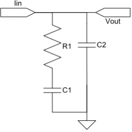
Figure 2.4 shows the phase domain model for a PLL. Most PLLs use a loop filter like the one shown in figure 2.3. This reduces the VCO output phase noise by adding extra suppression for high frequencies on the voltage that tunes the VCO (Vtune). The
trans-impedance of this filter is given by:
Zlf(s) =
Vout
Iin
= 1 C2
· (s+
1
R1C1)
s(s+R1C1C2C1+C2 ) (2.1)
Equation 2.1 shows that the filter has two poles and one zero. In the phase domain the VCO is modelled as Kvco/sas is shown in figure 2.4. This PLL is therefore a third
order system, which is difficult to work with. However, this third order system can be approximated by a second order, by placing one pole at a much higher frequency than the others. This is done by making the second filter capacitance C2 much smaller than
the first. By doing this approximation the system is very similar to a standard second order system from control theory. In section 3.1 the loop filter and loop stability will be discussed further.
By doing the second order approximation the following equations describe the PLL transfer function:
H(s) =N 2ξωns+ω
2
n
s2+ 2ξω
ns+ωn2
(2.2)
wn=
s
KpdKvco
C1N
(2.3)
ξ = R1 2
r
KpdKvcoC1
N (2.4)
Kpf d =
Icp
2π (2.5)
WhereN is the feedback frequency division factor,ξ the damping factor,ωnthe natural
frequency, Kvco the VCO tuning gain, Kpf d the PFD gain and Icp the charge pump
2.2. Phase-Locked Loop Figure-Of-Merit
When working on improving PLLs it is convenient to have a performance number with which to compare if progress has been made. For many circuits an equation for such a number exists. Often the number is called the Figure-Of Merit (FOM). Even though there are many possible measures of quality as was indicated in the introduction by figure 1.1, there are two that are most used for PLLs when trying to quantify performance. The first is the VCO output phase noise or jitter variance when viewed in the time domain. The second is the PLL power consumption.
In a paper by Gao et al. [4] the most used FOM for PLLs is derived:
F OMP LL = 10·log10((
σt,P LL
1s )
2·PP LL
1mW) (2.6)
Whereσt,P LL is the PLL output jitter and PP LL is the total PLL power consumption.
The FOM increases with more power consumption and more output jitter. Because the goal is to create a PLL with as little power consumption and output jitter as possible, a lower FOM indicates a better PLL design.
Figure 2.3.: The schematic for the two pole, one zero loop filter.
φref Kpfd Zlf(s) Kvco/s
1/N
[image:12.595.263.393.357.487.2]φout
Figure 2.4.: The phase domain model of a PLL.
The derivation begins by analysing the propagation of noise sources through a typical PLL phase domain model such as in figure 2.2. From this an optimal PLL loop band-width is derived. The choice of PLL loop bandband-width minimizes the total PLL output phase noise when the phase noise contributions from the reference and loop equal that of the VCO. This also means that the loop and the VCO should be given an equal power budget.
The paper then goes on to show that the in and output frequency have no influence on the output jitter variance.
Lastly, if the assumption is made that all power consumption is dynamic power then it can be shown that the PLL output jitter variance is inversely proportional to the power consumption.
2.3. Sub-Sampling Phase-Locked Loop
With the goal of obtaining the lowest possible FOM, a PLL should have as little output jitter as possible while consuming as little power as possible.
Often the dominating noise source from the loop is the charge pump. If a feedback gain βCP is defined from the PLL output to the charge pump output, it can be shown that
the charge pump noise is suppressed by the square of this gain [9]:
Lin−band,CP ≈
SiCP,n
2βCP2 (2.7)
WhereLin−band,CP is the single side-band noise power to carrier power ratio andSiCP,n
the power spectral density of the charge pump current noise.
To obtain a low FOM the feedback gain should be increased with no additional power consumption.
This is the basis for using a different kind of phase detector with a higher gain instead of the traditional PFD. The Sub-Sampling Phase Detector (SSPD) shown in figure 2.5 is exactly that. The difference with the traditional PFD shown in figure 2.2 is that the SSPD directly samples the VCO output every reference period and outputs a voltage proportional to the phase difference between the reference and the VCO. This is illus-trated in the SSPLL block schematic shown in figure 2.6.
Combined with a charge pump this gives the characteristic shown in figure 2.5. The characteristic shows a sinusoidal relation of the phase difference between the reference and the VCO ∆φV CO and the average output current iCP. The maximum average
out-put current is reached at a phase difference ofπ/2 modulo 2π. In contrast to the PFD, the SSPD characteristic has multiple zero-crossings. This means that the SSPD is not able to discriminate between different frequencies like the PFD can.
gain. In [9] the feedback gain for the traditional PFD and SSPD are given by:
βCP,P F D=
ICP
2πN (2.8)
βCP,SS =AV CO·
2ICP
Vgs,ef f
(2.9)
The equation for the ratio of the VCO output to PD output gain between a traditional PFD and SSPD is therefore given by:
βCP,SS
βCP,P F D
= 4π·N · AV CO
Vgs,ef f
(2.10)
WhereN = fvco
fref,AV COis the VCO output amplitude,Vgs,ef f is the effective gate-source
voltage of the MOS transistor. This ratio is much larger than 1, because 4π,N ≥1 and usuallyAV CO> Vgs,ef f. Therefore the SSPD offers more charge pump noise suppression
than a traditional PFD, resulting in a higher FOM.
Figure 2.5.: Schematic of a sub-sampling phase detector and charge pump and its char-acteristic. [9]
One downside to using an SSPD is that it is frequency agnostic meaning it does distin-guish between samplingN·fref, (N+ 1)·fref or any other multiple. The way this was
solved in [9] was to include a second loop that provides the frequency locking. This sec-ond loop was a traditional PLL with a Dead-Zone (DZ) added to the PFD. This enables the SSPLL to lock to the correct frequency. After that lock is made the traditional PFD is in its DZ and does not contribute to the phase noise.
Lastly, the feedback gain of the SSPD can actually be too high. Section 3.1 will explain that a higher feedback gain requires a larger loop filter capacitance for loop stability. The feedback gain should just be high enough to make the charge pump noise negligible. If the feedback gain becomes higher than that point, the loop filter capacitance must become very large for loop stability without gaining any noise benefit. The feedback
gain can then be said to be unnecessarily high and should be reduced. In [9] this was done by adding a Pulser block that only turns on the charge pump for a fractionτpul of
the sampling period Tref. This reduces the feedback by a factor τpul
Tref. The gain reduced
feedback gain is given by:
βCP,SS=AV CO·
2ICP
Vgs,ef f
· τpul
Tref
(2.11)
The combined structure of sub-sampling and frequency loop is called a Sub-Sampling Phase-Locked Loop. A schematic of an SSPLL is shown in figure 2.6.
Reference Frequency Phase-Frequency Detector Charge Pump Loop Filter Voltage Controlled Oscillator Frequency Divider Dead Zone Charge Pump Sub-Sampling Phase Detector Pulser + + fout Vtune Icp fvco fdiv fref fref fref fvco ISSPD IPFD VSSPD VPFD Sub-Sampling Loop Frequency Loop
Figure 2.6.: Block schematic of an SSPLL.
2.3.1. Sub-Sampling Phase-Locked Loop Phase Domain Model
are simply superimposed to obtain the following transfer function:
H(s) =N 2ξωns+ω
2
n
s2+ 2ξω
ns+ωn2
(2.12)
wn=
s
(βpf d+βsspd)Kvco
C1
(2.13)
ξ = R1 2
q
(βpf d+βsspd)KvcoC1 (2.14)
βpf d =
Kpf d
N =
Icp
2πN (2.15)
βsspd=Ksspd=Avco
2Icp
Vod
· τpul
Tref
(2.16)
WhereN is the feedback frequency division factor,ξ the damping factor,ωnthe natural
frequency, Kvco the VCO tuning gain, βpf d the PFD gain, βsspd the SSPD gain, Icp
the charge pump current,Avco the VCO amplitude andVod the SSPD transconductance
overdrive voltage.
Because this is a linearised model the DZ is not taken into account. The DZ could be added by makingβpf d dependent on the phase difference between the reference and the
divided VCO output. The PFD feedback gain would then be as equation 2.8 for phase differences outside the DZ and zero for phase differences inside the DZ.
φref
Kpfd
Zlf(s) Kvco/s
Ksspd + + 1/N N + -+ φout Sub-Sampling Loop Frequency Loop
Figure 2.7.: The phase domain model of an SSPLL.
2.3.2. Research Questions About the Sub-Sampling Phase-Locked Loop
The original publication of the SSPLL in [9] reported the lowest PLL FOM at the time. Since then there have been many follow up designs all reporting very low FOMs.
A paper by Hsu et al. [8] suggests that the relock time after a disturbance of the SSPLL could use some improvement, because it ”may not be acceptable in many clock synthesis applications”. The paper suggest that the relock time after a disturbance of a PLL needs to be in the order of 1µs though it never mentions a specific target. In one example the SSPLL took 2.5µs to regain lock where a traditional PFD took 0.4µs.
In the recommendations of the PhD thesis by Gao [10] a similar comment is found: ”In some applications, the PLL settling time is an important specification. In the current design, a classical PLL with dead zone function as the FLL. Having a dead zone during frequency acquisition slows down the PLL settling, which may be problematic. It is worthwhile to investigate the settling behavior of the SSPLL further.”
Combined with an internal discussion at the beginning of this thesis the following ques-tions where raised:
> What is the influence of the dead zone in the phase frequency detector on the sub-sampling phase-locked loop dynamic behaviour?
Specifically, in the event of channel switching or lock perturbation the size of the DZ could influence the PLL settling time.
> Can the robustness to perturbations of the SSPLL design from [9] be improved without removing the dead zone in the phase frequency detector?
The big advantage of the original SSPLL was its high phase detector gain and therefore low output noise. By removing the PFD DZ the SSPLL robustness is improved at the cost of mitigating the noise advantage.
> Can the dynamic behaviour of the SSPLL design from [9] be improved by optimiz-ing its configuration?
Sub-Sampling Phase-Locked Loop
This thesis started by explaining the growing interest in the Sub-Sampling Phase-Locked Loop (SSPLL) dynamic behaviour, because of its crucial role in practical applications. Specifically, a paper published by Hsu et. al. [8] raised the issue of the SSPLL’s ro-bustness to perturbations. The proposed solution was to remove the Phase-Frequency Detector (PFD) Dead Zone (DZ) present in the original design from [9]. However, re-moving the PFD DZ mitigates a large part of the noise benefits that the original SSPLL presented.
In this chapter the goal is to find out more about the dynamic behaviour of SSPLLs through simulation and analysis. The insight gained could lead to an SSPLL imple-mentation that keeps all the noise benefits of the original design, but is also robust to perturbations.
The dynamic behaviour of the SSPLL will be examined in two practically relevant situ-ations:
1. Channel Switching: the output frequency of an SSPLL can be electronically set by changing the feedback division ratio. If the SSPLL was previously locked on a different ratio the output is made to switch from one frequency to another, or one channel to another and it is called channel switching. As was illustrated with a bluetooth example in chapter 1 a PLL that can quickly switch between channels can be very useful.
2. Lock Perturbation: If any charge is injected into a phase-locked SSPLL that causes a loss of that lock, it is called lock perturbation. In case a perturbation is large enough to force the SSPLL out of lock it is of interest to know how fast the SSPLL is able to regain lock so that normal operation of integrated circuit can be resumed.
The reason for using simulations as a research tool instead of trying a fully analytical approach is that PLLs are non-linear time-discrete circuits and therefore difficult to handle mathematically. However, as presented in chapter 2 some approximations can be made to get a linear (SS)PLL model that can for instance be used in the lock situation alongside the simulations to gain insight.
cover the first channel switching simulations after which section 3.3 will present new analysis based on insight gained from [8] and the first simulations. Section 3.4 will present adjusted channel switching simulations, because of the new insight from section 3.3. There will be intermediate conclusions and the chapter will close with an overall conclusion.
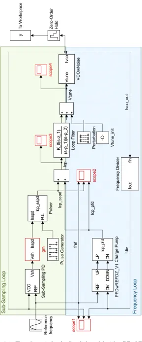
3.1. Simulation Model
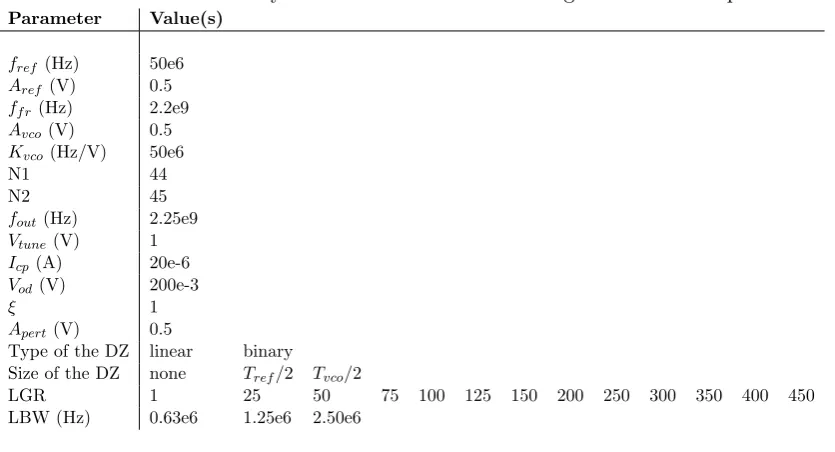
In order to find relations between the settling time, Loop BandWidth (LBW) and Loop Gain Ratio (LGR) a Simulink model of a PLL was created. The schematic of the model is shown in figure 3.1. It has been designed to be representative of the design published in [9]. The parameters are set by the script found in appendix A.
The following list clarifies the function of each block in the model:
> The “Reference” block represents the crystal oscillator source and outputs a sine wave with frequency fref and amplitudeAref.
> The “SubSampling PD” block is a simple sample and hold function that samples “VCO” at the rising edge of “REF”.
> The “gm” block is a transconductance equal to the gm.
> The “Pulser” is a block that only passes its Icp input when PUL is high.
> The “Pulse Generator” makes pulses with a width equal to τpul
Tref everyTref seconds.
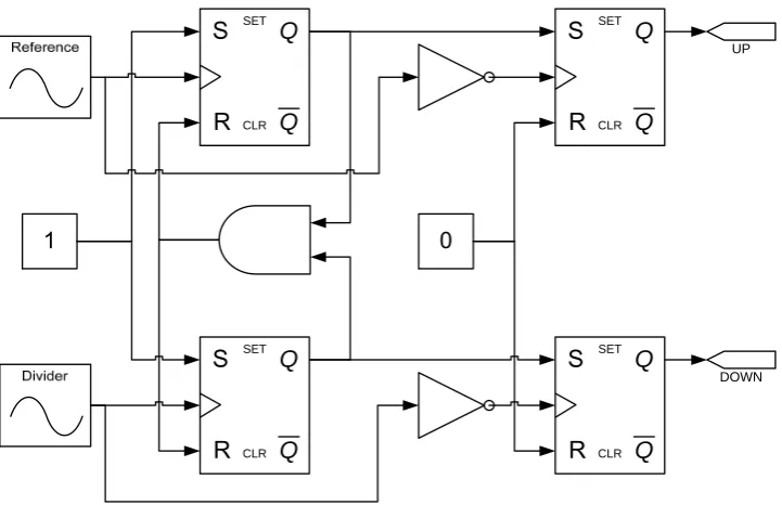
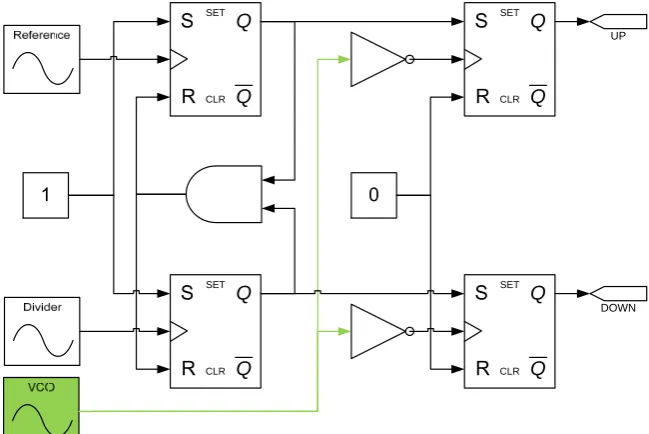
> The block “PFDwDZTrefo2 V1” is a Phase-Frequency Detector with a DZ of Tref/2 based on figure 4.13 from [9]. Its implementation is shown in figure 3.2.
> The “Charge Pump” consist of two gain blocks equal to Icp but of opposite sign.
> The “Loop Filter” represents a filter with two poles and a zero that are set by z1, p2 andp2. Subsection 3.1.1 describes the filter design.
> The “perturbation” block enables the injection of a perturbation with amplitude Apert, lengthWpert and time of occurrenceTpert.
> The “Vtune init” block allows for the setting of an initial offset Vtune init on Vtune
representing an initial charge on the Loop Filter.
> The “VCOwNoise” block is a Voltage Controlled Oscillator with amplitude Avco,
free-running frequency ff r, gainKvco and possibility of adding band-limited white
noiseSvco.
> The “Zero-Order Hold” block captures the VCO output and sends it to the Matlab workspace. It also sets the simulation step size Tzoh.
> The “Divider” block is a phase transparent frequency divider, that is set to divide its input frequency by N.
3.1.1. Design of the Loop Filter
The purpose of the loop filter is to suppress the current pulses coming out of the phase-frequency detector. The simplest implementation for this would be a single capaci-tor. This proves problematic however, because together with the pure integrator in the VCO the accumulated phase around the loop would be −180◦ for all frequencies. The Barkhausen criteria say that in this situation loop stability would not be guaranteed. Therefore a zero should be added to the filter to compensate the phase at the 0 dB open-loop gain crossing to ensure stability. This can be implemented by a resistor in series with the capacitor.
With the correct choice of capacitance and resistance the loop is now stable. However, the high frequency currents from the phase-frequency detector will again cause spikes on the VCO control signal (Vtune) due to the resistor, adding phase noise and even spurious
tones at the PLL output.
By adding a second pole to the filter far away from the first one, the suppression of high frequencies is increased while only giving up a little phase margin. The resulting loop filter is shown in figure 3.3. The transimpedance of this filter is given by:
Z(s) = Vout Iin
= 1 C2
· (s+
1
R1C1)
s(s+ R1C1C1+C2C2) (3.1)
Because of the expansive knowledge on second order systems and their behaviour, it is beneficial to approximate the PLL as second order instead of trying to analyse the full third order transfer function. This can be done by designing the second filter pole far away from the first by choosing C2≤ C15 .
S u b -S a m p lin g L o o p F re q u e n c y L o o p Z e ro -O rd e r H o ld R e fe re n c e fr e q u e n c y y T o W o rk s p a c e s c o p e 4 s c o p e 3 s c o p e 1 P u ls e G e n e ra to r V C O R E F V s h S u b -S a m p lin g P D Is s p d P U L Ic p _ s s p d P u ls e r fi n fo u t F re q u e n c y D iv id e r U P D N Ic p _ p fd C h a rg e P u m p V s h Is s p d g m K _ lf( s -z _ 1 ) (s -p _ 1 )( s -p _ 2 ) L o o p F ilt e r V tu n e fv c o V C O w N o is e s c o p e 2 P e rt u rb a tio n -C -V tu n e _ in it R E F D IV U P D O W N P F D w R E F D Z _ V 1 Ic p Ic p _ p fd fv c o _ o u t fr e f Ic p _ s s p d fd iv V tu n e
Figure 3.1.: The schematic for the Simulink model with a DZ ofTref/2.
Q Q
SET
CLR Q
Q
SET
CLR
UP
Q Q
SET
CLR Q
Q
SET
CLR
[image:23.595.89.450.129.362.2]DOWN
Figure 3.2.: The schematic for the PFD model with a DZ of Tref/2.
[image:23.595.202.333.485.618.2]H(s) =N 2ξωns+ω
2
n
s2+ 2ξω
ns+ωn2
(3.2)
wn=
s
(βpf d+βsspd)Kvco
C1
(3.3)
ξ = R1 2
q
(βpf d+βsspd)KvcoC1 (3.4)
βpf d =
Icp
2πN (3.5)
βsspd=Avco
2Icp
Vod
(3.6)
WhereN is the feedback frequency division factor,ξ the damping factor,ωnthe natural
frequency, Kvco the VCO tuning gain, βpf d the PFD gain, βsspd the SSPD gain, Icp
the charge pump current,Avco the VCO amplitude andVod the SSPD transconductance
overdrive voltage.
Kvco, Avco and N are assumed to be determined by the application and therefore not
free to choose. Because there are more unknowns than equationsβsspd, Icp, Vod,ξ and
wn are choices to be made by the designer based on desired performance.
βsspd is chosen high enough for sufficient loop noise suppression. Vod is usually chosen
to put the transistor comfortably in strong-inversion and saturation for the specific technology node. Icp then results from the choice of βsspd and Vod. For the damping
factor ξ usually a value close to 1 gives good transient behaviour. For ωn there is a
condition that ensures that the continuous time approximation for the PLL remains valid. The condition is that the loop bandwidth should be much smaller than the input frequency: 2.5ωn<< ωin, where the 2.5ωn represents the −3 dB loop bandwidth of the
second order transfer function. A derivation of this bandwidth can be found in section 9.6 from [12]. With these choices madeC1 and R1 are given by:
C1=
(βpf d+βsspd)Kvco
ω2
n
(3.7)
R1=
2ξωn
(βpf d+βsspd)Kvco
(3.8)
At this point it should be noted that on could define the loop gain in an SSPLL in multiple ways leading to different values. In the phase domain model shown in figure 2.7 the two loop transfers are superimposed. A common way of defining the loop gain would be by taking the derivative of the loop transfer around the lock point. Following this definition the two loop gains around the lock point are simply added and its derivative is taken.
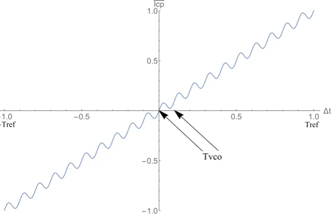
The characteristic of an SSPD is shown in figure 2.5. Due to the sinusoidal output of the VCO, the phase-current transfer of the sub-sampling loop is sinusoidal with a periodicity of 2π in the phase domain orTvco in the time domain.
The phase-current transfer of a PFD without a DZ shown in figure 2.2, has sawtooth shape with a periodicity of 2π in the phase domain orTref in the time domain.
By combining these two characteristics and characteristic is shown in figure 3.4. After taking the derivative around the lock point a loop gain is obtained. The loop gain from other definitions may lead to more conservative estimates, possibly allowing for a design with better dynamic behaviour. However, by using this definition and resulting optimistic value for the loop gain, loop stability is ensured.
Tref -Tref
Tvco
-1.0 -0.5 0.5 1.0 Δt
-1.0
[image:25.595.105.437.192.404.2]-0.5 0.5 1.0Icp
Figure 3.4.: The combined time-current transfer of the sub-sampling and frequency loops without a DZ.
A point that wasn’t touched upon in the paper by Gao [9], is the influence of the gain reduction implementation on loop stability.
As explained in section 2.3, the feedback gain should just be high enough to make the charge pump noise negligible. If the feedback gain becomes higher than that point, the loop filter capacitance must become very large for loop stability without gaining any noise benefit. The feedback gain can then be said to be unnecessarily high and should be reduced.
In [9] this was done by adding a pulser block that only turns on the charge pump for a fraction τpul of the sampling period Tref. This reduces the feedback by a factor
τpul
Tref.
sample frequencyTs=Tref and the hold-pulse width-scaling factorρ.
Hzosh(ω) =
1−exp−jωρTs
2
jωρTs
2
= sin (
ωρTs
2 )
ωρTs
2
·exp−jωρTs
2 (3.9)
For ρ = 1 the pulse width is equal to Ts. One can quickly deduce that the transfer
function magnitude then contains zeroes at multiples of the sample frequency. This is illustrated by the Mathematica plots 3.5a and 3.5b in which the magnitude and phase are plotted from left to right forρ= 1,0.1,0.01. The sample frequency for this example is 1×10⁶rad/s.
For the green plot ρ = 1 and the first zero occurs at 1×10⁶rad/s and gives a dip of which the magnitude is limited by the calculation accuracy. The subsequent zeroes are at every multiple of the sample frequency.
The Orange plot shows what happens when ρ = 0.1. By making the hold-pulse ten times narrower, the sample frequency is effectively increased by the same amount. This can be seen by observing that the first and subsequent zeroes for the orange graph are at ten times higher angular velocity compared to the green graph.
By increasing ρ again by ten times the blue graph is obtained. As before the sample frequency is effectively also increased tenfold making the zeroes move to ten times higher angular velocities.
All of this is a problem because the VCO output frequency that needs to be sampled is exactly an integer multiple of the reference frequency. Without any loop gain in the lock point there is no loop noise suppression, meaning increased phase noise at the SSPLL output. Because of this effect the gain reduction implementation as used in [9] is likely the best choice for achieving a low PLL FOM.
105 106 107 108
-60
-40
-20
0
w(rad/s)
Magnitude Plot
(a) Magnitude plot of the ZOSH transfer func-tion forρ= 1,0.1,0.01.
105 106 107 108
-150
-100
-50
0
w(rad/s) Phase Plot
(b) Phase plot of the ZOSH transfer function forρ= 1,0.1,0.01.
3.2. Channel Switching simulations
In this section simulations will be used in order to find out more about the dynamic be-haviour of Sub-Sampling Phase-Locked Loops and more specifically the channel switch-ing behaviour. Channel switchswitch-ing is when a PLL is tuned from one output frequency to another by changing the division ratio in the feedback.
The goal of these simulations is to find out how the following SSPLL parameters influ-ence the channel switching behaviour, with an emphasis on the time it takes to regain phase lock:
> Size of the Dead-Zone (DZ): a distinct difference between a classic PLL using a Phase-Frequency Detector (PFD) and an SSPLL is the dual loop structure and the presence of a DZ in the frequency loop. The DZ ensures that in lock the phase noise is determined by the sub-sampling loop. In [8] it is shown that the DZ influences the SSPLL reaction to a perturbation, this section will examine if this is also the case for channel switching behaviour.
> Loop Gain Ratio (LGR): the presence of two loops in an SSPLL and therefore two loop gains, begs the question if there is an LGR that optimises channel switching behaviour. LGR is defined as the ratio between the sub-sampling and the frequency loop feedback gains: βSSP D
βP F D .
> Loop BandWidth (LBW): in most dynamic systems the LBW plays a role in the behaviour. Therefore the relation of the channel switching behaviour with respect to the LBW will be studied.
The simulation model that will be used was introduced in section 3.1. The block schematic and phase domain model of the SSPLL can be found in figures and 2.6 and 2.7.
3.2.1. Channel Switching Simulation Setup
In these channel switching simulations the quantity of interest is the time it takes for the output frequency to settle to within a certain error from the pre-set division ratio. However, becauseVtuneis directly related to the output frequency and an instantaneous
frequency is more difficult to determine than a voltage,Vtunewill be evaluated and give
the same information. Using the equation:
Vtune=
fout−ff r
KV CO
= N·fref −ff r KV CO
(3.10)
theVtune for a certain multiplication integer N is known. In this simulation fref = 50
MHz,ff r = 2.2 GHz,N = 45 and Kvco = 50 MHz/V corresponding to aVtuneof 1 V.
The settling time will be the measured quantity and is defined as the time when Vtune
falls within a chosen boundary of its final value. The maximum simulation time is 25µs which is more than enough for the PLL to lock, given that the range of interest is sub-10µs as was explained in chapter 1. If the PLL is not able to lock within that time a settling time of 25µs will be recorded. By recording 25µs instead of “no lock” the results can be included in numerical result graphs.
In classic control theory a 2% error limit from the theoretical steady-state value is often used. Due to the similarity of those applications and a PLL the same limit is maintained here.
To find the influence of the DZ on the dynamic behaviour two variations of the model are simulated. In the original model the DZ was Tref/2, because this was how it was
implemented in [9].
In the publication [8] it was proposed to remove the DZ, because of its negative effect on the robustness to perturbations of the SSPLL. Therefore, the second choice for the DZ is to reproduce the implementation of [8] and remove the DZ.
Proposed SSPLL Robustness Improvement
Although [8] showed that the robustness to perturbations was improved compared to [9], the output phase noise was higher. The idea behind the SSPLL is to use only the SSPD for the phase lock, because of its high detection gain giving lower output phase noise than a traditional PFD. A PFD is used to get the correct frequency lock, because the SSPD cannot distinguish between multiples of the frequency it samples. This means that on its own an SSPD doesn’t correct the loop output towards the desired integer multiple of the reference frequency. The DZ is added so that when the correct frequency is locked the noise performance is not degraded by the PFD. Therefore, by removing the DZ entirely a core advantage of the SSPLL is lost.
A compromise between having a DZ ofTref/2 and no DZ, is to reduce the size of the DZ
without removing it. This should give both the noise benefit of the original SSPLL and
have similar robustness to perturbations as was shown by removing the DZ. Looking again at figure 2.5 shows that the next zero crossing after the lock point is at a phase difference of Tvco/2. Therefore, choosing the size of the DZ smaller than Tvco/2 only
leaves the desired lock point. To change the size of the PFD DZ shown in figure 3.2 the ”CLK” signal of the second flip-flops should be changed. For a DZ of Tvco/2 the “CLK”
signal for the pair of flip-flops on the right-hand side should be changed to the inverted VCO output, instead of “!REF” and “!DIV”. This PFD with a DZ ofTvco/2 is shown in
figure 3.6. The changes compared to the PFD with a DZ of Tref/2 from figure 3.2 are
green. This solution both reduces the size of the DZ providing the mentioned benefits and can be implemented with no additional components using existing signals.
Q Q
SET
CLR Q
Q
SET
CLR
UP
Q Q
SET
CLR Q
Q
SET
CLR
[image:29.595.105.430.236.453.2]DOWN
Figure 3.6.: Schematic of a PFD with a DZ ofTvco/2.
Expectations for the Simulations
Going into the simulations there where no expectations of what effect the DZ or LGR would have on the channel switching behaviour, because there was no theoretical de-scription available or conceived beforehand. The LGR will be varied from 1 to 450 in course steps with the intent of revealing a pattern or relation to the settling time from the simulation results. The simulation will be run with the DZ removed and then with the DZ set to the size of Tref/2 andTvco/2.
For the effect of LBW a theoretical basis was found in [12] of which a summary is given here:
of a PFD-PLL falls within an arbitrary boundary α that indicates a chosen relative frequency error, after switching from one division ratio “N1” to another “N2”.:
|1− N1
N2| ·(1−g(t)u(t))≤α (3.11) Where g(t) is the time domain closed loop transfer function and u(t) the unit step function. For a type-II integer-N PLL withξ≤1, g(t) is given by:
g(t) = 1−[cos(p1−ξ2ω
nts)−
ξ
p
1−ξ2sin( p
1−ξ2ω
nts)] exp−ξωnts (3.12)
For the settling time, only the envelope of the signal is important resulting in the fol-lowing expression forα:
|1−N1
N2| ·
√
2 exp−ξωnts ≤α (3.13)
This expression can be rewritten to an expression for the settling timets:
ts=
√
2 ωn
log(
√
2(1−NN12)
α ) (3.14)
Equation 3.14 reveals an inverse relation forts with the natural frequencyωn and
there-fore with the LBW of the PLL defined as 2.5ωn. A derivation of this bandwidth can be
found in section 9.6 from [12].
Using equation 3.14 and substituting the valuesN1 = 44,N2 = 45,LBW = 2π2.50M Hz ,wn= LBW2.5 = 2π1e6rad/sand α= 0.02 the calculated settling time ists= 0.1µs.
The LBW is set to 0.63, 1.25, 2.50 and 5.00 MHz.
Tradional PFD Simulations Result for Comparison
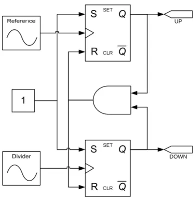
To have a ground for comparison for the upcoming simulations a PLL with a regular PFD is simulated. The schematic of the PFD is shown in figure 3.7. The LBW is set to 2.50 MHz and the simulations were run using the script found in appendix A. This means that the expected tune voltage is 1 V.
The simulatedVtunevoltage is shown in figure 3.8. The simulation result shows that the
tune voltage settles to 1 V with an overshoot going to 1.5 V.
The simulated 2% settling time is 0.81µs. It turns out that equation 3.14 gives rather optimistic values and that in practice settling times are longer.
It should also be noted that equation 3.14 does not take into account any SSPLL specific parameters like LGR or DZ. Therefore, the predictive value for an SSPLL is likely to be worse.
These results and figure 3.8 can be used as a reference for the result of the upcoming simulations done with the SSPLL.
SET
CLR
UP
SET
CLR
DOWN
[image:31.595.170.365.131.329.2]Figure 3.7.: Schematic of a standard PFD.
Simulation Setup Variables Table
[image:32.595.120.538.161.387.2]The simulation parameters and values are shown in table 3.1.
Table 3.1.: Summary table of the channel switching simulation setup.
Parameter Value(s)
fref (Hz) 50e6 Aref (V) 0.5
ff r (Hz) 2.2e9
Avco(V) 0.5
Kvco(Hz/V) 50e6
N1 44
N2 45
fout(Hz) 2.25e9
Vtune(V) 1
Icp(A) 20e-6
Vod(V) 200e-3
ξ 1
Apert(V) 0.5
Type of the DZ linear binary
Size of the DZ none Tref/2 Tvco/2
LGR 1 25 50 75 100 125 150 200 250 300 350 400 450
LBW (Hz) 0.63e6 1.25e6 2.50e6
3.2.2. Channel Switching Simulation Results and Discussion
The simulations were run using the script found in appendix A. The recorded settling times are shown in figure 3.9, 3.14 and 3.12.
The y-axis in the graphs indicates the settling time in µs. The x-axis covers the range of LGRs that were simulated. The various LBWs are indicated by different colors and shapes shown in the legend on the right of the graphs.
For reference, an example of the simulatedVtunefor a correctly locking PLL is shown in
figure 3.8.
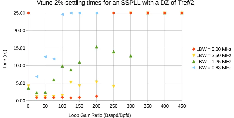
Phase-Frequency Detector With a Dead Zone of Tref/2
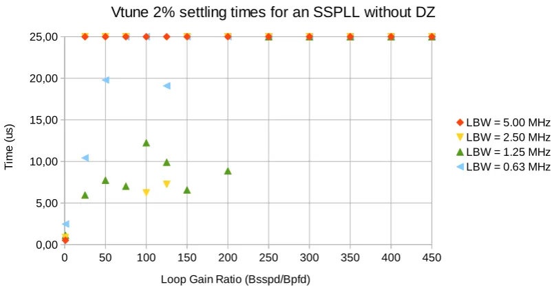
Looking at the simulation results shown in figure 3.9, the fastest settling times for an SSPLL with a DZ of Tref/2 are at an LGR of 25.
For comparison to the traditional PFD, the simulatedVtunefor an LGR of 25 and LBW
[image:33.595.67.474.346.551.2]of 2.50 MHz is shown in figure 3.10. Compared to figure 3.8 the response is a lot slower.
Figure 3.9.: The 2% Vtune settling times of an SSPLL with a DZ of Tref/2 versus loop
gain ratios.
For an LGR of 1 and LBW of 0.63 and 5.00 MHz the PLL does not achieve lock within 25µs. The graphs of Vtune for LBW is 0.63 MHz is shown in figure 3.11. It can be seen
that the loop overshoots the 1 V target. Looking closely at Vtune, after overshooting the
lock. The frequency loop takes a very long time react. When it finally does react, it overshoots the 1 V target again and the story repeats. The same goes for LBW is 5.00 MHz.
Looking again at figure 3.9 there is a trend for longer settling times as the LGR gets higher. The results also reveal that for an SSPLL with a DZ ofTref/2 the LGR should
at least be lower than 300, because the SSPLL then fails to lock at any LBW. In the region between LGR 1 and 100 the SSPLL locks with every LBW, though some results are almost 25µs.
Figure 3.10.: Graph ofVtunefor an SSPLL with a DZ ofTref/2, LGR of 25 and LBW of
2.50 MHz.
Figure 3.11.: Graph ofVtune for an SSPLL with a DZ of Tref/2, LGR of 1 and LBW of
0.63 MHz.
Phase-Frequency Detector Without a Dead Zone
The channel switching simulation results for the PFD without DZ are shown in figure 3.12. For the SSPLL without a DZ the lowest settling times are at an LGR of 1. Compared to 3.8 the simulated graph of Vtune shown in figure 3.13 is very similar. An
[image:35.595.69.472.257.466.2]important difference is that there are some minor ripples on the final voltage. The severity of these ripples became less after decreasing the simulation step time. It is therefore believed that these ripples are due imprecision if the simulation. By removing the DZ the lock point of both loops has to be exactly the same. Otherwise there could be a back and forth between two very similar, but not identical lock points. With more computing power this imperfection could be studied further.
Figure 3.12.: The 2% Vtune settling times of an SSPLL without a DZ versus loop gain
ratios.
Above LGR 1 the results are inconsistent, but unlike for the DZ of Tvco/2 it is hard to
say whether those points represents situations where the SSPLL does not lock correctly. This is because the final Vtune already contains a lot of remaining activity due to the
lack of DZ.
Phase-Frequency Detector With a Dead Zone ofTvco/2
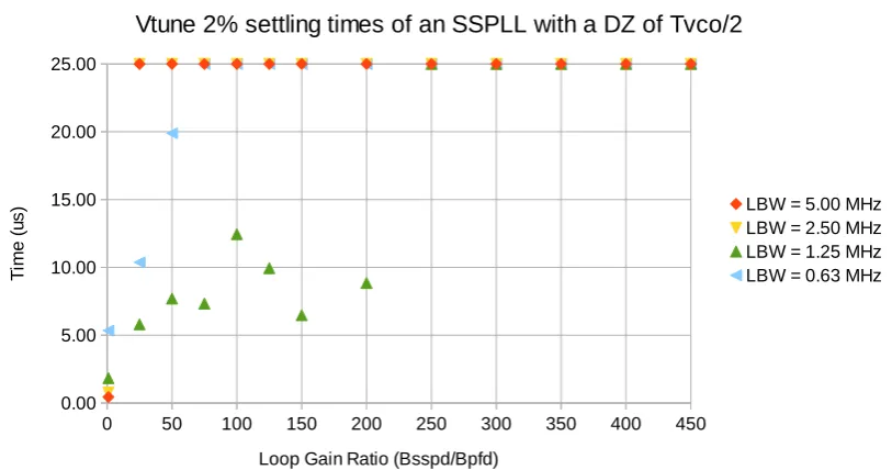
In figure 3.14 the results are shown for the SSPLL with a DZ of TV CO/2. The lowest
settling times are at an LGR of 1. The graph of Vtune for a LGR of 1 and LBW of
2.50 MHz is shown in figure 3.15.
[image:36.595.127.534.407.621.2]Compared to figure 3.8 the response is slower, but again due to the DZ the final voltage has no remaining PFD activity. Compared to figure 3.10 the response is faster.
Figure 3.13.: Graph ofVtunefor an SSPLL without DZ, LGR of 1 and LBW of 2.50 MHz.
Figure 3.14.: The 2%Vtune settling times of an SSPLL with a DZ of Tvco/2 versus loop
gain ratios.
Only for LBW equal to 1.25 MHz and 0.63 MHz there are results that lock within 25µs for an LGR higher than 1. Zooming in on the final voltage for LGR is 50 and a LBW of 2.50 MHz shown in figure 3.16, it can be seen that the final voltage shows activity despite the presence of a DZ. This means that the SSPLL is not actually locked correctly. This also goes for all other points with LGR higher than 1.
For an SSPLL with a DZ ofTvco/2 only LGR 1 works for all frequencies and also shows
the fastest settling times. There are so few correctly locked simulation results available that it is impossible to draw any meaningful conclusion about a trend.
Figure 3.15.: Graph ofVtune for an SSPLL with a DZ ofTvco/2, LGR of 1 and LBW of
2.50 MHz.
Figure 3.16.: Zoomed graph of Vtune for an SSPLL with a DZ ofTvco/2, LGR of 50 and
3.2.3. Preliminary Conclusion About the Channel Switching Simulations
So far it has become clear that the LBW has an inverse relation with the settling time and that a higher LGR either breaks the SSPLL or makes the settling time longer. Only in the case of an SSPLL with a DZ ofTref/2, an LGR higher than 1 lowered the settling
time.
In figure 3.17 the fastest simulations settling times for the different DZs are shown. The graph seems to suggest that the relation between the DZ and settling time is that a bigger DZ has slower settling behaviour. The graph also shows the theoretical settling time that was discussed in subsection 3.2.1. As stated previously, the theory underestimates the settle time. The match to the simulation results without a DZ could be improved by multiplying equation 3.14 by 6.
Figure 3.17.: Graph comparing the settling times for the different DZs.
The simulations showed that the 2% limit taken from classical control theory to measure the settling time turns out to be too big, because it doesn’t exclude some wrong lock points. The settling limit needs to be adjusted for further simulations.
Upon further reading of [8], the paper also noted a maximum current relation between the two loops in an SSPLL. This next section will expand upon this to derive a maximum for the LGR.
Another insight was that the PFD with DZ as used by [9] and shown in figure 3.2 is not linear, but binary due to the second pair of flip-flops not being reset. The consequences of this will also be discussed in the next section. In section 3.4 a linear PFD with DZ will be proposed to see if it shows any benefits with regard to dynamic behaviour compared to the binary PFD with DZ used previously.
3.3. Loop Gain Ratio Analysis
From the results of the settling simulations a rough insight evolved into what the relations between LGR, LBW and DZ are. However a theoretical explanation is still lacking. The block schematic of an SSPLL can be found in figure 2.6 and its phase domain model in figure 2.7.
In [8] a relation between the average current of the sub-sampling and frequency loop is given to ensure proper control action of the combined loop. In the paper it is argued that the time-current transfer function of the sub-sampling and frequency loop has to be superimposed to get the combined transfer. While it is more common to look at the phase-current transfer of a PLL, in this case the time-current transfer gives the better picture. The SSPLL is unique in that it has two loops that operate with different frequencies. The frequency loop operates using the reference and divided VCO output. However, the sub-sampling loop operates using the reference and direct VCO output. This difference means that 2π has a different meaning in the two loops. The frequency loop defines 2π as a period of the reference Tref. The sub-sampling loop defines 2π
as a period of the VCO Tvco. Using the conventional phase-current transfer would be
confusing because it would be unclear what the meaning of 2π phase difference would indicate. By going to the time domain this ambiguity is solved.
The time-current transfer of the individual linear PFD without DZ from figure 2.2 and SSPD from figure 2.5, are shown in figure 3.18 and 3.19. The combined time-current transfer is shown in figure 3.20. For the purpose of illustration the feedback division factor N is equal to 10 in this section.
The paper goes on to say that in order to ensure that only one lock point exists, this combined transfer should have positive average current output for positive time differ-ences and negative average current output for negative time differdiffer-ences. In this way the combined characteristic is able to control the loop to the right integer frequency. As explained in chapter 2 the SSPD alone does not have this property, precisely because its characteristic does not have this sign continuity for positive or negative phase/time differences. Together with expressions for the average output currents of the SSPD and PFD Isspd and Ipf d from [9], this results in the following equations that need to be
satisfied to maintain the proper control action in an SSPLL:
Isspd+Ipf d ≥0 (3.15)
−Isspd≤Ipf d (3.16)
Isspd=Avco·
2Icp
Icp
sin(∆φvco)
τpul
Tref
(3.17)
Ipf d =
Icp
2π∆φdiv (3.18)
Where Isspd and Ipf d are the average output currents of the SSPD and PFD, Avco the
transconduc-tance overdrive voltage andτpul the gain reduction pulse duration.
Tref
-Tref
-1.0 -0.5 0.5 1.0 Δt
-1.0
[image:40.595.161.494.109.327.2]-0.5 0.5 1.0Icp
Figure 3.18.: The time-current transfer of the frequency loop without a DZ.
Tref -Tref
Tvco
-1.0 -0.5 0.5 1.0 Δt
-1.0
-0.5 0.5 1.0Icp
Figure 3.19.: The time-current transfer of the sub-sampling loop.
Using this information a theoretical limit for the LGR can be derived. Because in [8] there is no DZ this case will be treated first and then be expanded upon to the cases
[image:40.595.163.494.373.589.2]with a DZ. For all analysis in this section it is assumed that:
Tref =N·Tvco (3.19)
∆φdiv = ∆t·ωref = ∆t·
2π Tref
= ∆t· 2π
N ·Tvco
(3.20)
∆φvco = ∆t·ωvco = ∆t·
2π Tvco
= ∆t·2π·N
Tref
(3.21)
Where ∆φdivis the phase difference and ∆tthe time difference between the zero-crossing
of the reference frequency and divided VCO frequency,ωref the angular frequency of the
reference, Tref the reference period, φvco is the phase difference between the reference
frequency and VCO frequency,ωvco the angular frequency of the VCO andTvcothe VCO
period.
3.3.1. Loop Gain Ratio Boundary for a linear PFD without a Dead Zone
For correct operation of the SSPLL the sign of the time-current characteristic of the combined loop, must be positive for a positive time difference and negative for a negative time difference. Looking at figure 3.20 it can be seen that for an SSPLL without a DZ the boundary of this condition is found when the time difference ∆t= 34Tvco. At that
time difference the sinusoidal transfer of the SSPD is at its first minimum starting from
Tref -Tref
Tvco
-1.0 -0.5 0.5 1.0 Δt
-1.0
[image:41.595.103.436.406.618.2]-0.5 0.5 1.0Icp
the lock point. Using this data and equation 3.16 the following relations are derived:
∆t= 3 4Tvco =
3
4NTref (3.22) ∆φdiv =
3
4N2π (3.23)
∆φvco =
3
42π (3.24)
−Isspd≤Ipf d (3.25)
−Avco·
2Icp
Icp
sin(∆φvco)
τpul
Tref
≤ Icp
2π∆φdiv (3.26)
−Avco·
2Icp
Vod
·sin(3 4 ·2π)·
τpul
Tref
≤ Icp
2π 3
4N2π (3.27)
τpul
Tref
≤ 3Vod
8N Avco
(3.28)
Equation 3.28 represents the maximum gain reduction factor for correct operation of the dual loop structure. With this equation the maximum LGR can be derived, whereβsspd
andβpf d represent the sub-sampling and frequency loop open loop gains from [9]:
βpf d =
Icp
2πN (3.29)
βsspd=Avco·
2Icp
Vod
· τpul
Tref
(3.30)
LGR= βsspd βpf d
=
Avco·2VIodcp ·Tτpulref Icp
2πN
(3.31)
LGRmax=
Avco·2VIodcp ·8N A3Vodvco Icp
2πN
= 3π
2 ≈4.7 (3.32)
3.3.2. A Linear Phase-Frequency Detector with Dead Zone of Tref/2
Before moving on to analyse the LGR for a linear PFD with a DZ, its design is proposed as shown in figure 3.21. To make the binary PFD from figure 3.2 linear, a reset should be added to the second flip-flops. This reset should simply be the same as is used for the first pair of flip-flops. Like before, to make the DZ Tvco/2 the ”CLK” signal of the
second flip-flops should be the inverted VCO output. This is shown in figure 3.22 the changes are coloured green.
Q Q
SET
CLR Q
Q
SET
CLR
UP
Q Q
SET
CLR Q
Q
SET
CLR
DOWN
Figure 3.21.: Schematic of the linear PFD with DZ ofTref/2.
Q Q
SET
CLR Q
Q
SET
CLR
UP
Q Q
SET
CLR Q
Q
SET
CLR
DOWN
3.3.3. Loop Gain Ratio Boundary for a linear PFD with a Dead Zone
Now the same derivation can be done using the linear PFD with DZ ofTref/2 shown in
figure 3.21. The introduction of a DZ ofTref/2 changes the PFD time-current transfer
as shown in figure 3.23.
The PFD now only produces an output current when the time difference is greater than Tref/2. This also means that the PFD effectively loses half of its maximum average
output current Icp
2 . Combining this new PFD transfer with the SSPD transfer from
figure 3.19, the combined time-current transfer with a linear PFD DZ ofTref/2 is shown
in figure 3.24. This means that the time difference when the control condition from
Dead Zone of Tref/2
Tref -Tref
-1.0 -0.5 0.5 1.0 Δt
-1.0
[image:44.595.164.492.240.452.2]-0.5 0.5 1.0Icp
Figure 3.23.: The time-current transfer of the frequency loop with a linear PFD with DZ ofTref/2.
equation 3.16 should be evaluated is now ∆t= 34Tvco+ Tref2 when the division ratio N
is even, because this time-difference is where the SSPD transfer has its first minimum outside of the DZ. The assumption is still that Tref =N ·Tvco leading to the following
equations:
∆t= 3 4Tvco+
Tref
2 =Tvco( 3 4 +
N
2) =Tref( 3 4N +
1
2) (3.33)
∆φdiv= (
3 4N +
1
2)2π (3.34)
∆φvco= (
3 4+
N
2)2π (3.35)
−Isspd≤Ipf d (3.36)
−Avco·
2Icp
Vod
sin(∆φvco)
τpul
Tref
≤ Icp
2π∆φdiv− Icp
2 (3.37)
−Avco·
2Icp
Vod
·sin((3 4+
N
2)·2π)· τpul
Tref
≤ Icp
2π( 3 4N +
1 2)2π−
Icp
2 (3.38)
−Avco·
2Icp
Vod
·sin(3 4·2π)·
τpul
Tref
≤ 3Icp
4N (3.39)
τpul
Tref
≤ 3Vod
8N Avco
(3.40)
Where sin(N22π) = 0 is used.
The value for the maximum gain reduction factor is the same results as in equation 3.28. Therefore the maximum LGR is also the same 32π ≈4.7 as equation 3.32.
For N is odd the time difference should be changed to ∆t= 14Tvco+Tref2 , because of the
sinusoidal nature of the SSPD. The Ipf d now becomes three times lower resulting in a
three times lower maximum gain reduction factor τpul
Tref and LGR
π
2 ≈1.6.
Tref
-Tref
Dead Zone of Tref/2
-1.0 -0.5 0.5 1.0 Δt
-1.0
[image:45.595.102.436.427.643.2]-0.5 0.5 1.0Icp
Dead Zone of Tvco/2
If the DZ is reduced toTvco/2 as in figure 3.22, the PFD only produces an output current
when the time difference is greater thanTvco/2. This means that the starting point for
the analysis is nowTvco/2 instead of Tref/2. The SSPD characteristic now has its first
minimum outside of the DZ at ∆t= 14Tvco+ 12Tvco. The loss of average output current
in the PFD due to the DZ ofTvco/2 =Tref/(2N) is nowIpf d = I2cpπ∆φdiv = I2cpπ Nπ = I2cpN.
This gives the following derivation of the maximum gain reduction factor:
∆t= 1 4Tvco+
1 2Tvco =
3 4Tvco=
3
4NTref (3.41) ∆φdiv =
3
4N2π (3.42)
∆φvco =
3
42π (3.43)
−Isspd≤Ipf d (3.44)
−Avco·
2Icp
Vod
sin(∆φvco)
τpul
Tref
≤ Icp
2π∆φdiv− Icp
2N (3.45)
−Avco·
2Icp
Vod
·sin(3 42π)·
τpul
Tref
≤ Icp
2π 3 4N2π−
Icp
2N (3.46)
−Avco·
2Icp
Vod
·sin(3 42π)·
τpul
Tref
≤ Icp
4N (3.47)
τpul
Tref
≤ Vod
8N Avco
(3.48)
This gain reduction factor is three times less than equation 3.28. The maximum LGR for a SSPLL with a linear PFD with a DZ of Tvco/2 is therefore π2 for N is both even
and odd.
Dead Zone of Tvco/2
Tref -Tref
-1.0 -0.5 0.5 1.0 Δt
-1.0
[image:47.595.101.435.100.319.2]-0.5 0.5 1.0Icp
Figure 3.25.: The time-current transfer of the frequency loop with a linear PFD with DZ ofTvco/2.
Tref
-Tref
Dead Zone of Tvco/2
-1.0 -0.5 0.5 1.0 Δt
-1.0
-0.5 0.5 1.0Icp
[image:47.595.103.436.401.619.2]3.3.4. Loop Gain Ratio Boundary for a binary PFD with a Dead Zone
The PFD with DZ ofTref/2 as described in [9] is not linear but binary as shown in figure
3.2, because the second flip-flops are never reset. This causes the current output to not increase linearly to its maximum ofIcp when the time difference is greater thanTref/2.
Instead the output current is maximum for all time differences greater thanTref/2. The
time-current transfer for this binary PFD is shown in figure 3.28.
Dead Zone of Tref/2
Tref
-Tref-1.0 -0.5 0.5 1.0
Δt
-1.0
[image:48.595.164.493.196.406.2]-0.5 0.5 1.0 Icp
Figure 3.27.: The time-current transfer of the frequency loop with a PFD with binary DZ ofTref/2.
To find the maximum gain reduction factor the right-hand side of equation 3.16 now changes toIcp, instead of I2cpπ∆φdiv−Icp2 in case of the linear PFD with a DZ of Tref/2
(eq. 3.37).
This also means that there is no more difference between even and odd N. That is, because no matter at what time difference the SSPD characteristic has its minimum outside of the DZ, the average current output of the PFD is maximum. Therefore, the time difference at which to evaluate the average output current from the SSPD remains the same at ∆t= 34Tvco+
Tref
2 .
∆t= 3 4Tvco+
Tref
2 =Tvco( 3 4 +
N
2) =Tref( 3 4N +
1
2) (3.49)
∆φdiv= (
3 4+
N
2)2π (3.50)
∆φvco= (
3 4N +
1
2)2π (3.51)
−Isspd≤Ipf d (3.52)
−Avco·
2Icp
Vod
sin(∆φvco)
τpul
Tref
≤Icp (3.53)
−Avco·
2Icp
Vod
·sin((3 4+
N
2)·2π)· τpul
Tref
≤Icp (3.54)
τpul
Tref
≤ Vod
2Avco
(3.55)
Because this result for τpul
Tref is different from equation 3.28 the maximum LGR is also
different:
LGR= βsspd βpf d
=
Avco·2VIodcp · τpul
Tref
Icp
2πN
(3.56)
LGRmax=
Avco·2VIcp
od ·
Vod
2Avco
Icp
2πN
= 2πN (3.57)
Dead Zone of Tref/2
Tref -Tref
-1.0 -0.5 0.5 1.0 Δt
-1.0
-0.5 0.5 1.0 Icp
Dead Zone of Tvco/2
The size of the DZ is decreased to Tvco/2 by clocking the right-hand side pair of
flip-flops with the inverted VCO output in figure 3.2 as shown in figure 3.6. The changes are shown in green. The time-current transfer of the binary PFD with a DZ ofTvco/2 is
shown in figure 3.29.
Because the second pair of flip-flops is not reset, the average output current of the PFD can now only change everyTvco seconds of time difference. Therefore if the time
difference is only just longer than the DZ Tvco/2, the average output current will be
Ipf d = Icp · TTvco
ref. In other words, the time-current transfer is now a stair case with
minimal step size Icp
N assuming Tvco
Tref =
1
N. The combined time-current transfer is shown
in figure 3.30.
Dead Zone of Tvco/2
Tref -Tref
-1.0 -0.5 0.5 1.0 Δt
-1.0
[image:50.595.165.491.271.479.2]-0.5 0.5 1.0 Icp
Figure 3.29.: The time-current transfer of the frequency loop with a binary PFD with DZ ofTvco/2.