warwick.ac.uk/lib-publications
Original citation:
Donchev, Evgeniy, Pang, Jing S., Gammon, P. M., Centeno, Anthony, Xie, Fang, Petrov, Peter
K., Breeze, Jonathan D., Ryan, Mary P., Riley, D. Jason and Alford, Neil McN.. (2014) The
rectenna device : from theory to practice (a review). MRS Energy & Sustainability - A Review
Journal, 1 .
Permanent WRAP URL:
http://wrap.warwick.ac.uk/62338
Copyright and reuse:
The Warwick Research Archive Portal (WRAP) makes this work by researchers of the
University of Warwick available open access under the following conditions. Copyright ©
and all moral rights to the version of the paper presented here belong to the individual
author(s) and/or other copyright owners. To the extent reasonable and practicable the
material made available in WRAP has been checked for eligibility before being made
available.
Copies of full items can be used for personal research or study, educational, or not-for profit
purposes without prior permission or charge. Provided that the authors, title and full
bibliographic details are credited, a hyperlink and/or URL is given for the original metadata
page and the content is not changed in any way.
Publisher’s statement:
This article has been published in a revised form in
http://dx.doi.org/10.1557/mre.2014.6
.
This version is free to view and download for private research and study only. Not for
re-distribution, re-sale or use in derivative works.
© © Materials Research Society 2014
A note on versions:
The version presented here may differ from the published version or, version of record, if
you wish to cite this item you are advised to consult the publisher’s version. Please see the
‘permanent WRAP url’ above for details on accessing the published version and note that
access may require a subscription
E. Donchev,1,∗ J. S. Pang,1 P. M. Gammon,2 A. Centeno,3 F. Xie,1 P. K. Petrov,1 J. Breeze,1 M. P. Ryan,1 D. J. Riley,1 and N. McN. Alford1 1Department of Materials, Imperial College London, London, SW7 2AZ, United Kingdom
2
School of Engineering, University of Warwick, Coventry, CV4 7AL, United Kingdom
3
iKhoza Nano-Characterization, Structural Control and Processing,
Malaysia-Japan International Institute of Technology, 54100 Kuala Lumpur, Malaysia
(Dated: April 20, 2014)
The Rectenna (RECTifying antENNA), which was first demonstrated by William C. Brown in 1964 as a receiver for microwave power transmission, is now increasingly researched as a means of harvesting solar radiation. Tapping into the growing photovoltaic market, the attraction of the rectenna concept is the potential for devices that, in theory, are not limited in efficiency by the Shockley-Queisser limit. In this review, the history and operation of this 40-year old device concept is explored in the context of power transmission and the ever increasing interest in its potential applications at THz frequencies, through the infra-red and visible spectra. Recent modelling ap-proaches that have predicted controversially high efficiency values at these frequencies are critically examined. It is proposed that to unlock any of the promised potential in the solar rectenna concept, there is a need for each constituent part to be improved beyond the current best performance, with the existing nanometer scale antennas, the rectification and the impedance matching solutions all falling short of the necessary efficiencies at THz frequencies. Advances in the fabrication, character-isation and understanding of the antenna and the rectifier are reviewed, and common solar rectenna design approaches are summarised. Finally, the socio-economic impact of success in this field is discussed and future work is proposed.
I. INTRODUCTION
The ever increasing global demand for clean renew-able energy is a crucial topic that has major economic and societal impact for our future on this planet. The sun is a constant source of energy, thus better harvest-ing its radiation would solve the energy challenge and help protect the environment. Conventional solar har-vesting is via the increasingly popular photovoltaic (PV) p-n junction solar cells. Although this field has seen great improvement over the last few decades since the first sil-icon solar cell was developed in 1941 at Bell Laborato-ries, its fundamental limitations discussed by Shockley and Queisser1 in 1961 puts an upper boundary on the efficiency at around 30% for single junction solar cells1 and 55% for multi-junction solar cells2. Due to the effi-ciency limits of solar cells, other solar-energy converting technologies are becoming increasingly attractive. An al-ternative solar energy converter concept is the Rectenna (RECTifying antENNA) device, which has achieved very high efficiencies at microwave frequencies, while at THz frequencies, it has been speculated that efficiencies ex-ceeding the Shockley-Queisser limit are achievable.
Fundamentally the Rectenna and the Solar Cell are similar as there is absorption of photons to generate a DC current. However, there is a substantial difference in their principles of operation. Solar cells are quantum devices, except for their anti-reflection coatings, and are only able to be understood and designed by the
applica-∗Corresponding author:
tion of quantum physics3, where light is perceived in its particle form, as photons. Hence, the efficiency is limited by the band gap energy of the active layers, where energy is lost due to low energy photons passing right through the material, and through heat loss from the high fre-quency photons. The rectenna device concept is differ-ent as it is based upon the wave nature of light, which is regarded as a propagating, oscillating electric and mag-netic field4. Similar to a low pass filter in electronics, the efficient absorption of solar radiation is limited by the cut-off frequency of the device, i.e. any wavelength below this frequency can be harvested.
FIG. 1. Block diagram of microwave rectenna and load. (Reprinted from [3], c2002 with permission from Elsevier)
alternating current (AC) in the conducting antenna. A low pass filter is used to form an impedance match be-tween the antenna and the rectifier, and passes the signal at the tuned operating frequency whilst blocking reradi-ation of higher order harmonic energy produced by the rectifier3,6–8. The rectifier (a diode) converts the input AC signal to a usable direct current (DC) which is trans-ferred to the load. A DC pass filter, consisting of an inductor in series, is used to smooth the rectified signal to DC whilst providing efficient transfer to the load.
[image:3.612.56.294.394.523.2]The antenna dimensions are of the same length scale as the targeted frequency5. Therefore, for microwave fre-quencies, the antenna is relatively large (cm to mm scale) compared to that required for infrared (µm scale) and optical frequencies (nm scale). Due to its smaller size, it will be difficult to incorporate the aforementioned fil-ters into the design of a rectenna for solar energy collec-tion. Therefore the components of the solar rectenna are reduced to just the Antenna and Rectifier (Figure 2)9. The removal of the low-pass filter from this design en-ables broadband frequency harvesting up to the cut-off frequency of the device, although it introduces the diffi-culty of impedance matching the antenna and rectifier, resulting in a potential drop in efficiency. Losses in trans-ferring the rectified DC signal to the load are dependent on the diode behaviour. However, appropriate design of a DC pass filter would make its use possible in this configuration99,100.
FIG. 2. Block diagram of solar rectenna and load. (Reprinted from [9], cIOP Publishing. Reproduced by permission of IOP Publishing. All rights reserved.)
There are two families of designs for rectenna solar energy collectors. Bailey10 proposed that each antenna element is attached to its individual rectifier and the DC outputs are combined (see Figure 5). The immediate concern here is that the small voltage predicted from the antenna elements may be insufficient for rectifica-tion to occur in the attached diode element3. The only way to overcome this is to design a diode which turns on at a voltage as low as that arising from the single antenna element. The other design is by Kraus11, who suggested that the electrical oscillations from many
an-tenna elements be combined in a particular phase rela-tionship, then delivered together to the rectifier. Limita-tions in this design arise from the need for spatial coher-ence across all the antenna elements feeding the signal to the diode3. This can be minimised by appropriate design and high quality fabrication of the antenna elements.
The aim of this article is to review key research in the development of the rectenna device as an alternative or in addition to conventional solar cell technology. We aim to expand upon a few short reviews, [3–5,9,100,105], that have been published, bringing the reader up to date with a more detailed overview of the device. This article will be the first to bring together all relevant research not only on the rectenna as a whole device, but also the re-search on its two main components – the antenna and the rectifier. The next section will briefly describe the history of the device and how the initial application of microwave power transmission (MPT) was later modi-fied to a solar energy harvesting alternative. SectionIII
will analyse and discuss the many publications on ex-perimentally and theoretically derived device efficiencies. Breakthroughs in modelling and fabricating the antenna and rectifier will be reviewed in SectionIVandV respec-tively. SectionVIwill bring together all components and look at different rectenna architectures, which show po-tential for efficient operation at solar frequencies. We will discuss the socio-economic impact of the research in this field and proposed future work in SectionVIIbefore com-pleting the article with a short summary in SectionVIII.
II. HISTORY OF THE RECTENNA DEVICE
The rectenna concept was initially proposed for wire-less power transmission by William C. Brown of the Raytheon Company in the 1960’s. At the time, Brown, a pioneer of microwave power transmission, was faced with a challenge of how to efficiently receive and convert to DC power an incoming microwave beam. Wireless power transmission was not a new concept as it had begun with the ideas and demonstrations by Tesla in 1899 using ra-dio waves12. Tesla managed to demonstrate this concept although never found an applicable route into its com-mercialisation.
FIG. 3. Left: W.C. Brown holding the rectenna helicopter platform. Right: In flight demonstration of the rectenna helicopter on October 1964. (Reprinted from [17])
horn-illuminated ellipsoidal reflector that focused the mi-crowave beam into a trapezoidal horn at a 20 ft distance where the microwaves were converted to DC power by the rectifier13. Using this first design, Brown constructed and flew thirty feet above his lawn a small tethered helicopter that he had built with his son in his own workshop13. Although this concept worked, Brown was aware of the flaws in his system and continued to work on other pos-sibilities.
In 1963, Brown met with his colleague and friend Roscoe George, a professor at Purdue University who had been working on a microwave point-contact semicon-ductor diode15. Following discussions regarding his chal-lenge, a device which is now known as “Rectenna” was conceived. The proposed solution was patented in 1969 and consisted of taking individual full-wave rectifiers out of the waveguide, attaching them to half-wave dipoles, and placing a reflecting plate behind the structure16. The first microwave rectenna was built by R.H. George at Purdue University but conceived at Raytheon Company in 1963, shown in Figure4. Later in 1964, Brown built a helicopter which had an array of 28 such Rectennas. The helicopter was demonstrated in flight 60 ft above a trans-mitting microwave beam on the CBS Walter Cronkite News in October 1964. Figure 3 shows some impressive images of this historic event. The interested reader is re-ferred to Brown’s recollection on “The History of Power Transmission by Radio Waves” in [13], where all the inter-esting details and facts about the invention of this device can be found.
Following this invention, microwave power transmis-sion became very popular and many potential applica-tions were researched. An interesting one is the solar
FIG. 4. The first rectenna. Conceived at Raytheon Company in 1963, built and tested by R.H. George at Purdue University. It was composed of 28 half–wave dipoles, each terminated in a bridge rectifier made from four 1N82G point–contact, semiconductor diodes for operation at 2.45 GHz. A power output of 7W was produced at 40% efficiency. (Reprinted from [13], c1984 IEEE. Reprinted, with permission, from IEEE)
[image:4.612.318.562.339.510.2]a collaborative three year project together with Brown in 1977 called the “DOE/NASA Satellite Power System Concept Development and Evaluation Program”. The work ended in 1980 with much success in developing new ideas in the design of transmission technology and rectenna arrays however did not attract further funding. Although this was the end of the SPS initiative in the US, some experimental studies of the concept were seen in the 1990s in Yamasaki, Japan24,25. The interested reader is referred to Glaser’s overview of SPS progress in [26].
The developments from the SPS project yielded other applications involving microwave transmission and rectenna, such as intersatellite power transmission27, in-cluding utility power satellites28, mechanical actuators for space-based telescopes29, small dc motor driving30, short range power transfer as for example between two parts of a satellite, RF identification tags (RFID) and biomedical implants31. These applications all include single band rectenna operation. Hagerty et al31 have shown a broadband rectenna array for microwave opera-tion to be used in low-power indoor sensor networks and RF energy recycling. Recent publications have shown a compact printed rectenna that can be used to supply DC power to electrical devices supporting data communica-tion systems32.
The idea of exploiting the wave nature of light, or so-lar radiation, and converting its energy into usable direct current by the use of antennas, originated as part of a NASA summer project in the late 1960s undertaken by J.C. Fletcher of NASA and R.L. Bailey of the University of Florida4. The first official report of this concept was published by Bailey in 197210. In this paper, he named his device the “Electromagnetic Wave Energy Converter (EWEC)” and suggested an artificial pyramid or cone structure as antennas, analogous to those found in na-ture and similar to dielectric rod antennas. The paper described pairs of pyramids as modified dipole antennas, each pair electrically connected to a half-wave rectifying diode, filter and load. This invention is fundamentally very similar to the initial microwave rectenna proposed by Brown, but it is modified so that the antenna and rectifier operate at much high frequencies to harvest so-lar energy. The device called by Bailey EWEC is now referred to as a Solar Rectenna.
Bailey’s first publication on the subject in 1972 served as a proof of concept as he showed the broadband char-acteristics of his pyramidal antennas by tests at 100-1000 MHz. Following this, in 1973, Fletcher and Bai-ley published a patent33 on the EWEC concept. Later in 1975, in their final report, Bailey et al34 presented their theoretical work highlighting the importance of fu-ture research into optimised antenna design and fabrica-tion, while not forgetting that rectification of the signals was an equally critical issue and a significant challenge4. These two components of the rectenna solar energy har-vester are now of equal research interest (see SectionsIV
&V).
[image:5.612.320.560.50.358.2]Later, alternative rectenna structures were proposed
FIG. 5. The EWEC concept by Fletcher & Bailey. Each broadband conical antenna is connected to a rectifying diode, filters and load. (Reprinted from [33])
and patented by Marks35–38, who was inspired by the earlier half-wave rectifier EWEC concept. His first patent in 1984 was a device with arrays of submicron crossed dipoles on an insulating sheet with fast full-wave rectifiers35. Later in 1988, Marks was first to patent antenna-like cylinders attached to asymmetrical metal-insulator-metal (MIM) diodes for rectification37. MIM diodes are one of the most promising rectifiers for use in Infrared and Optical Rectennas and will be later dis-cussed (SectionV.B).
The first reported experimental evidence of a fabri-cated resonant nanostructure absorbing and rectifying at visible light frequency was published by Linet al39 in 1996. They recorded a short circuit current using a paral-lel dipole sub-nanostructures connected to a p-n junction for the rectification of the absorbed signal. Credit must be given also to Gustafson & Billman40 who first sug-gested harvesting visible radiation in 1974. Their work formed the basis of using optical diodes like the MIM diode.
FIG. 6. Brief timeline of the rectenna device - from concept for microwave power transmission to research focused on solar harvesting
In the following sections, we mainly focus on the key re-search in harvesting optical and infrared frequencies us-ing the rectenna concept.
III. EFFICIENCY LIMITS
The first rectenna device (Figure4), which was built in 1963, provided a 7 W power output with 40% efficiency13 designed to work at 2.45 GHz. This was the most com-monly targeted transmitting frequency for MPT because of its low attenuation through the atmosphere even in severe weather and being at the centre of the industrial, scientific, and medical (ISM) band meant that it was the most advanced and efficient transmitting technology.
This rectenna used half-wave dipole antennas to re-ceive the signal and point-contact semiconductor diodes for rectification. In later device attempts, the half-wave dipole antenna remained the preferred technology, but an increase in efficiency was mainly achieved by improving the rectifier performance, incorporating Schottky Bar-rier Diodes (SBD). From the early 1960’s until the early 1980’s there has been a steady increase in the experimen-tally demonstrated efficiency of the rectenna at 2.45 GHz (Figure 7a). Although Nahas7 first developed a model (using a distributed transmission-line technique includ-ing skin-effect losses) to simulate the top performance of a rectenna utilising a dipole antenna and a conventional SBD, his prediction of an 80% upper boundary (most of the losses came from the diode rectifier) was later
im-proved when Brown82experimentally demonstrated what is to date, the highest ever recorded efficiency at the 2.45 GHz band of 92%. This was made possible by us-ing the then well established Pt/GaAs Schottky diode and supported Brown’s predictions that 100% efficiency is possible for this device44,82.
In another attempt to model the efficiency, Gutman & Borrego51 predicted an upper boundary of 85% in-corporating numerous rectifier outputs interconnected to a common DC load. They used a closed-form analyt-ical circuit model and a computer-simulation model in an attempt to show that a higher output power can be achieved having an array of these components as opposed to a single rectenna element.
It is important to state that the conversion efficien-cies (η) considered here are simply defined as the ratio of the output power (Pout) over the power incident on the antenna (Pin),
η(%) = Pout Pin
×100 (1)
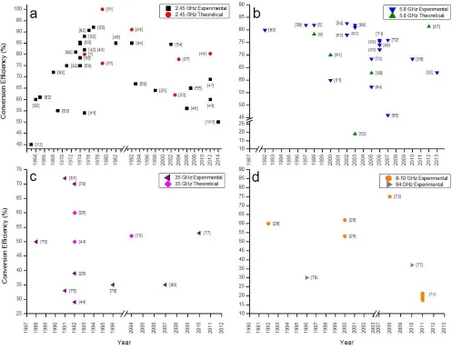
FIG. 7. Reported conversion efficiency (as defined by their authors) evolution over the years of a rectenna device for Microwave Power Transmission. Data points are split into Experimental and Theoretically derived values of efficiency. a) 2.45 GHz, b) 5.8 GHz, c) 35 GHz and d) 8-10 GHz and 94 GHz. [**] indicates the reference corresponding to the data point. Data collected from [3,5–7,10,11,13,25,28,29,32,41–51,53–82,101]
and shorted annular ring-slot47,53 antennas with all attempts returning efficiencies between 55 and 85% (see Figure 7a). The higher efficiencies reported all used GaAs Schottky diodes as opposed to conventional Si Schottky diodes, showing the importance of diode behaviour on device performance.
In the 1990’s a renewed interest in the solar power satellite (SPS) concept18–26 started a new focus of research into high efficiency rectennas and rectenna arrays operating at higher frequency than the mid-ISM band (2.45 GHz)41. With higher operating frequency, the device dimensions can be reduced conveniently from the point of SPS construction feasibility41. Also small size design can be appropriately implemented in a range of other applications such as a supply source in RFID31,55,58,64,68,77, wireless sensors31,47,58,77 and data communication systems32,61,64,65,67,77. Rectennas
oper-ating in the C-band (≈ 5.8 GHz – Figure 7b), X-band (8-10 GHz Figure 7d), Kα-band (35 GHz Figure 7c) and W-band (94 GHz Figure 7d) have appeared after the 1990s, some even operating in two bands (2.45 & 5.8 GHz53–55 and 35 & 94 GHz77). However, the efficiency is different in the two frequency bands with the higher frequency operation yielding lower efficiency due to losses in transferring the AC signal generated from the antenna to the rectifier circuit. The only dual frequency rectenna with high efficiency in both bands is reported by Suh & Chang54 with an excess of 82% efficiency at both 2.45 and 5.8 GHz employing a CPS dipole antenna and GaAs SBD.
the years (Figure7b). The few experimentally reported rectennas at 8-10 GHz have seen slight improvement in efficiency when a circular or dual polarised printed patch antenna has been coupled to the GaAs28,29 or Si73 Schottky diode, however with a planar slot antenna74 the efficiency is only 21.2% (Figure7d). At 35 GHz (see Figure 7c) theoretical predictions are higher than their corresponding experimental results28,44, although with a similar antenna and diode design, high experimental efficiency of 70% has been reported elsewhere [79,81]. Analysis of the different efficiencies achieved with similar rectenna technologies highlight the importance in the circuit and device design for rectennas used in microwave power transmission. Furthermore, load impedance and the power of the incoming beam also affect the overall efficiency of the device.
It can be noticed from Figure 7 that for a given frequency some models predict a lower efficiency than that which had already been experimentally achieved. The reason is that over the years, new antenna and rectifier technologies, and alternative, more compact circuit designs were emerging, which could not improve or even match the record efficiency achieved with the half-wave dipole antenna and Pt/GaAs SBD. Further-more, scaling down the components and aiming towards higher frequency operation at lower cost, introduced difficulties for appropriate circuit design and the effi-ciency suffered a continuous drop. Overall, considering the evolution of reported efficiencies over the years (Figure7) for MPT rectennas, it can be concluded that with appropriate antenna design, good matching to a suitable well-functioning diode rectifier connected to a DC load, experimental evidence of efficiencies over the 70% mark can be obtained for frequencies up to 35 GHz (see also Figure8).
The high efficiencies achieved at the low GHz frequen-cies are due to the ease of fabricating the devices and designing appropriate filters (low pass and DC pass – see Figure1). To be able to receive a signal, the antenna has to be of the same length scale as the wavelength of the incoming wave, which at the low GHz frequencies ranges from a few mm to 10’s of cm. At infrared and optical frequencies, wavelengths are fromµm to nm, which sub-sequently indicates the necessity of building the antenna and rectifier in this length scale range. At this scale, a direct impedance match of the antenna to rectifier has to be achieved (Figure2) instead of using a low-pass filter, which cannot be designed at such small dimensions. This is what Bailey’s proposed electromagnetic wave energy converter10 implies – a scaled down version of Brown’s rectenna consisting of a µm length antenna connected directly to the diode rectifier transferring the output to the load through a DC pass filter of some sort. Bailey predicted an efficiency in excess of 50% for his EWEC device at microwave frequencies, although not backed by any modelling or experimental evidence of a whole device. The only evidence he gives is the ability of an EWEC prototype to absorb electromagnetic plane
polarized waves at 475 MHz. His vision was to study the concept at microwaves and later scaling it to light frequencies where he speculates potential for unity effi-ciency. A MPT rectenna device without a low-pass filter is possible and was demonstrated in 2012 at 2.45 GHz47. The proposed printed shorted annular ring-slot rectenna is designed to match the impedance of the SBD rectifier at 2.45 GHz. The diode however will produce second and third order harmonics which will re-radiate at 4.9 and 7.35 GHz but these will be blocked because the antenna is designed to mismatch its impedance at the higher order harmonics thus preventing re-radiation47. This device architecture removes the need for a low-pass filter design and achieves 69% efficiency.
Apart from Brown45,82 (for microwave) and Bailey10 (for solar) several other authors (Kraus11, Balanis86, and Andersen & Frandsen107) have speculated about the possibility of 100% conversion efficiency coming from highly absorptive no-loss antennas and ideal matching, transferring and rectification of the absorbed input signal to the load. This antenna efficiency is assuming uniform distribution of energy across the antenna, a single frequency and a coherent source. The high efficiency values for MPT are achieved not only with appropriate antenna design, matching circuit and rectifier performance, but also with efficient delivery of a good signal, because the artificially created microwave signal is single band, polarised and coherent. This makes the antenna engineering easier. Simply reducing the size of the components to operate at solar frequen-cies does not necessary mean that the efficiency will remain as high as that observed for MPT Rectennas. Unlike monochromatic microwave radiation, sunlight is unpolarised, incoherent and distributed over a wide band of wavelengths96. This creates further challenges in antenna engineering and lead to disputes on how to model the device performance. Furthermore, the diode has to be optimised to rectify the signal at the higher frequencies and both antenna and diode have to be well matched to maximise power transfer.
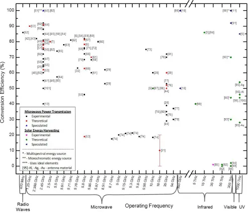
FIG. 8. Reported conversion efficiencies (as defined by their authors) at their maximum operating frequency of a rectenna device. Data points are grouped by the two applications of the rectenna - either Microwave Power Transmission or Solar Energy Harvesting, each displaying experimental, theoretical or speculated efficiency values. [**] indicates the reference corresponding to the data point. Data collected from [3,5–8,10,11,13,25,28,29,31,32,41–101]
and absorb broadband solar radiation which ranges from about 150 to 1000 THz, 85% of which corresponds to a wavelength of between 0.4µm to 1.6µm5. To reach the targeted frequencies in the high THz region, SBD rectifiers would not meet the criteria as the best cut-off frequencies are only up to a few terahertz103. MIM diodes are used for their potential to work in the higher THz region. The first practical demonstration was done by NIST85 who used atomic layer deposition grown Cr/CrOx/Au diodes coupled to a dipole antenna and measured its efficiency at 30 THz (achieved using a CO2 laser) to be below 1%. This attempt was carried
out on an un-optimised antenna structure with a poor MIM diode. Following this, numerous theoretical models have been proposed, predicting the overall conversion efficiency of the solar rectenna (see Figure8). For MPT rectennas, most theoretical and experimental efficiency results tend to be of the same order, whereas it can be seen that for Solar rectennas different attempts on modelling the performance predict a spread of efficien-cies. Some approaches are close to the Landsberg limit of 93.3%102 whilst others predict discouraging figures below 1% (Figure8).
theoretically derived89,92,94 employing various assump-tions and a variation of modelling approaches (Figure8). Mashaal & Gordon89 analysed the efficiency in terms of losses by the state-of-art rectenna designs which adopt single polarization antennas able to convert only half of the random-polarization input power from solar radiation and a half-wave rectifier blocking the negative voltages of the input signal. Their assumptions were based on ideal matching between antenna and rectifier, zero turn-on voltage, limitless switching speeds and non-filtered signal output from the antenna prior to entering the rectifier which yielded an overall conversion efficiency of 0.0795% and four times as high if a full-wave rectifier is employed. It is a common misperception that with rectennas, the diode forms a half-wave rectifier, which would hold true for a single diode in a series configura-tion. However, common rectenna design incorporates a diode connected in parallel, which forms a clamp circuit capable of rectifying the full wave99,100. Therefore, estimating rectenna conversion efficiency should not be discouraged by assuming a half-wave rectification mechanism. Instead, efforts should be concentrated in understanding the effect of impedance mismatch. Briones et al.92 based their model on the assumption that the collection of EM radiation by the antenna is done efficiently, which resulted in 0.001% efficiency of the system due to impedance mismatch losses between antenna and rectifier and inefficient rectification of the signal. By assuming efficient rectifier performance, the potential efficiency rises to approximately 1%.
An equally important criterion for efficient device operation is antenna material selection. Vandenbosch & Ma divided the analysis on the efficiency of nano-rectennas into two parts – 1) the efficiency by which the light is captured by the antenna and brought to its terminals97 and 2) the efficiency by which the captured light is transformed to low frequency power by the diode95,96. Considering first the antenna efficiency, they studied various antenna materials in the form of 250 nm dipoles placed on a substrate97. Their calculations predicted antenna efficiency of 61.6% for Ag, 50.3% for Al, 34.3% for Au, 29.5% for Cu and 9.4% for Cr. In a later paper, [95], they looked at the diode efficiency and more specifically, investigated the power loss due to impedance matching whilst assuming efficient signal rectification. This analysis was only done on the highest performing materials – Ag, Al and Au. Their work was a continuation of a previous work by Sarehraz et al.96, however their analysis covered 75% of the power radiated by the sun (up to 1000 THz) whereas Sarehraz
et al. only based their analysis on 15% of the spectrum. Although Al gave the best matching efficiency of 97%, the best overall conversion efficiency of the rectenna considering both constituent parts is with Ag which gives 54% whereas Al would have 46% and Au just 28%95(Figure 8). So far the analysed publications all share a united opinion that a suitable rectifier is needed in order for the above mentioned efficiency estimates
to be achieved or improved. For impedence matching, Ma & Vandenbosch95 suggest that the impedance of the rectifier must be of the order of 100Ω both for the real and imaginary part and favour aluminium as being a suitable material for this application.
A governing factor in rectifier performance is its RC time constant which defines the cut-off frequency, fc. This is the upper limit at which the rectification process is efficient. Above the cut-off frequency, rectification is still possible however the strength of the rectified signal at the output of the MIM will drop by a factor of approximately (fc)2, thus the higher the frequency above fc the lower the rectification efficiency96. The cut-off frequency is estimated by the following expression proposed by Sanchezet al.104,
fc = 1
2πRC (2)
where R is the series resistance and C is the capacitance. The cut-off frequency of the whole rectenna device can be evaluated by the following relation, which considers the antenna impedance (RA) and diode resistance (RD)92,
fc=
RA+RD 2πRARDCD
(3)
To achieve a high cut-off frequency, the RC constant must be small, which can be obtained with a small junc-tion area104, and appropriate material selection and fab-rication. MIM rectifiers, although the most promising rectifier technology, have not been demonstrated at high THz frequencies with the best MIM diodes operating only up to 150 THz (λ= 2 µm)5 (more detail in Section V). Improving MIM fabrication technology and material sys-tem design would potentially yield the solution to the rectenna efficiency.
So far, the reviewed efficiencies were all based on clas-sical approaches, not concerning thermodynamic limits to solar energy conversion. In terms of equilibrium, an antenna receiving power from any source and transferring it to the load must transmit the same amount of power back to the source3. If the power is extracted from the load, the reduction in its temperature will introduce a different approach to analysing the energy balance be-tween the incoming, extracted and reradiated powers. In this case, Corkish et al.3 state that the system would have the same conversion efficiency limit as the one ex-pected for a solar thermal collector. Assuming the Sun to be a 6000 K black body and the surroundings to be at 300 K, this limit is 85.4% for mono-spectral energy conversion and 86.8% for multi-spectral. Further analy-sis suggests that the Landsberg102limit of 93.3% can be reached due to certain benefits that the rectifying diodes have in rectennas (see [3] for more details), however this is hard to justify due to the generation of thermal noise by the rectifiers. Diodes cannot rectify their own ther-mal noise as it violates the second law of thermodynamics (known as Brillouin’s paradox106).
for the open circuit voltage and conversion efficiency of a rectenna with the rectification process based on the geometric property of the antenna tip which pro-vides a connection to the circuit and creates a tunnel junction. They envisioned the possibility of using ad-vanced nanofabrication techniques and a selective atomic layer deposition process to manufacture nanometer junc-tions which would potentially allow for rectification of blue light frequencies93. In modelling the circuit of the rectenna, it can either be considered as a constant volt-age source with an emf independent of the load resis-tance or as a constant current source whose emf depends on the load resistance. As suggested by Lerner et al.93, the rectenna device is more appropriately modelled as a constant current source in which case efficiencies are pre-dicted in excess of 70% for a monochromatic light source and an optimised device. Should the device be tuned for multiphoton absorption, the efficiencies are expected to be further enhanced93. The question remains as to whether a suitable technology is yet available to make such structures.
Another analysis on the broadband blackbody radia-tion response of optical rectennas was done by Joshi & Moddel90 by using the theory of photon assisted tun-nelling. By assuming negligible reverse current of the diode, zero dark current turn-on voltage and perfect matching to the antenna, the device power conversion efficiency at monochromatic light can approach 100%, whereas for multispectral light the value is approaching a maximum at 44% at an operating voltage of 1.1 V. It should be noted that these authors also suggest that spectral splitting is likely to improve the efficiency. This can be achieved by setting the operating voltage for each rectenna to rectify the desired spectral range, thus imply-ing that the operatimply-ing voltage for the diodes in rectennas has a similar role to the band-gap as a limiting factor in photovoltaic devices90.
With its proven success to receive and rectify monochromatic microwave beams with high efficiency, there is a growing interest in establishing the true poten-tial of the rectennas’ ability to convert solar radiation. As seen in Figure 8, there are many theoretical approaches predicting this, however there is no one universal theory that clearly states whether the solar rectenna can com-pete with, let alone surpass common photovoltaic cells. There is however, the common opinion between scien-tists worldwide that the technology is not mature enough to fabricate a device of comparable efficiency. Advances in antenna engineering suggest that it is now possible to manufacture nano sized antennas which can absorb solar radiation from the infrared to the visible frequen-cies (Section IV). Work on the rectifier component has seen great progress over the years with many attempts showing great potential for use in rectenna devices (Sec-tionV).
IV. ANTENNA
Antennas are used either as transmitters, to create electromagnetic (EM) waves that have a well-defined ra-diation pattern, or as receivers of EM waves from a re-mote source86. The purpose is usually to send or extract information that is encoded into the EM wave. Anten-nas are now essential in many aspects of modern day living, the mobile phone being the most common exam-ple. They normally operate at a resonance. Typically this is a half wavelength dipole antenna. The resonant wavelength of the antenna will be at the wavelength of the incoming propagating signal and energy is then trans-ferred between them. For this reason, the antennas are usually fabricated in the dimensions of the wavelength of the incident wave. A higher frequency thus requires a smaller antenna. However, an antenna designed to be resonant at a very specific frequency by only considering a linear dimension does not guarantee efficient energy ab-sorption. Other factors such as impedance mismatch in the circuits, bandwidth, direction and polarisation of in-cidence radiation needs to be considered. The aim of this section is to introduce some different designs of antennas for microwave and optical frequencies.
Most antennas at microwave frequencies are designed to work within a specific frequency band reserved for industrial, scientific and medical (ISM) frequency use. For example, one of the most popular frequency bands is 2.4 – 2.5 GHz, which devices such as wireless networks, near-field communications, and Bluetooth use. There-fore these antennas only require millimeter dimension. A dipole antenna is one of the simplest designs. It con-sists of two identical metal elements in mirror symmetry. The most common form is two metal rods aligned on the same axis. The length of the metal rods is half the size of the resonance wavelength. Higher-order resonance modes also occur in the same antenna but at reduced efficiency due to attenuation of the induced current in the antenna. Nevertheless, the accepted frequency bandwidth is very narrow. A slight variation of the incoming frequency gives rise to parasitic capacitance and inductance result-ing in inefficient energy absorption. Therefore, a precise fabrication of the antenna is necessary. This increases the difficulty in manufacturing good devices, especially when the frequency of interest is higher.
FIG. 9. SEM images of (left) bow-tie antenna with integrated Ni-NiO-Ni diode and (right) spiral antenna. (Reprinted from [108], c1998 with permission from Elsevier)
As previously discussed in Section III, at microwave frequencies, antennas can be designed to be very efficient. Achieving such high efficiencies at the higher frequencies is more challenging with scaling down antennas. The so-lar spectrum emits energy across a broad band, which implies that the antenna must absorb a large bandwidth of solar frequency, otherwise most energy will be lost. For an antenna to operate efficiently at optical frequen-cies it is necessary to adjust both the inductance (L) and capacitance (C) to bring the device resonance to the required short wavelength. This would require both L and C to be very small113. To achieve this, the dimen-sions of the antenna must be reduced to the scale of the optical wavelength, i.e. nanometer. Scaling down the conventional antenna design to nanometer is of interest, as it can be determined whether classical antenna theory remains valid. For example, electron beam lithography has been used to fabricate a dipole antenna with a 3.5 nm NiO layer, sputtered between the two Ni antenna arms109. The dipole antenna had a total length of 6.7 µm and was designed for 10 µm wavelength (30 THz). Another example is of a gold dipole antenna fabricated by using focus ion beam (FIB) milling114.
These attempts have proven it impossible to scale clas-sical antenna designs to the optical frequency regime. At radio frequency the metals used for the construction of antennas can be considered almost lossless. This allows a large variation of radio frequency antennas to be designed by considering the metal to be a perfect conductor. How-ever, the losses become increasingly significant as the fre-quency rises. This is due to the finite effective mass of electrons causing the electrons to react with increasing phase lag to an oscillating EM field115. As soon as the phase lag approaches 90othe amplitude of the charge os-cillation goes through a maximum and is only limited by the Ohmic and radiation damping of the system116. In metallic nanoparticles this resonance corresponds to the localized surface plasmon resonance (LSPR). For gold, silver, aluminium and copper the LSPR is in, or very close to the visible light part of the spectrum. The LSPR can be exploited to overcome some of the draw-backs of antennas at optical frequency, in particular the high Ohmic losses compared to microwave frequencies.
A. Properties of Metals at Optical Frequencies
The optical response of metals can be described by a complex frequency-dependent dielectric function,
(ω) =1(ω) +i2(ω) (4)
The electric field is related to the induced polarization density as117,
P(ω) =0[(ω)−1]E(ω) (5)
For optical antennas, Ohmic losses in the metal should be minimized. The Ohmic absorption is proportional to the conductivity of the material, σ(ω), which is related to the dielectric function by.
2=σ(ω)/0ω (6)
Ohmic losses take place in close proximity to the surface of the metal, within the so-called penetration depth118, which for metals at visible wavelengths are of the or-der of several nanometers (approximately 13 nm and 31 nm for aluminium and gold at 620 nm wavelength, respectively)119. The dielectric properties of a metal can cause a LSPR in the visible spectrum, which is connected to large local fields, and enhanced scattering and absorp-tion.
At optical frequencies the metal conduction electrons may be treated as an ideal electron gas. The collective behaviour of this free electron gas can be expressed using the Drude-Sommerfield model118,
(ω) =∞− ω2
p
ω2+iγω (7)
where ωp is the volume plasma frequency and γ is a damping constant118. (For Au at optical frequencies ωp= 13.8×10¹⁵s−1 andγ= 1.07×10¹⁴s−1)116
The DrudeSommerfield model does not account for in-terband transitions due to photons with high-enough en-ergy promoting electrons from lower lying valence bands to higher energy conduction bands120. This can be de-scribed using a Lorentz model of the dielectric function, which is described by a collection of damped harmonic oscillators with well-defined resonance frequencies,ω0,
(ω) =∞+ n X
i=1
αiω2p
ω2
0i−ω2−iγiω
(8)
whereωp depends on the density of bound electrons in-volved in the absorption process andγis a damping con-stant for the bound electrons. This Lorentz model shows strong deviation from the free electron gas model near ω0, leading to a maximum in the imaginary part of(ω)
and strongly increased damping.
Cu are very similar, with a Drude-like response for wave-length above 600 nm and an onset of interband transi-tions occurring around 530–550 nm, making them excel-lent for antennas in the red and near-IR spectral region. For Ag the first interband transition is for a short wave-length, less than 400 nm, making it superior to Au for wavelengths around 500 nm. Al has a larger negative real part of dielectric function, and so among the four metals is the one that best approximates an ideal metal, especially in the 400–600 nm spectral region116. Unfor-tunately there is an interband absorption peak located at 800 nm wavelength, making Al unsuitable for use in the near-IR region, although, as previously discussed, it makes a good candidate for solar rectenna due to its high predicted matching efficiency95. As well as the spectral properties of the metals, the chemical stability also needs to be carefully considered. Ag and Cu are known to rapidly oxidise under ambient conditions and Al forms thin passivation layers of Al2O3. Due to its dielectric
functions in the red and near IR parts of the spectrum and its excellent chemical stability, Au is the material most often used as a nanoantenna.
B. Scattering and Absorption Properties of Optical Antennas
Radio frequency and microwave antennas will normally always be considered as circuit elements connected to a feeding circuit. At optical frequencies the circuit ele-ment models are not valid and so optical antennas often appear as isolated or electromagnetically coupled struc-tures, whose resonant properties have to be considered. Here, the LSPR of single and coupled metal nanoparti-cles, specifically the absorption and scattering properties, are considered. Consider a monochromatic plane wave of irradianceIi incident on a sphere of radiusa. If the ir-radiance is multiplied by a cross-section then the power absorbed or scattered by the particle can be calculated,
Pabs =Ii.Cabs (9)
Psca =Ii.Csca (10)
where Cabs and Csca are the absorption and scattering cross-sections, respectively. The cross-sectional areas can be normalized to the cross-section of the sphere to give the scattering and absorption efficiencies:
Qabs = Cabs
πa2 (11)
Qsca = Csca
πa2 (12)
whereais the radius of the sphere. Equations11and12
define the two loss mechanisms, Qsca which is radiative andQabs, which is non-radiative, the extinction efficiency
being the sum of both these terms.
Smaller sized particles restrict electron motion and cause electrons to collide with the inner surface of the particle, resulting in loss of energy and increased absorp-tion. Absorption is therefore the greater loss mechanism in smaller particles. The radiation damping rate is pro-portional to the number of electrons. This means that the larger the particle, the more significant this factor and the broader the plasmon resonance becomes. A larger particle volume results in a decrease in the amount of in-cident radiation absorbed but an increase in the scatter-ing. Scattering and absorption due to small spheres can be described using the well-known Mie theory121, where
Cabs= 2πn1
λo
Im(α) (13)
Csca=
2πn1
λo
4 |α|2
6π (14)
The polarization,α, is given by:
α=r3 (2−1) (2+ 21)
(15)
wherer is the radius of the sphere, 2 the complex
per-mittivity of the sphere and1the complex permittivity of
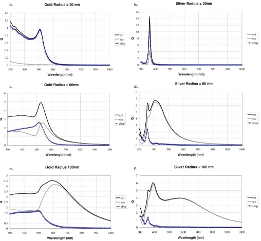
the surrounding medium. Examples of Mie theory calcu-lations of extinction, scattering and absorption for gold and silver spheres of various radii are shown in Figure10. Interesting observations that arise from the Mie theory calculations are that a number of peaks can be observed for larger diameter spheres, the longest wavelength peak being a dipole mode. As expected the LSPR broadens as the particle size increases but absorption and scatter-ing maximums are not always at the same wavelength. The absorption and scattering properties can be tuned using different shaped particles. In this case more com-plex calculation methods are required, for example the Discrete Dipole Approximation (DDA)123, Finite Ele-ment Method (FEM)124or Finite Different Time Domain (FDTD)125. FDTD is a popular method since it is pos-sible to consider the scattering and absorption from any shaped particle in any dielectric environment and since the calculation is in the time domain a single calculation will yield the spectral response over a wide bandwidth, using a Fourier Transform126.
If a surface that fully encloses the scattering object is now defined, then by considering the total field flowing through it, one can calculate the normalized absorption cross-sectionQabs from127,
Qabs= R s
Re(0.5E×H∗)da
|Si|
(16)
and by considering the scattered field the normalised scattering cross-section,Qsca, is found from127,
Qsca =
−R
s
Re(0.5Es×H∗s)da
|Si|
FIG. 10. Mie calculations of extinction, scattering and absorption efficiencies for silver and gold nanospheres (a) Au sphere of 20 nm radius (b) Ag sphere of 20 nm radius (c) Au sphere of 60 nm radius (d) Ag sphere of 60 nm radius (e) Au sphere of 100 nm radius (f) Ag sphere of 100 nm radius.
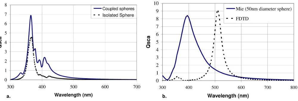
where |Si| is the power incident on the cross-sectional area of the nanoantenna. Using computational electro-magnetics to calculate the electric (E) and magnetic (H) fields at the enclosing surface, Equations 16and 17can be solved. Figure 11 shows the Qsca calculated using FDTD for (a) two closely spaced and (b) two overlap-ping spheres, where the spheres are silver and of 50 nm diameter122.
Furthermore, the surrounding dielectric environment and orientation of the nanoparticle can significantly mod-ify the absorption and scattering properties127. As an
FIG. 11. FDTD calculations ofQscafor (a) two closely coupled Ag spheres and (b) two overlapping Ag spheres.
FIG. 12. Depiction of the two configurations considered: (a) nanoparticle extending into air and (b) nanoparticle extend-ing into silicon. (Reprinted from [127])
case (a) it is the absorption that is the largest extinction component.
We have discussed the LSPR of isolated and coupled nanoparticles in terms of their absorption and scatter-ing efficiencies. The subsequent coupling between the nanoantenna and rectifying diode will need to be opti-mised. Absorption is caused by the generation and re-combination of electron hole pairs (EHP). EHP formation occurs when the plasmon quantum excites an electron from the Fermi level to an occupied state below the vac-uum level. It has been shown that the concentrated elec-tric fields around a nanoantenna, due to the LSPR, can cause hot electron carriers128–130. Because of their higher energy, hot electrons will extend further away from the nanoparticle than an equilibrium electron distribution, which is above the vacuum level. If a nearby electron
ac-ceptor is present, hot electrons can transfer into its elec-tronic states. This hot electron carrier generation and injection into an acceptor due to the high fields is a topic of much current research in photovoltaic devices128–131, in particular optimizing the efficiency of this process.
For an optical rectenna it is desirable to enhance and localize (i.e. concentrate) the propagating fields to enable coupling into external circuit elements. The concentrated fields tend to be higher for particles with a higher scat-tering efficiency and between the small gaps of coupled nanoparticles. This is opposite to hot electron devices which seek to maximise the absorption of photons in the nanoparticle. Figure14shows the values of electric field, normalized to the incident field, around Ag nanoparticles, formed by colloidal lithography using 500 nm polystyrene spheres as a template on a glass substrate132(this makes the triangular sides around 120 nm in this case). The scale is logarithmic and it can be seen that there are up to two orders of magnitude electric field enhancement in the gaps between the particles.
C. Alternative structures
[image:15.612.53.299.302.452.2]FIG. 13. QscaandQabsFDTD calculations for (a)
nanoparti-cle extending into air (b) nanopartinanoparti-cle extending into silicon. (Reprinted from [127])
the antenna length can be greatly reduced while provide a mechanical bandwidth of 4.4 GHz.
The propagation wavelength for the waveguide in the material is very small. This suggests that if the an-tenna is very close to the diode, it can reduce losses116. In Travelling Wave (TW) MIM rectenna design, a MIM junction is created between the top and bottom bow-tie antenna134,178(Figure16a). This allows the diode to rec-tify the absorbed radiation at this MIM junction. This design is similar to a bow-tie antenna, except that the left bow and the right bow are separated by a very thin layer of insulator, forming an extended MIM tunnelling diode. The absorbed radiation excites surface plasmon and propagates along this axis (Figure16c). The current induced between the top metal and bottom metal cause tunneling of electrons to occur. A final rectified current is produced due to the asymmetry in the IV characteristic at the bias point (further information in SectionV). One of the advantage in this design is that it is not limited by theRC bandwidth.
[image:16.612.317.554.60.245.2]FIG. 14. Concentrated electric field calculations around trian-gular like nanoparticles of height 100 nm formed by colloidal lithography with 500 nm polystyrene spheres. The excitation wavelength is 780 nm and calculations were carried out using FDTD. (Reprinted from [132])
FIG. 15. (a) 3D schematic diagram of the optomechani-cal nanoantenna investigated. A near-field intensity map of the device is shown on top. (b) Simulated optical force and Casimir force (inset) on the suspended beam as a function of gap width. (c) Simulated (a) transmission and (b) reflection power spectrums versus gap width. (e) Nanocircuit lump ele-ments model. (Reprinted from [133], c2012 with permission from Optical Society of America)
Another example of integrated rectenna design is the slot-antenna-based frequency selective surface (FSS) with integrated MOM diode135. The materials consists of Al, Al2O3 and Pt on benzocyclobutene (BCB) standoff,
[image:16.612.317.561.342.528.2]radi-ation is parallel to the diode junction, the electric field is concentrated 2000 times across the diode with a decrease of reflectance around the desired wavelength, which can be used as an indication of absorption. A working device was fabricated with e-beam lithography (Figure17) and similar optical response in reflectance was measured.
[image:17.612.55.299.132.359.2]FIG. 16. (a) Isometric view of the antenna-coupled TW de-vice. Instead of crossing over as in a typical bow tie antenna in figure 1, the antenna arms converge into a parallel-plate waveguide with a 2 nm thin insulator between the metal M1 and M2. (b) Circuit representing the TW MIM device. (c) 3D view of the TW MIM diode. (Reprinted from [134], c2010 IEEE. Reprinted, with permission, from IEEE)
FIG. 17. SEM images of fabricated MOM diode-coupled frequency selective surface device.(a) Image of entire ar-ray consisting of 16,800 diode-coupled elements is less than 0.325 mm2, (b) closer image of the array showing several
pieces of metal coated photoresist that became attached to the sample after lift-off, and (c) diode of working device (Reprinted from [135], c2012 with permission from John Wi-ley & Sons)
The recent development of graphene technology also prompts the incorporation of graphene into nanoantenna
design. Ag is known to suffer from sulfidation under am-bient environment, resulting in degradation of the plas-monic property136. Graphene was shown to be able to passivate the Ag and prevent sulfidation without affect-ing the plasmonic property of the Ag nanoantenna136. Additionally, radical changes in the plasmon energy and strength were also observed by electrically doping pat-terned graphene arrays with a gate voltage137. The de-velopment of new materials such as graphene open up new possibility to design a better optical antenna.
D. Impedance matching
[image:17.612.373.506.443.543.2]As previously introduced, the efficient energy trans-fer from antenna to diode requires an impedance match between both components. A theoretical analysis on an optical dipole nanoantenna showed that the nanoantenna appears to be an effective RLC parallel circuit138 (Fig-ure18). The two parallel resistances are due to radiative decay and non-radiative decay rates. The electrical prop-erties of a nanoantenna are intrinsically influenced by the material used, dimensions and geometric shape95. Dipole antennas of length between 100 and 350 nm for Ag, Al, and Au on glass have been studied through simulation95, as previously introduced. At a single frequency and as-suming no loss of power in impedance mismatch, a silver dipole shows the highest efficiency. However, the upper bound efficiency drops when the solar irradiance spec-trum is taken into account. Further investigation by in-clusion of losses due to impedance mismatching showed even further decrease in conversion efficiency (see Sec-tionIII).
FIG. 18. Equivalent circuit of a metallic nanoantenna. (Reprinted (Fig. 1) with permission from [138], c2010 by the American Physical Society)
Liu et al.139 considered the nanoantenna as lumped elements in three-dimensional nanocircuits and demon-strated that impedance of the antenna can be tuned by loading a dielectric or a metal in the gap between a dimer. A SiO2 load was used as the dielectric material. In the
[image:17.612.54.300.478.583.2]capacitors. To develop the idea further, a combined gold-SiO2 load was also fabricated. The circuit now
corre-sponds to an LC parallel circuit in series. In all cases, the impedance was tunable by changing the dimensions and the materials of the load, with the gold-SiO2showing
largest tunability.
E. Nanofabrication
For microwave energy extraction device dimensions are in the micrometre range, achievable using well estab-lished photolithography techniques. At infrared and op-tical frequencies nanometre dimensions are required. Un-fortunately the resolution of photolithography is limited by the diffraction wavelength of light and so different fab-rication techniques are required. Fabfab-rication techniques that have been demonstrated to be effective at obtain-ing nanometre resolution are electron beam lithography, nano-imprint lithography and colloidal lithography.
FIG. 19. (a) Photograph of a single layer negative index ma-terial (NIM) sample and (b) transfer printed gold grating on a flexible foil. Top-view SEM images of (c) the single func-tional fishnet layer and (d) the Swiss-cross NIMs fabricated using nanoimprint technology. (Reprinted from [141], cIOP Publishing. Reproduced by permission of IOP Publishing. All rights reserved.)
Electron beam lithography is similar to photolithog-raphy but uses an electron beam instead of light. The wavelength of the electron beam is much smaller than light, allowing sub-10 nm resolution in patterning and creation of well-defined structure such as the nanogap in antenna-coupled diode in Figure 18. However it is costly and cannot be effectively up scaled for a large area. Nanoimprint lithography uses a pre-made mask to create a pattern on a substrate140. This mask can be used nu-merous times and allows large area fabrication. Com-pared to e-beam lithography, nanoimprint lithography enables large area patterning but each mask is specially designed for a specific nanostructure. Figure 19
[image:18.612.318.566.212.385.2]illus-trates an example of a large area of nanostructures fab-ricated using nanoimprint technology. A new mask will have to be made if the nanostructure required is different and the cost of the mask is high. Nanosphere lithography is a more versatile lithography technique, based on self-assembly of nanospheres. It allows fabrication of large area devices at relatively low cost. Although it does not allow huge degree of manipulation in the shape of nanostructure compared to e-beam lithography, a vari-ety of shapes in large ordered array has been fabricated successfully (Figure20), such as nanotriangles132,142,143, crescent moon144, nanorings144, nanocones145, and three-dimensional structures146.
FIG. 20. SEM images of variety of gold nanostructures based on nanosphere lithography technique (a) nanotriangles, (b) slanted nanocones, (c) nanodisc array, (d) nanoholes. (Note: 500 nm scale bar in all images)
Advances in nanofabrication techniques are crucial in developing a better nanoantenna. Further details on nanoantenna theory and application can be found in some recent reviews [116,147].
V. RECTIFIER
[image:18.612.66.286.296.464.2]parameters have been defined5,149,185,188, which, if satis-fied, result in characterising a device as a diode rectifier:
fasym(V) =
IF(V) IR(V)
; Asymmetry>1 (18)
fN L(V) = dI dV(V)/
I(V)
V ; Nonlinearity>3 (19)
fRES(V) = d2I d2V(V)/
dI
dV (V);Responsivity>7V −1
(20) These three Figures of Merit (FOM) are commonly used to characterise the performance of MIM devices however can be equally applied to other diodes. The asymme-try FOM, defined in Equation 18, is the absolute ratio of forward to reverse current at a bias, a value of 1 in-dicating full symmetry and hence no rectification. The non-linearity FOM, as defined by Equation19, is the ra-tio of the differential conductance to the conductance and is a measure of the deviation from a linear resistor. Fi-nally the responsivity FOM defined in Equation20is the ratio of the second derivative of the I-V curve and the differential conductance and is a measure of the rectified signal as a function of input power. It is essential that the diode in a rectenna exceeds all of these criteria as the higher the FOMs for the diode, the more efficient the rectification process.
note: There was some disagreement argued by Tucker & Feldman150 that responsivity should be described
us-ing second-difference equations and not derivatives in or-der to unor-derstand high frequency rectification. However, proving which is the correct approach is beyond the scope of this review as the authors aimed to only bring this the-ory to the attention of readers. The authors support the use of derivatives of the I-V curve in analysis of these FOMs.
The fundamental operational theory and recent exper-imental and theoretical developments of Schottky bar-rier diodes (used in the microwave power transmission rectenna), metal and metal-insulator-insulator-metal diodes (proposed for solar rectenna), and geometric diodes (proposed for solar rectenna) will be re-viewed in this chapter.
A. Schottky Barrier Diodes
Schottky barriers have been used as rectifying devices since the first cat’s whisker detectors in the first decade of the 20th century. The ‘barrier’ itself is formed within the semiconductor side of a metal-semiconductor (MS) interface, the result of its conduction and valence bands bending to align the Fermi levels of each material. Fig-ure 21 shows an ideal MS interface with the Schottky barrier, Φ0B,n, marked.
[image:19.612.321.561.53.241.2]In Figure 21, note that within the semiconductor, a
FIG. 21. Band diagram of an ideal Schottky Barrier, Φ0
B,n,
contact formed with n-type semiconductor with an applied bias, Va. (Reprinted from [151], c2001 with permission from
Elsevier)
depletion region, or space charge region, forms. This is a region of the semiconductor that is devoid of mobile charge carriers when the device is unbiased, and as such it can be considered as the dielectric between two plates of a capacitor, so having a direct influence on the RC time constant. Minimising the capacitance of a Schottky diode can be achieved through scaling (though this has the equal and opposite effect on the diode’s resistance), or by increasing the depletion region width by using low semiconductor doping.
The full operation of a diode has been well studied and understood over the past century, and readers are re-ferred to [152,154], for a basic understanding of Schottky diode formation, operation and physics under different biasing conditions. Both the forward and reverse current-voltage (I-V) relationship is in most cases, where semi-conductor doping is low enough, dictated by thermionic emission, rather than recombination or tunneling. The equation for thermionic emission, where the carrier in the semiconductor must pass up and over the potential barrier into the metal, is classically expressed as152–154,
I=AA∗T2exp −βΦ0B,n[exp (βVA/η)−1] (21)
whereArepresents the contact area,A∗is the Richardson constant, T is the temperature, VA is the applied volt-age,ηthe ideality factor andβ=q/kbT, withqthe elec-tron charge, andkb the Boltzmann constant. However, built into Equation 21 is the presumption that a per-fect, homogeneous interface exists, with just one uniform value of Φ0
pro-vide a much more rigorous understanding of the Schot-tky diode and its operation under this inhomogeneous regime. Given the small potential size of a Schottky rectenna, the impact of such interface inhomogeneity will be the source of significant device-device variation, and an unpredictability of cut-off frequencies.
Typical Schottky diodes can have good diode char-acteristics in terms of the FOMs mentioned in Equa-tions18, 19 and 20, as demonstrated by the simple ex-ample of a Cr/Si Schottky diode made in-house for [155]. The characteristics of this diode are close to ideal (i.e. η < 1.1), and its FOM values are strong, with a diode asymmetry of 1669, nonlinearity of approximately 0.2 and responsivity above 10 V−1. However, high series
[image:20.612.317.559.251.382.2]resistance and depletion region capacitance result in a cut-off frequency of just 40 GHz. Therefore, this is a de-vice which could be suitable in a microwave power trans-mission rectenna, but it would be entirely ineffectual at solar frequencies.
FIG. 22. Room temperature Current-Voltage characteristics of a simple Cr/n-Si lateral type Schottky barier diode of area 0.448mm3. SBH calculated at 0.51eV, ideality factor of 1.06,
diode asymmetry at±0.25V of 1669, nonlinearity estimated at 0.2 and responsivity above 10V−1. The cut-off frequency has been estimated at 40 GHz.
With appropriate device design in terms of size and interface homogeneity, parasitic capacitances and resis-tances, arising from skin effects and residual native oxide scales at the MS interface, can be minimised to have a significant effect on the RC time constant. In silicon the cut-off frequency has been seen to reach 1 THz ob-tained by a layer of Ti-Pt-Au on a thin layer of n-Si161, whereas 400 GHz has been seen from a simple Ti/n-Si structure162. On GaAs, frequencies of up to 5 THz have been achieved, as reviewed by Sizov & Rogalski163. This is obtained using highly doped GaAs substrate with an Ohmic contact on the back side upon which a thin (0.3-1 µm) epitaxial GaAs layer is grown, with Pt forming the Schottky contact. A honeycomb diode chip design
enables thousands of diodes (diameters of 0.25-1µm) on a single chip whilst minimising parasitic losses.
As rectifiers in the wireless power transmission rectenna application, SBDs are more than suitable can-didates and as seen in SectionIIIcan operate efficiently. With cut-off frequencies in the low THz, Schottky diodes may potentially find usage as infrared rectennas although they will be limited to only function at a fraction of the far-infrared range, where the incident solar radia-tion is only up to 0.3 W/m2/nm. The aim is to have
solar rectennas operating at the high THz region where solar radiation is up to 1.7W/m2/nm, however Schot-tky diodes will not be able to efficiently rectify such high signals. Therefore, other approaches such as the MIM/MIIM and geometric diodes are being considered for the solar rectenna.
FIG. 23. Schottky diode as the active component for the solar rectenna device - concept inspired by Knightet al. Ashowing a band diagram of the proposed photocurrent mechanism,B
showing the device layout and structure andC showing an SEM image of the array of devices. (Reprinted from [94],
c
2011 with permission from The American Association for the Advancement of Science)
[image:20.612.57.295.284.464.2]would require the conversion efficiency to be increased, though with the current state-of-art, this seems improb-able.
B. Metal-Insulator-Metal Diodes
Current transport in Metal-Insulator-Metal (MIM) diodes is due to quantum electron tunnelling through an ultra-thin insulator layer (typically<10 nm165). Recti-fication in these devices is due to variation in tunnelling rates caused by barrier asymmetry due to material selec-tion, device geometry, thermal asymmetry, and photon induced deviation in electron flux distribution across oc-cupied and unococ-cupied states105, all contributing towards a nonlinear asymmetric I-V response. In the current re-view, we will qualitatively explain the nature of the I-V asymmetry taking into account the material selection for planar MIM devices under no illumination and thermal equilibrium. Under illumination, electron tunnelling is stimulated by different processes depending whether an antenna is or is not coupled to the diode. Further reading is suggested in [105,165,166,169]. Thermionic emission also contributes to tunnel diodes’ I-V curves165,188,189, especially to devices with thick insulating layers188.
1. Theory of operation
Consider a Metal-Insulator-Metal junction as shown in Figure 24a. Metal 1 has a workfunction, Φ1, lower
than that of Metal 2, Φ2, and χ is the electron
affin-ity of the Insulator. The barrier height at the metal-insulator interface is determined from the difference be-tween the workfunction and electron affinity respectively. At zero bias the band structure is shown in Figure24a. By applying a negative bias (Reverse bias) to Metal 1, the band diagram shifts as in Figure 24b. In this case direct tunnelling is observed as a result of the effective
tunnelling distance,dt, being the same length as the insu-lator thickness. Further increasing the applied voltage, VA, decreases the effective dt, and it becomes shorter than the length of the insulator (as seen in Figure24c). In this case, Fowler-Nordheim tunnelling167 starts to oc-cur. When a bias of the same magnitude is applied to Metal 2 (Forward biasing), the bands shift as in Fig-ure24d. Fowler-Nordheim tunnelling is observed in this case and occurs at a lower voltage, the higher the bar-rier asymmetry at both metal-insulator interfaces (aris-ing from the difference in metal workfunctions). Further increasing the reverse bias (as in Figure24e) will further decrease the effective tunnelling distance, dt, which fur-ther increases the tunnelling probability in forward bias. Therefore, rectificaton occurs because for the same volt-age magnitude in forward bias, dt will be shorter and more current will be flowing than in the equivalent case in reverse bias. By changing the applied voltage, the tun-nel distance changes linearly and the tuntun-nel current is
ex-FIG. 24. Ideal band diagram for a MIM diode with dissim-ilar workfunctions for Metal 1, Φ1, and Metal 2, Φ2,χ the
Insulator’s electron affinity, EF the Fermi level,dtthe tunnel
distance andVA the applied voltage. a. No bias situation
(VA= 0V);b. &c. Negative bias at Metal 1 (Reverse bias);
[image:21.612.350.525.52.615.2]![FIG. 2. Block diagram of solar rectenna and load. (Reprintedfrom [9], c⃝IOP Publishing](https://thumb-us.123doks.com/thumbv2/123dok_us/9537521.458691/3.612.56.294.394.523/fig-block-diagram-solar-rectenna-load-reprintedfrom-publishing.webp)


![FIG. 13. Qsca and Qabs FDTD calculations for (a) nanoparti-cle extending into air (b) nanoparticle extending into silicon.(Reprinted from [127])](https://thumb-us.123doks.com/thumbv2/123dok_us/9537521.458691/16.612.317.561.342.528/qsca-calculations-nanoparti-extending-nanoparticle-extending-silicon-reprinted.webp)
