memory accesses, execution time and energy consumption
.
White Rose Research Online URL for this paper:
http://eprints.whiterose.ac.uk/149053/
Version: Accepted Version
Article:
Kelefouras, V and Djemame, K orcid.org/0000-0001-5811-5263 (2019) A methodology
correlating code optimizations with data memory accesses, execution time and energy
consumption. Journal of Supercomputing, 75 (10). pp. 6710-6745. ISSN 0920-8542
https://doi.org/10.1007/s11227-019-02880-z
© 2019, Springer Science+Business Media, LLC, part of Springer Nature. This is an author
produced version of an article published in Journal of Supercomputing. Uploaded in
accordance with the publisher's self-archiving policy.
[email protected] https://eprints.whiterose.ac.uk/ Reuse
Items deposited in White Rose Research Online are protected by copyright, with all rights reserved unless indicated otherwise. They may be downloaded and/or printed for private study, or other acts as permitted by national copyright laws. The publisher or other rights holders may allow further reproduction and re-use of the full text version. This is indicated by the licence information on the White Rose Research Online record for the item.
Takedown
If you consider content in White Rose Research Online to be in breach of UK law, please notify us by
Noname manuscript No.
(will be inserted by the editor)
A methodology correlating code optimizations with
data memory accesses, execution time and energy
consumption
Vasilios Kelefouras · Karim Djemame
Received: date / Accepted: date
Abstract The advent of data proliferation and electronic devices gets low
execution time and energy consumption software in the spotlight. The key to optimizing software is the correct choice, order as well as parameters of optimizations-transformations, that has remained an open problem in compi-lation research for decades for various reasons. First, most of the transforma-tions are interdependent and thus addressing them separately is not effective. Second, it is very hard to couple the transformation parameters to the pro-cessor architecture (e.g., cache size) and algorithm characteristics (e.g. data reuse); therefore compiler designers and researchers either do not take them into account at all or do it partly. Third, the exploration space, i.e., the set of all optimization configurations that have to be explored, is huge and thus searching is impractical.
In this paper, the above problems are addressed for data dominant affine loop kernels, delivering significant contributions. A novel methodology is pre-sented reducing the exploration space of six code optimizations by many orders of magnitude. The objective can be Execution Time (ET), Energy consump-tion (E) or the number of L1, L2 and main memory accesses. The exploraconsump-tion space is reduced in two phases. Firstly, by applying a novel register blocking algorithm and a novel loop tiling algorithm and secondly, by computing the maximum and minimum ET/E values for each optimization set.
The proposed methodology has been evaluated for both embedded and general purpose CPUs and for seven well known algorithms, achieving high memory access, speedup and energy consumption gain values (from 1.17 up to 40) over gcc compiler, hand written optimized code and Polly. The exploration space from which the near-optimum parameters are selected, is reduced from 17 up to 30 orders of magnitude.
Keywords code optimizations·data cache·register blocking·loop tiling ·
high performance·energy consumption·data reuse
1 Introduction
Although significant advances have been made in developing advanced com-piler optimization and code transformation frameworks, current comcom-pilers can-not compete with hand optimized code, especially for data dominant appli-cations; compilers lack of efficient register blocking and loop tiling algorithms which are the key to data dominant applications [9]. Writing efficient code is a hard and time consuming task as the correct choice, order as well as param-eters of optimizations for a specific code, are not efficient for another code, CPU or even for a different input size.
To tackle the above problems, researchers propose heuristics [27], em-pirical techniques [6], iterative compilation techniques [26], techniques that simultaneously optimize only two transformations, e.g., register allocation and instruction scheduling [49] and semi-automatic approaches such as Loopy [33], POET [45], ChiLL [13] and Orio [18], where the programmer specifies a loop transformation at a high level and it is then carried out automatically. The most promising automatic approach is iterative compilation where many dif-ferent versions of the program are generated-executed by applying a set of com-piler transformations, at all different combinations/sequences. However, itera-tive compilation is extremely expensive in terms of compilation time and there-fore researchers and current compilers try to reduce it by using i) both iterative compilation and machine learning compilation techniques [29] [5] [54] [38], ii) both iterative compilation and genetic algorithms [26], iii) heuristics and em-pirical methods [12], iv) both iterative compilation and statistical techniques [17], v) exhaustive search [25]. However, by employing these approaches, the remaining exploration space of code optimizations, i.e., the set of all opti-mization configurations that have to be explored (optiopti-mization sets), is still so large that searching is impractical. The end result is that seeking the opti-mal configuration is impractical even by using modern supercomputers. This is evidenced by the fact that most of the iterative compilation methods use either low compilation time transformations only or high compilation time transformations with partial applicability so as to keep the compilation time in a reasonable level [22] [46]. As a consequence, a very large number of solu-tions is not tested. This has led compiler researchers use exploration prediction models focusing on beneficial areas of optimization space [14].
Unlike existing approaches, our method reduces the exploration space of six code optimizations by many orders of magnitude and therefore it is practical to be searched; thus, the quality of the end result is significantly improved. The exploration space is reduced by i) taking into account the HardWare (HW) architecture details, data reuse and arrays’ data access patterns, ii) addressing several code optimizations together as one problem and not separately, as they are interdependent.
The main steps of our methodology1 are as follows.
1 This is an extension of the conference paper ”A methodology for efficient code
optimiza-tions and memory management”, ACM International Conference on Computing Frontiers 2018
First, the exploration space of code optimizations is reduced by providing an efficient register blocking and loop tiling algorithms; these two algorithms consist of a) loop unroll, scalar replacement, register allocation and b) loop tiling, array copying, transformations, respectively. A unified framework is proposed to orchestrate the aforementioned transformations, together as one problem; the transformations are tailored to the target CPU HW details, data reuse and data access patterns.
Afterwards, we provide formal methods describing a) the number of L1 data cache (L1dc), L2 cache (L2c) and Main Memory (MM), accesses and b) the number of arithmetical instructions, as a function of the aforementioned optimization sets, CPU details and algorithm’s input size.
Next, a Power consumption (P) model based on mcpat [30] simulator and an Execution Time (ET) model extending C-AMAT [56] [51], are developed, giving ETM AX, ETM IN and P (and as a consequence Energy Consumption
(E), as E = ET ×P), as a function of the number of L1dc, L2c and MM accesses and as a consequence to the aforementioned optimization sets, CPU HW details and algorithm input size. Given that the maximum and minimum values of ET/E are known for each optimization set, the exploration space can be further reduced.
The proposed methodology has resulted in five contributions.
– A new approach applying code transformations by taking into account the memory hierarchy HW architecture details and the application special memory access patterns
– A single framework addressing the aforementioned transformations to-gether as one problem and not separately
– Formal methods providing the number of memory accesses and arithmetical instructions, as a function of the aforementioned optimization sets, HW architecture details and algorithm input size
– Formal methods providing ET and P with the aforementioned optimization sets, HW architecture and algorithm input size
– A direct outcome of the above is that the exploration space is reduced by many orders of magnitude
The evaluation of the proposed methodology has been carried out by us-ing a) the general purpose processor Intel i7 6700 CPU (usus-ing both normal C-code and C-code with AVX intrinsics), b) the embedded ARM Cortex-A9 processor on a Zybo Zynq-7000 FPGA platform, c) the well-known gem5 [8] and mcpat [30] simulators, simulating both a generic x86 and an ARMv8-A CPU. The selected benchmark suite consists of seven well known data domi-nant loop kernels taken from PolyBench/C benchmark suite version 4.1 [39]. Our obtained evaluation results are reported in terms of L1/L2/MM memory accesses, arithmetical instructions, ET, P, E and exploration space.
The remainder of this paper is organized as follows. In Section 2, the related work is reviewed. The proposed methodology is presented in Section 3 while experimental results are discussed in Section 4. Finally, Section 5 is dedicated to conclusions.
2 Related Work
Iterative compilation methods provide the most promising approach towards the code optimization problem. However, to the best of our knowledge, there is no existing work facing all the transformations presented in this paper includ-ing all different optimization sets, because the compilation time becomes too large. Iterative compilation methods use either low compilation time transfor-mations only or high compilation time transfortransfor-mations with partial applica-bility so as to keep the compilation time in a reasonable level [22] [46] [23]. In [23], only one level of tiling is used with tile sizes from 1 up to 100 and unroll factor values from 1 up to 20 (innermost iterator only). In [22], multiple levels of tiling are applied but with fixed tile sizes. In [15], all tile sizes are considered but each loop is optimized in isolation; loop unroll is applied in isolation also. In [46], loop tiling is applied with fixed tile sizes. In [29] [28] and [50], only loop unroll transformation is applied. As a consequence, a very large number of solutions is not tested. In [4], a survey on compiler opti-mization techniques using machine learning is presented. In [36], sequential analysis is combined with active learning to reduce the training samples. In [5], a statistical methodology is applied to infer the probability distribution of the compiler optimizations. In [53], they use MapReduce programming model to speedup the iterative compilation process.
The phase-ordering problem is addressed in [34] [43] [2] [3]. In [2] predictive modeling is used while in [3] machine learning. In [43], they construct good optimization sequence sets which cover all the program classes in the program space.
In [27], an artificial neural network is used to predict the optimization sequence that is likely to be the most beneficial for a method. In [12], perfor-mance counters are used to determine good compiler optimization settings. In [54], a long-term learning algorithm is presented that determines the best set of heuristics that a compiler can use to make decisions about which optimiza-tions to enable and what values to assign to parameters, without any human intervention.
The polyhedral model is a flexible and expressive representation for loop transformations. In [42], a fundamental progress in the understanding of poly-hedral loop nest optimizations is made. Polly is a high-level loop and data-locality optimizer and optimization infrastructure for LLVM [16]. Pluto, which is used by Polly, is an automatic parallelization tool based on the polyhedral model [9]. [41] statically constructs a set of candidate program versions, con-sidering the distinct result of all legal transformations in a particular class. In [47], an iterative compilation framework that empirically autotunes the loop tile size for many core CPUs is presented. Researchers also try to solve the problem by using compiler transformations and the Polyhedral model [40] [55]. There has been significant research on reducing the number of data ac-cesses in memory hierarchy by employing compiler transformations and most commonly loop tiling [10] [20] [7] [57] [32]. PLuTo applies loop tiling trans-formation to increase both the resulting parallelism and data locality [10].
In [20], the target code is restructured such that the different cores operate on shared data blocks at the same time. In [32], a cache hierarchy aware tile scheduling algorithm is presented for multicore architectures targeting to maximize both horizontal and vertical data reuses in on-chip caches. In [52], an automatic data layout transformation is proposed.
Code optimizations are also used to reduce software energy consumption. In [35] authors experimentally show that optimizing for performance through compiler-driven software optimization as a means of optimizing for energy does not always lead to the most energy efficient compiled functions/programs. In [1], a survey about the energy reduction methods is given. In [48], a data layout transformation technique that achieves energy efficiency by combining the storage of data elements from multiple arrays is investigated. In [44], the total energy is reduced by applying loop merge while satisfying performance constraints for loop applications. In [37], several trade-offs during the loop transformations are discussed. In [11], a technique that takes advantage of both temporal locality and limited lifetime of the arrays for trading ET and E by using Pareto points is presented. An incremental hierarchical memory-size requirement estimation technique is given in [19].
Last, some important source to source annotated tools/frameworks are found in the literature that help the user to apply code optimizations such as Rose [31], Orio [18] and POET [45].
Unlike existing techniques, i) our approach narrows down the exploration space by many orders of magnitude (without pruning efficient optimization sets), ii) addresses several code optimizations together as one problem and takes into account the HW architecture details, data reuse and memory access patterns.
3 Proposed Methodology
In this paper, a novel methodology is presented that takes as input source code and the underlying hardware architecture details and outputs another optimized source code, in terms of either L1,L2,MM accesses, Execution Time (ET) or Energy consumption (E).
Regarding target applications, this methodology considers affine loop ker-nels; it considers both perfectly and imperfectly nested loops, where all the array subscripts are linear equations of the iterators. This method is applicable to loop kernels containing SIMD instructions too (see evaluation in Section 4). This method is applicable to all single-core and shared cache multi-core CPUs. In this section, we explain our method for single core CPUs which is applicable to shared cache CPUs too, by using the software shared cache partitioning method given in our previous work [21]; no more thanpthreads can run in parallel (one on each core), wherepis the number of cores (single threaded codes only).
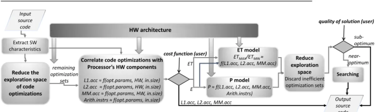
An abstract representation of the proposed methodology is illustrated in Fig. 1. First, all the characteristics of the loop kernels are extracted, i.e., array
references, array subscript equations, loop iterators and bounds, and iterator nesting level values.
Going from left to right in Fig. 1, in the first box (Subsection 3.1), we provide an efficient register blocking algorithm where loop unroll, scalar re-placement and register allocation are addressed together as one problem, and an efficient loop tiling algorithm where loop tiling and array copying are ad-dressed as one problem too. The transformations are carefully devised to fully exploiting the Register File (RF) size, cache size, cache line size and associa-tivity, data reuse and array data access patterns. One mathematical inequality is extracted for each memory, including RF. Each inequality provides all the efficient optimization sets. The implementations that do not obey to the ex-tracted inequalities are automatically discarded by our methodology pruning substantially the exploration space, while all the others are further processed. Although it is impractical to run all the different optimization sets / binaries in order to prove that our methodology does not discard efficient optimization sets, a theoretical explanation is given in Subsection 3.2.
Regarding the second box (Subsection 3.3) in Fig. 1, for all the remain-ing optimization sets, we approximate the number of L1 data cache (L1dc), L2 cache (L2c) and Main Memory (MM) accesses as well as the number of integer and Floating Point (FP) arithmetical instructions. This problem is theoretically formulated by exploiting the memory HW architecture details and the array memory access patterns of each loop kernel. In particular, one mathematical equation is generated for L1dc, L2c, MM, integer and FP arith-metical instructions, providing the corresponding number of memory accesses and arithmetical instructions. Therefore, the solution offering the minimum number of L1dc, L2c or MM accesses can be provided. It is important to note that the separate memories optimization gives a different optimization set / schedule for each memory and these schedules cannot coexist, as by refining one, degrading another, e.g., the schedule minimizing the number of L2c ac-cesses and the schedule minimizing the number of MM acac-cesses cannot coexist. Next, an Execution Time (ET) model extending C-AMAT [56] [51] and a Power consumption (P) model based on mcpat [30] simulator, are developed. These models correlateETM AX, ETM IN and P (and as a consequenceE, as E=ET×P), to the number of memory accesses and arithmetical instructions, which are derived by the second box in Fig. 1. Given that the maximum and minimum values of ET and E are known for each optimization set, the exploration space can be further reduced.
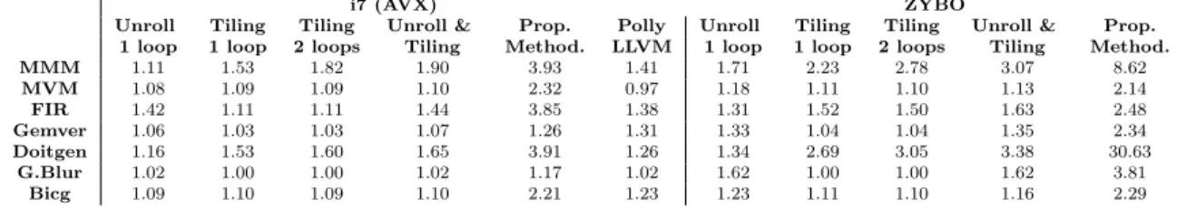
Finally, we can choose between a sub-optimum (good) solution fast or a near-optimum solution in a reasonable amount of time. In Subsection 4.3, we show that in the second case, we have to test from 46 up to 1800 binaries; we show that the exploration space is reduced from 17 up to 30 orders of magnitude and then it is practical to be searched.
HW architecture Reduce the exploration space of code optimizations Extract SW characteristics
Correlate code optimizations with P HW
L opt.params, HW, in.size)
L opt.params, HW, in.size)
MM opt.params, HW, in.size)
Arith.instrs opt.params, in.size)
ET model
ETMAX/ETMIN
f(L1.acc, L2.acc, MM.acc)
P model P L L MM Arith.instrs) remaining optimization sets
cost function (user)
quality of solution (user)
Searching
ET
L1.acc, L2.acc, MM.acc
sub-optimum near-optimum E Output source code Input source code Reduce exploration space Discard inefficient optimization sets
Fig. 1 Flow chart of the proposed methodology
3.1 Reduce the exploration space of code optimizations
In this Subsection we provide an efficient register blocking and loop tiling algorithm. The efficient application of loop tiling/blocking is not trivial and normally many different implementations are tested, since it a) depends on other transformations (e.g., array copying), b) depends on the target mem-ory architecture details, data reuse and data access patterns, c) increases the number of Load/Store (L/S) and arithmetical instructions. The application of loop tiling for the Register File (RF) is even more complex (register blocking). To our knowledge, no general (application independent) algorithm exists for register blocking; it is a mixture of loop tiling/loop unroll, scalar replacement and register allocation transformations. The efficient implementation of loop tiling/blocking is the key to the high performance and low energy SoftWare (SW), especially for data dominant applications [9].
The main steps of the proposed register blocking algorithm are the follow-ing:
1. Generate the subscript equations of all arrays
2. Generate the RF inequality (Eq. 1) that provides all the efficient optimiza-tion sets
3. Extract a transformation set from Eq. 1 4. Generate the code
Definition 1 Subscript equations which have more than one solution for at
least one constant value, are named type2 equations. All others, are named type1 equations.
For example, (A[2∗i+j]) gives the following type2 equation (2∗i+j=c1), while (A[i][j]) gives the following type1 equation (i=c21 andj =c22).
Each subscript equation defines the memory access pattern of the specific array reference. Obviously, in our methodology type1 and type2 arrays are treated with different policies as they access data in different ways. In this paper we give the formulas referring to type1 subscript equations only, as the corresponding formulas for type2 are more complicated (however, in Section 4 we have validated both).
The RF inequality gives the exact loops that loop unroll is applied to, their unroll factor values and the number of variables/registers allocated for each array. Each subscript equation contributes to the creation of Eq. 1, i.e., equationigivesAri and specifies its expression. The implementations that do
not obey to the extracted inequalities are discarded narrowing down the space substantially. The RF inequality is given by
n+Sc≤Ar1+Ar2+...+Arn+Sc≤F P (1)
whereF P is the number of the floating point (FP) registers,Scis the num-ber of FP scalar variables,Ari is the number of variables/registers allocated
for each array andnis the number of the array references. Without any loss of generality, in this paper we assume that the arrays contain FP data only and therefore we assume that the number of integer variables used is smaller than the number of integer registers. The upper bound of Eq. 1 derives from the fact that if more registers than the available are used, data are spilled to L1dc, increasing the number of L1 accesses. On the other hand, the lower bound value has been chosen as small as possible, because other constraints may be more critical; by using a larger lower bound value, register utilization is increased and therefore the number of L1 accesses is reduced; however, these optimization sets may conflict to those minimizing the number of MM or L2 accesses, which may be more critical.
The number of variables/registers allocated for each array is given by both (Ari=unrx×unry) and the three bullets below (the bullet points are given
in order to assign variables according to data reuse). The integer (unrx/unry)
are the unroll factor values of the iterators in the (x,y) dimension of the array’s subscript, e.g., the C[i][j] array in Fig. 2 gives (ArC = 1×4 = 4) (r1−r4
variables) as the (i, j) iterator unroll factor values are (1,4), respectively.
– For the type1 arrays which contain all the loop kernel iterators, only one register is needed (Ari= 1)
– For the innermost iterator always holds unr′ = 1 (the innermost iterator cannot be unrolled at this stage - however it can be unrolled in the output source code after)
– For the arrays i) containing more than one iterators and one of them is the innermost and ii) all iterators which do not exist in this array reference have unroll factor values equal to 1, then only one register is needed for this array (Ari = 1)
In the above three cases, a different element is accessed in each iteration (no data reuse is achieved) and thus wasting more than one register is not efficient, e.g., in Fig. 2, six registers are used, i.e., (ArC = 1×4, ArA= 1×1, ArB = 1).
Note that ArB = 1 instead ofArB = 4 because of the 3rd bullet above (a
different element of B is accessed in each k iteration and therefore it is not efficient to waste more than one register). Obviously, the scenario that not even one iterator is unrolled is not acceptable.
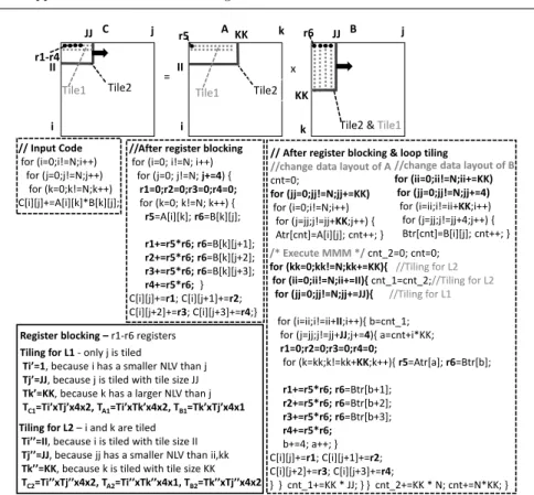
/* Execute MMM */ cnt_2=0; cnt=0; for (kk=0;kk!=N;kk+=KK){ //Tiling for L2
for (ii=0;ii!=N;ii+=II){ cnt_1=cnt_2;//Tiling for L2
for (jj=0;jj!=N;jj+=JJ){ //Tiling for L1
for (i=ii;i!=ii+II;i++){ b=cnt_1; for (j=jj;j!=jj+JJ;j+=4){ a=cnt+i*KK; r1=0;r2=0;r3=0;r4=0; for (k=kk;k!=kk+KK;k++){ r5=Atr[a]; r6=Btr[b]; r1+=r5*r6; r6=Btr[b+1]; r2+=r5*r6; r6=Btr[b+2]; r3+=r5*r6; r6=Btr[b+3]; r4+=r5*r6; b+=4; a++; } C[i][j]+=r1; C[i][j+1]+=r2; C[i][j+2]+=r3; C[i][j+3]+=r4; } } cnt_1+=KK * JJ; } } cnt_2+=KK * N; cnt+=N*KK; } //change data layout of B for (ii=0;ii!=N;ii+=KK)
for (jj=0;jj!=N;jj+=4) for (i=ii;i!=ii+KK;i++) for (j=jj;j!=jj+4;j++) { Btr[cnt]=B[i][j]; cnt++; } // After register blocking & loop tiling
//change data layout of A cnt=0;
for (jj=0;jj!=N;jj+=KK) for (i=0;i!=N;i++)
for (j=jj;j!=jj+KK;j++) { Atr[cnt]=A[i][j]; cnt++; }
Tiling for L2 i and k are tiled T II, because i is tiled with tile size II Tj JJ, because jj has a smaller NLV than ii,kk Tk KK, because k is tiled with tile size KK
TC2T T , TA2T T , TB2T T
Tiling for L1 - only j is tiled
Ti , because i has a smaller NLV than j Tj JJ, because j is tiled with tile size JJ Tk KK, because k has a larger NLV than j
TC1T T , TA1T T , TB1 T T
Register blocking r1-r6 registers // Input Code for (i=0;i!=N;i++) for (j=0;j!=N;j++) for (k=0;k!=N;k++) C[i][j]+=A[i][k]*B[k][j]; C A B r1-r4
Tile2 & Tile1 II II = x i i j k j k Tile1 Tile2 Tile1 Tile2
JJ r5 KK r6 JJ
KK
//After register blocking for (i=0; i!=N; i++)
for (j=0; j!=N; j+=4) { r1=0;r2=0;r3=0;r4=0; for (k=0; k!=N; k++) { r5=A[i][k]; r6=B[k][j]; r1+=r5*r6; r6=B[k][j+1]; r2+=r5*r6; r6=B[k][j+2]; r3+=r5*r6; r6=B[k][j+3]; r4+=r5*r6; } C[i][j]+=r1; C[i][j+1]+=r2; C[i][j+2]+=r3; C[i][j+3]+=r4;}
Fig. 2 An example, Matrix-Matrix Multiplication (MMM)
3≤unri×unrj+unri+unrj≤F P, unri6= 1&unrj6= 1
3≤unrj+ 2≤F P, unri= 1&unrj≻1
3≤unri+ 2≤F P, unrj= 1&unri≻1 (2)
The 3rd bullet generates 3 branches while the 2nd gives (unrk = 1). The
code shown in the second box of Fig. 2 refers to a second Eq. 2 branch solution, i.e., (unri= 1 and unrj= 4) and therefore 6 registers are used.
The main steps of the loop tiling algorithm are similar to those of the register blocking algorithm, but a cache inequality is generated instead (Eq. 3), one for each cache memory; each inequality contains the iterators that loop tiling is applied to, the tile sizes and the data array layouts (whether array copying has been applied or not). The implementations that do not obey to the extracted inequalities are automatically discarded by our methodology pruning the space.
The cache inequality is formulated as:
m≤ ⌈ T ile1
Li/assoc⌉+...+⌈ T ilen
Li/assoc⌉ ≤assoc (3)
whereT ileigives the tile size of the ith array in bytes,Liis the
cache,assoc= 8) andmdefines the lower bound of the tile sizes and it equals to the number of arrays in the loop kernel. The special case where the num-ber of the arrays is larger than the associativity value is not discussed in this paper (normally, (assoc≥8)). (⌈ T ile1
Li/assoc⌉) is an integer representing the
num-ber ofLicache lines with identical cache addresses used for the tile of array1.
Eq. 3 satisfies that the array tiles directed to the same cache subregions do not conflict with each other as the number of cache lines with identical addresses needed for the tiles is not larger than theassocvalue.
All the tile elements in Eq. 3 must contain consecutive MM locations. Oth-erwise, array copying is applied and an extra loop kernel is added for each array, likewise Atr and Btr arrays in Fig. 2; new arrays are created which replace the default ones, leading to extra cost in L/S and arithmetical instructions. There are some special cases where the arrays do not contain consecutive memory locations but their layouts can remain unchanged in order to avoid the cost of transforming the arrays, e.g., the tiles contain less or equal sub-rows than the number of cache ways and each sub-row is smaller than the size of one cache way; in this case, each sub-row is faced as a different tile.
T ilei which contains consecutive MM locations is given by Eq. 4:
T ilei= ( max
1≤j≤tiles(⌈
j×(T x×T y)
line ⌉ − ⌊
(j−1)×(T x×T y)
line ⌋))×line×type×s (4)
where the parenthesis gives the maximum size of the tile measured in cache lines (although the array’s tiles are of equal size, they occupy a different num-ber of cache lines), line is the cache line size in elements, type is the size of the array’s elements in bytes and the integer s defines how many tiles of each array should be allocated in the cache (s = 1 or s = 2). (Tx, Ty) are
the tile sizes of the iterators in the (x,y) dimension of the array’s subscript (for 1d arrays, T y = 1), tiles is the number of tiles for array i in total and (tiles = N/T y×M/T x) or (tiles =M/T x) whether for 2D/1D arrays, re-spectively ((N, M) are the iterators’ upper bound values).
Let us explain Eq. 4 through an example, consider an 1d array with (Ty=1,Tx=25) and line = 16 elements. First, the actual size of the tile is not 25 but 32, as the tiles are loaded in cache lines not elements. Second, the first tile occupies (⌈25
16⌉ − ⌊ 0
16⌋) = 2 cache lines, while the second tile occupies
(⌈5016⌉ − ⌊25
16⌋) = 3 cache lines.
Regardingsin Eq. 4, for the tiles that do not achieve data reuse and as a consequence a different tile is accessed in each iteration, we assign cache space twice the size of their tiles (s = 2). This way, not one but two consecutive tiles are allocated into the cache in order for the second accessed tile not to displace another array’s tile.
T′
i ((T x, T y) in Eq. 4) is given by one of the following three:
– the L1 tile size of the i iterator, if tiling for L1 is applied to the i iterator
– the unroll factor value of the i iterator, if tiling for L1 is not applied to the i iterator and i has a smaller nesting level value (NLV) than the iterator being tiled for L1
– the upper loop bound value of i iterator, if tiling for L1 is not applied to the i iterator and i has a larger NLV than the iterator being tiled for L1
Assuming an 8-way 32kbyte L1dc and MMM (Fig. 2), Eq. 3 gives (3 ≤ ⌈TC1 4096⌉+⌈ TA1 4096⌉+⌈ TB1
4096⌉ ≤8). The (TC1, TA1, TB1) values of the C-code shown
at the right of Fig. 2 are given in the bottom left box - to simplify the formulas, we assume that (KK modline= 0), (JJ modline= 0); also, floating point values are assumed, 4 bytes each (the NLV ofkiterator is 6 while the NLV of
kkis 1).
In the shared cache case, Li in Eq. 3 is the corresponding shared cache
partition size used and each core uses only its assigned shared cache space. We have implemented an automated C to C tool just for the seven studied algorithms, but a general tool can be implemented by using POET [45] tool. 3.2 Reduction of the exploration space in Subsection 3.1 - optimality
Although it is impractical to run all different optimization sets in order to prove that our methodology does not discard efficient schedules, a theoretical explanation is given.
The key idea of register blocking / loop tiling is to exploit the available registers / cache memory in order to reduce the number of data accesses to the next level memory in memory hierarchy. The optimization sets that don’t belong to Eq. 1, either use a larger number of registers than available or they don’t take into account data reuse (and therefore registers are wasted). The optimization sets that don’t belong to Eq. 3 either use larger tile sizes than the cache or the tiles cannot remain in the cache. Thus, the optimization sets that don’t belong to Eq. 1 and Eq. 3, refer to schedules where register blocking and loop tiling have not been applied in an efficient way, increasing the number of memory accesses in memory hierarchy. Although the optimization sets in Eq. 1 and Eq. 3 do not always provide near-optimum performance, as register blocking and loop tiling are not always performance efficient / desirable, Eq. 1 and Eq. 3 do provide all the efficient register blocking and loop tiling implementations, respectively. In other words, if the target metric is to minimize the number of memory accesses, then the optimum solution will be included in the corresponding inequality.
3.3 Approximate the number of memory accesses and arithmetical instructions
Formal methods are delivered approximating the number of L1dc, L2c and MM accesses as well integer and FP instructions to the optimization sets, HW architecture and input size. This problem is theoretically formulated by ex-ploiting the memory HW architecture details and the array memory access patterns of each loop kernel. More specifically, one mathematical equation is created for each memory and for each loop kernel providing the corresponding value. Loop tiling and loop unroll transformations and input size, are inserted directly to the aforementioned equations while array copying, scalar replace-ment and register allocation transformations and the HW architecture, are inserted indirectly (they have been used in order to create Eq.1-Eq.9).
We are capable of approximating the number of memory accesses through the whole memory hierarchy because no unexpected misses occur, as the tiles fit and remain in the cache. This is because only the proposed tiles reside in the cache, the tiles are written in consecutive MM locations, an empty cache line is always granted for each different modulo and we use cache space for two consecutive tiles and not one (when needed). Additionally,we refer to CPUs with an instruction cache; in this case, the program code typically fits in L1 instruction cache; thus, it is assumed that the shared cache or unified cache (if any) is dominated by data. Without loss of generality, this subsection assumes 2 levels of cache with equal line size and write-back write policy.
The equation approximating the number of L1dc accesses follows
L1.acc= i=arrays X i=1 ( j=M Y j=1 (upj−lowj) Tj × k=P Y k=1 Tk+of f seti) +var (5)
where arrays is the number of arrays, M is the number of the iterators that control the corresponding array andP is the number of the iterators that loop unroll has been applied to (iterators that exist in the subscript of the corresponding array only), e.g., regarding theC array in the code at the right of Fig. 2, the first product of Eq. 5 refers to all the iterators but k (array reference is outsidekloop) while the second product refers toj iterator only. (up, low, T) give the bound values of the corresponding iterator (normally, (up,low) define the algorithm’s input size);T refers to both tile size and unroll factor value according to the corresponding iterator.
of f set gives the number of L1 data accesses of the new loop kernel added in the case the data array layout is transformed (array copying transformation is applied). Offset is either (of f seti = 2×ArraySizei) or (of f seti = 0)
depending on whether the data layout of the array is changed or not; in the case that the layout is changed, the array has to be loaded and then written again to memory, thus it is (of f seti = 2×ArraySizei). (var) gives the number
of L1 accesses due to the scalar variables; given that we never use more registers than available, no RF spills occur and thus (var≈0).
Eq. 5 for the C-code at the right of Fig. 2 gives (2× N3 KK,
N3 4 , N
3) L1
accesses for (C, A, B) arrays, respectively (C is both loaded and stored), and in overall (L1.acc= 2×KKN3 +N43 +N3+ 4×N2).
As far as the number of L2c and MM accesses are concerned, they are measured in cache lines not in elements. In this paper we give the formulas referring to type1 subscript equations only, as the corresponding formulas for type2 are more complex; however, in Section 4 we have validated both.
The number of L2c accesses is approximated by Eq. 6; at this step, only the new/extra iterators (introduced by loop tiling) are processed and not the initial iterators exist in the input code.
L2Acc.=Pii==1arrays(times.accessedi×L2c.linesi+of f seti) +code (6)
wherearraysis the number of the arrays,times.accessedigives how many
times arrayi is accessed from L2c and is given by Eq. 8 andL2c.lines is the number of L2c lines accessed for every iand is given by Eq. 7 (although the
array’s tiles are of the same size, they occupy a different number of cache lines).
of f setgives the number of L2c lines accessed because of the new loop kernel added when array copying is applied (the data array layout is transformed) andcoderefers to code/instruction accesses and always (Arrays acc.≫code) as a) the code size of loop kernels is small and fits in L1 instruction cache, b) we are dealing with data dominant algorithms.
L2c.lines= N T y×T y× j=M/T x X j=1 (⌈j×T x line ⌉ − ⌊ (j−1)×T x
line ⌋),row-wise data array layout
j=tiles X j=1 (⌈j×(T x×T y) line ⌉ − ⌊ (j−1)×(T x×T y) line ⌋),tile-wise (7) where (T x, T y) are the tile sizes of the iterators in the (x,y) dimension of the array’s subscript, respectively, (N, M) are the corresponding iterators’ upper bounds (for 1D arraysT y= 1), lineis the cache line size in elements,
tilesis the number of tiles for arrayiin total and (tiles=N/T y×M/T x) or (tiles=M/T x) whether for 2D/1D arrays, respectively.
Let us give an example for the first branch of Eq. 7, consider a 2D floating point array and a tile of size (10×10) traversing the array in the x-axis. Also consider that (line= 16) array elements. The first tile occupies 10×(⌈1016⌉ − ⌊160⌋) = 10 cache lines while the second tile occupies 10×(⌈2016⌉ − ⌊1016⌋) = 20 cache lines. Although the array’s tiles are of equal size, they occupy a different number of cache lines. If the array in the previous example is written tile-wise in MM, then the first tile lies between (0,100), the second between (100,200) etc. times.accessed=Qjj==1N (upj−lowj) Tj × Qk=M k=1 (upk−lowk) Tk (8)
where N is the number of new/extra iterators (generated by loop tiling) that a) do not exist in the corresponding array’s subscript and b) exist above of the iterators of the corresponding array. M is the number of new/extra iterators that a) do not exist in the array and b) exist between of the iterators of the array, e.g., regarding (C, A, B) arrays in Fig. 2, the iterators referring to the first and second product of Eq. 8 are (kk, none), (jj, none), (none, ii), respectively, giving (KKN ), (JJN) and (IIN), respectively.
The number of MM accesses is given by an equation identical to Eq. 6. However, regardingtimes.accessedvalue in Eq. 8, we refer only to the iterators created by applying tiling to the last level cache, e.g., regarding (C, A, B) arrays of MMM (Fig. 2), the iterators referring to the first and second product of Eq. 8 are (kk, none), (none, none), (none, ii), respectively, giving (tC =
N
KK), (tA= 1) and (tB = N
II), respectively.
In the case that more than one threads run in parallel under a shared cache, the overall number of accesses is extracted by accumulating all the different loop kernel equations. No more than p threads run in parallel, one to each core, where pis the number of the cores. Different threads access only their assigned shared cache space and thus different thread tiles do not conflict with each other [21].
The number of integer or FP instructions is approximated by: Arith. instrs= i=iteratorsX i=1 ( j=i Y j=1 upj−lowj Tj ×cj) +of f set (9)
where iteratorsis the total number of iterators and (up, low, T) are their corresponding bound values, as in previous equations. cj is the number of
integer or FP assembly instructions measured insidejloop (assembly instruc-tions occur between the open and close loop bracket).of f set is the number of arithmetical instructions of the extra loop kernels added (if array copying is applied, i.e., the array layouts change).
(Pii==1iterators(Qjj==1i upj−lowj
Tj ) gives the number of loop iterations in total
while cj gives the number of assembly instructions in loop j. Note that j
iterator varies from (j = 1 - it corresponds to the outermost iterator) to (j=iterators- it corresponds to the innermost iterator), e.g., in Fig. 2, Eq. 9 gives ((N/KK)×c1 + (N2/(KK×II))×c2 + (N3/(KK×II×JJ))×c3 +
(N3/(KK ×JJ))×c4 + (N3/(KK ×4))×c5 + (N3/4)×c6); as it can be
observed, the number of arithmetical instructions is strongly affected by a) the number of the loops being tiled (more terms are introduced), b) tile size / unroll factor values of the innermost iterators (here, the unroll factor value ofj, i.e., 4, affects the number of instructions at the most).
Given that thecvalues depend on the target compiler, they cannot be ap-proximated. Thus, we measure thecvalues for one transformation set and pre-dict thecvalues of the others (where possible), e.g., in Fig. 2, thecvalues (as-sembly instructions) almost remain unchanged by changing the (KK, II, JJ) values (apart from their maximum and minimum ones because in this case, the number of the loops changes), but not by changing the (j) unroll factor value or the number of the loops being tiled, because the loop body changes and thus more/less assembly instructions are inserted.
We take advantage of the fact that the cvalues almost remain unchanged for different tile sizes, suffice the array layouts remain unchanged and the tile sizes do not take their maximum/minimum values. In Subsection 4.1, we show that we can approximate the number of arithmetical instructions with very good accuracy, even using ’O2’ optimization level. The c values for different unroll factor values and data layouts are significantly changed and cannot be predicted.
3.4 Execution Time (ET) model
Modern memory systems support concurrent data accesses at each layer of the memory hierarchy and therefore the ET value cannot be given by the well known AMAT model, but by its extension, i.e., C-AMAT [56] [51], where the notions of hit/miss concurrency and pure miss, are introduced. A pure miss, is a cache miss which contains at least one pure miss cycle, which is a cycle that does not overlap with a hit cycle. The intuition behind pure misses is based on the fact that not all cache misses will cause processor stall, but rather only pure misses. So, according to C-AMAT, the access time of a single memory is given by (H/CH+(pM R×pAM P)/CM), whereH andCHare the hit latency
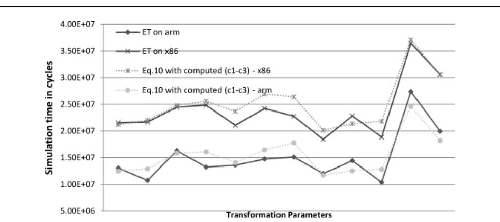
5.00E+06 1.00E+07 1.50E+07 2.00E+07 2.50E+07 3.00E+07 3.50E+07 4.00E+07 S im u la ti o n t im e i n c y cl e s Transformation Parameters ET on arm ET on x86
Eq.10 with computed (c1-c3) - x86 Eq.10 with computed (c1-c3) - arm
Fig. 3 Simulated and approximated ET values for Matrix-Matrix Multiplication (MMM) algorithm
and hit concurrency,pM RandpAM P are the pure miss rate and pure average miss penalty andCM is the average pure miss concurrency.
The parameter CH represents hit concurrency, which results from
multi-port, multibanked and pipelined cache structures, while the parameter CM
represents miss concurrency, which results from nonblocking cache structures and data prefetching; these parameters can also represent both hit concur-rency and miss concurconcur-rency that result from processor ILP design techniques, such as out-of-order execution and multiple issue pipelining. Furthermore, 1≤ CH≤CHmaxwhere (Cmax= #cacheports×#cache.related.pipeline.stages)
and 1≤ CM ≤CM max where CM max is determined by the number of miss
status holding register (MSHR) entries.
C-AMAT cannot be used by our method in its current form as the number of pure misses is unknown; thus we adopt C-AMAT’s idea and construct the following formula to approximate the ET for data dominant loop kernels:
ET
≈
T
data≈
L1.acc×L1.latc1
+
L2.acc×L2.lat
c2
+
M M.acc×M M.max.latc3 (10)where (L1.lat, L2.lat, M M.max.lat) are the L1,L2 and maximum MM la-tency values (L2.lat and M M.latrefer to the time needed for a whole cache line to be loaded),c1 =CH and (c2-c3) give both hit and miss concurrency.
(c1-c3) values depend on both HW and SW and (ci ≥ 1). The L1 and L2
latency values are constants while MM’s latency (M M.lat) is not (the reason follows).
MM can be considered as a 2D array. M M.lat is mainly affected by a) the time needed to find and activate the desired row (aka MM page), b) find the desired column, c) transfer the desired word; keep in mind that if the next desired word is a) the following, it is transferred at minimum cost, b) in the same page, it is transfered at low cost, c) in another row, in great cost as another row has to be decoded and activated. Although our methodology optimizes MM accesses and thereforeM M.latvalue is kept low (on average), we insert its upper bound in Eq. 10, i.e., M M.max.lat, and its lower values are handled through c3.
An analysis on which parameters affect (c1-c3) follows. The (c1-c3) vary de-pending on both HW and SW characteristics and therefore different processors and different optimization sets give different (c1-c3) values. As it has briefly explained above, thec3 value refers to both MM latency and concurrency and thereforec3 depends on the data access patterns and on how arrays have been stored into MM; accessing consecutive data and data from the same memory bank gives a higher c3 value; moreover, by accessing consecutive data, the HW prefetchers are enabled and therefore c3 is further increased. Regarding c2, its value is increased when the tiles that reside in L2 are accessed multiple times (reused) and when the L2 cache lines are utilized (spatial locality), as the probability of fetching data from L2 when an L2 miss has been occurred is increased. Furthermore, accessing consecutive cache lines enables the L1 HW prefetchers (if any). Likewise, c1 depends on data reuse in L1 but also on the ratio between the L/S and array arithmetic (in this paper FP) instructions in the loop kernel (L/S.ratio); high ratio values refer to low register usage and Instruction Per Cycle (IPC) values and as a consequence to low c1 values. The
L/S.ratiois affected by the register blocking algorithm applied in Subsection 3.1. It is important to note that all the optimization sets generated by Subsec-tion 3.1 use consecutive MM locaSubsec-tions, achieve data reuse and lowL/S.ratio
values.
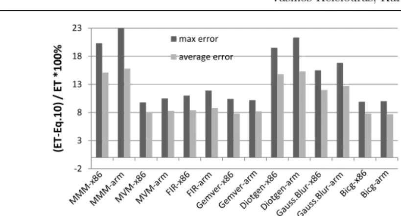
So, the key idea is that although (c1-c3) vary depending on both HW and SW characteristics, their variation is low, as all the remaining optimization sets used in Eq. 10: a) refer to the same CPU and MM, and loop kernel and b) have similar data access behavior (consecutive data accesses, data reuse etc). Given that first, ET ≈ f(L1.acc, L2.acc, M M.acc) and second, the number of memory accesses have been approximated for each optimization set, the (c1-c3) values can be computed by measuring the ET value of three or more optimization sets and solving the system of equations. The (c1-c3) values are computed by using three or more samples (runs); as samples, we can chose the ones achieving a very low Eq. 10 value, as they are more than likely to belong to the final exploration space and thus tested/run anyway. We have plotted Eq. 10 together with the simulated ET of different versions of seven loop kernels on two different processors and the Eq. 10 follows the trend in all cases; the algorithm giving the highest variation is MMM and is shown in Fig. 3. In Subsection 4.2, we show that the percent error in Eq. 10 is about 11% on average and 23% at maximum. It is important to note that part of the variation is because of the error occurred in computing the number of data accesses (about 2%-3%).
To conclude, the ET values of the Subsection 3.1 binaries can be bounded and generate ETM AX/ETM IN values, as each point in Fig. 3 varies only
be-tween±23% (at maximum) and therefore the exploration space can be further reduced (the scope of this paper is not to find the exact threshold value but to showcase the methodology). Alternatively, we can select a ’good’ optimiza-tion set fast, without searching, by using Eq. 10 with median c1-c3 values, as the aforementioned equation is a good metric to chose an efficient schedule qualitatively.
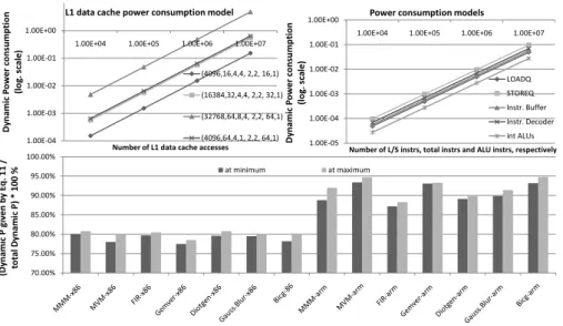
Last, in this paper we refer to algorithms whose ET mainly depends on the number of data accesses, but Eq.10 can be extended to algorithms whose ET value is affected by the number of arithmetical instructions too (approximated by Eq.9). 70.00% 75.00% 80.00% 85.00% 90.00% 95.00% 100.00% (D y n a m ic P g iv e n b y E q . 1 1 / to ta l D y n a m ic P ) * 1 0 0 % at minimum at maximum 1.00E-04 1.00E-03 1.00E-02 1.00E-01 1.00E+00
1.00E+04 1.00E+05 1.00E+06 1.00E+07
D y n a m ic P o w e r co n su m p ti o n (l o g . sc a le )
Number of L1 data cache accesses
L1 data cache power consumption model
(4096,16,4,4, 2,2, 16,1) (16384,32,4,4, 2,2, 32,1) (32768,64,8,4, 2,2, 64,1) (4096,64,4,1, 2,2, 64,1) 1.00E-05 1.00E-04 1.00E-03 1.00E-02 1.00E-01 1.00E+00
1.00E+04 1.00E+05 1.00E+06 1.00E+07
D y n a m ic P o w e r co n su m p ti o n (l o g . sc a le )
Number of L/S instrs, total instrs and ALU instrs, respectively
Power consumption models
LOADQ STOREQ Instr. Buffer Instr. Decoder int ALUs
Fig. 4 Power consumption models
3.5 Power consumption (P) model
It is clear that the aforementioned transformations affect P in all the CPU components and MM and thus a different P model is generated for each dif-ferent CPU and MM. First, we made a detailed analysis on which parameters affect P on each CPU component. L1dc and L2c P values are linear to the number of L1dc/L2c accesses (approximated by Eq. 5 and Eq. 6) while af-fected by the HW architecture set (cache size,cache line size, associativity, number of banks, throughput, latency,output width, cache policy - Fig. 4). Similarly, the DDR P values are linear to the number of MM accesses, while affected by the number of memory controllers, number of channels, number of ranks, block size, transfer rate, databus width etc. LoadQ/StoreQ P values are linear to the number of L/S instructions (approximated by Eq. 5). The ALU, instruction buffer and instruction decoder P values are linear to the number of ALU instructions and total number of instructions (Eq. 9+Eq. 5), respectively (Fig. 4). Second, an off-line training phase is applied for the target CPU and MM, in order to generate the corresponding P equations; the custom HW architecture is given as input to the mcpat [30] simulator and a number of simulations takes place for different values of L1dc,L2c,MM accesses and int, FP instructions. Although this work can be extended to take into account
more CPU components, in this paper, we approximate P by using Eq. 11; thus, we do not take into account P on the renaming unit, instruction cache, RF, TLBs, branch predictor and instruction scheduler.
P =PL1(f(L1.acc)) +PL2(f(L2.acc)) +PDDR(f(DDR.acc))+
PL/S Queue(f(L/S.instrs)) +PALU(f(ALU.instrs))+
Pinstr.buf f er(f(instrs)) +Pinstr.decoder(f(instrs))
(11) The coefficients of Eq. 11 are derived by the custom CPU and MM charac-teristics (off-line training phase). The independent variables of Eq. 11 are the memory access and instruction values given in Subsection 3.3.
Regarding Energy consumption (E), it is the product of Eq. 10 and Eq. 11; thus, if the target metric is E, we can either bound the new equation and apply searching or select a ’good’ schedule qualitatively as in the previous subsection.
Algorithm 1: Proposed Methodology
Step 1.extract SW characteristics
Step 2.apply proposed Register blocking algorithm
for(all different optimization sets (RF sets))do
Step 3.apply loop tiling alg. to L1
for(all different optimization sets (L1 sets))do
Step 4.apply loop tiling alg. to L2
for(all different optimization sets (L2 sets))do
Step 5a.generate the memory access equations - Eq. 5-Eq. 8 (all memories)
Step 5b.compute the num of accesses in memory hierarchy
Step 6.arithmetical instructions
if(the num of arith. instrs cannot be predicted for the current set)then
generate output C code (from C to C) for the current set generate assembly code - cross compile
measure the num of FP and integer assembly instrs (get the c values of Eq. 9)
else
predict the num of arith. instrs (Eq. 9)
end if
Step 7.compute the ET,P,E values for the current set
Step 8.store only the best set(s) depending on the cost function (ET,E,L1,L2,MM)
end for
change the nesting level values of the iterators generated in step4
end for
change the nesting level values of the iterators generated in step3
end for
3.6 Proposed framework - Putting it all together
The proposed methodology is given in Algorithm 1. All the steps have been explained in the previous subsections. All different combinations of loop inter-change are generated as it affects the proposed equations.
In the case that the target metric is not the ET or E but the minimum number of Li memory accesses and therefore the minimum number of L1dc,
L2c or MM accesses is requested, then Algorithm 1 is changed accordingly, i.e., steps (1,2,5,8), (1,3,5,8) or (1,4,5,8) are executed only, respectively. It is important to note that in this case the number of different optimization sets that have to be further processed by Subsection 3.3 is smaller, i.e., the lower bound values of Eq. 1 and Eq. 3 are no longer needed to be that small. For example, by using a larger lower bound value in Eq. 1, register utilization is increased and therefore the number of L1 accesses is reduced; however, as we have already explained in Subsection 3.1, these optimization sets may conflict to those minimizing the number of MM or L2c accesses, which may be more critical. Thus, if the binary achieving the minimum number of L1 accesses is requested, there is no need to use such a small Eq. 1 lower bound value. The same holds for L2c and MM too.
0 0.5 1 1.5 2 2.5 3 3.5 4 M a x im u m E rr o r (%) -n u m b e r o f m e m o ry a cc e ss e s
L1-Reads L1-Writes L2-Reads L2-Writes MM-Reads MM-Writes
0 5 10 15 20 25 30 35 40 E rr o r (%) -n u m b e r o f in te g e r in st ru ct io n s MMM MVM FIR Gemver Diotgen Gaussian Blur Bicg
Fig. 5 Validation of Eq.5-Eq.9
4 Experimental Results
The proposed methodology has been evaluated in terms of memory accesses, arithmetical instructions, ET, P, E and exploration space. The experimen-tal results are obtained by using a) gem5 [8] and McPAT [30] simulators, simulating both a generic x86 and an ARMv8-A CPU b) the quad-core Intel i7 6700 CPU (CentoS-7 OS) by using both normal C-code and hand written
-2 3 8 13 18 23 (E T -E q .1 0 ) / E T *1 0 0 % max error average error
Fig. 6 Validation of the ET model in Subsection 3.4 - range between measured ET and Eq.10
code with AVX extensions, c) the embedded ARM Cortex-A9 processor on a Zybo Zynq-7000 FPGA platform using petalinux OS. The gem5 cache subsys-tem consists of a 4K, 64 byte block, 8-way, dual-ported, 2 cycle L1 data and instruction caches and a 16-way, 32KB L2, 20-cycle L2 cache. The gem5 simu-lation results are forwarded as input to McPAT; McPAT provides dynamic and leakage power values of both processor and main memory in detail. The energy consumption is computed by (Etotal= (Pdynamic+Pleakage)∗Exec.time).
The bench-suite used in this study consists of seven well-known data domi-nant static kernels taken from PolyBench/C benchmark suite version 4.1 [39]. These are: Matrix-Matrix Multiplication (MMM), Matrix-Vector Multiplica-tion (MVM), Gaussian Blur (3×3 filter), Finite Impulse Response filter (FIR), a kernel containing mixed vector multiplication and matrix addition (Gemver - first loop kernel only), a multiresolution analysis kernel (Doitgen) and BiCG sub Kernel (Bicg). The source code of the bench-suite used, is given in Fig. 7. The kernels are compiled using gcc 4.9.4 and arm-linux-gnueabi-gcc 4.9.2 com-pilers, for x86 and arm, respectively. The proposed method is compared to gcc ’O3’ option as well as to hand written optimized code and Polly [16]. The proposed methodology output C-codes are compiled with ’O2’ optimization level in order to the compiler be less aggressive.
4.1 Validation of Eq.5-Eq.9
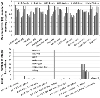
First, a validation on the number of L1, L2 and MM accesses is given and in particular Eq.5-Eq.8, on gem5 simulator; the number of memory accesses has been measured for different optimization sets and the maximum percent error (error% = |experimentaltheoretical−theoretical|×100) values are shown (Fig. 5). The proposed equations give from 2.2% up to 3.6% less accesses.
Second, a validation on the number of arithmetical instructions is given (Eq. 9) for both normal C-code and hand written code with AVX instruc-tions and 2 different compilers with both ’O1’ and ’O2’ opinstruc-tions (Fig. 5). The
//MMM for (i=0;i!=N;i++) for (j=0;j!=N;j++) for (k=0;k!=N;k++) C[i][j]+=A[i][k]*B[k][j]; //MVM for (i=0;i<M;i++) for (j=0;j<M;j++) Y[i]+=A[i][j]*X[j]; //FIR for( i = 0; i < N ; i++ ) for( j = 0; j < M; j++ )
out[i] += in[ i + j ] * kernel[ j ];
//GEMVER for (i = 0; i < N; i++)
for (j = 0; j < N; j++)
A[i][j] += u1[i] * v1[j] + u2[i] * v2[j]; //Gaussian Blur
for (row = 1; row < N-1; row++) { for (col = 1; col < M-1; col++) {
tmp=0;
for (row2=-1; row2<=1; row2++) { for (col2=-1; col2<=1; col2++) {
tmp += (image[row+row2][col+col2] * mask[1+row2][1+col2]); } } image2[row][col]=tmp/const; } } //Diotgen for (r = 0; r < N; r++) for (q = 0; q < N; q++) for (p = 0; p < N; p++) for (s = 0; s < N2; s++)
sum[r][q][p] = sum[r][q][p] + A[r][q][s] * C[s][p];
//MMM
//B array has been transposed to column-wise
for (i=0;i!=N;i++) for (j=0;j!=N;j++){ ymm0= _mm256_setzero_ps(); for (k=0;k!=N;k+=8){ ymm1=_mm256_load_ps( &A[i][k]); ymm2=_mm256_load_ps( &B2[j][k]); ymm0+=_mm256_mul_ps(ymm1,ymm2); }
ymm2 = _mm256_permute2f128_ps(ymm0 , ymm0 , 1); ymm0 = _mm256_add_ps(ymm0, ymm2);
ymm0 = _mm256_hadd_ps(ymm0, ymm0); ymm0 = _mm256_hadd_ps(ymm0, ymm0); xmm1=_mm256_extractf128_ps(ymm0,0) _mm_store_ss((float *) &C[i][j], xmm1); } //MVM for (i=0;i!=M;i++){ num1= _mm256_setzero_ps(); for (j=0;j<M;j+=8){ num5=_mm256_load_ps(X + j ); num0=_mm256_load_ps(&A[i][j]); num1+=_mm256_mul_ps(num0,num5); }
ymm2 = _mm256_permute2f128_ps(num1 ,num1,1); num1 = _mm256_add_ps(num1, ymm2);
num1 = _mm256_hadd_ps(num1, num1); num1 = _mm256_hadd_ps(num1, num1); xmm2=_mm256_extractf128_ps(num1,0); _mm_store_ss((float *) Y+i, xmm2); } //FIR for( i = 0; i != N; i++ ){ num1= _mm256_setzero_ps(); for( j = 0; j != M; j+=8 ){ num5=_mm256_load_ps(kernel + j ); num0=_mm256_loadu_ps(in +i+j); num1+=_mm256_mul_ps(num0,num5); }
ymm2 = _mm256_permute2f128_ps(num1 ,num1,1); num1 = _mm256_add_ps(num1, ymm2);
num1 = _mm256_hadd_ps(num1, num1); num1 = _mm256_hadd_ps(num1, num1); xmm2=_mm256_extractf128_ps(num1,0); _mm_store_ss((float *) out+i, xmm2); }
//Diotgen
//Ctr array has been transposed to column-wise
for (r = 0; r < N; r++) for (q = 0; q < N; q++) for (p = 0; p < N; p++) { num3= _mm256_setzero_ps(); for (s = 0; s < N2; s+=8){ num1=_mm256_load_ps(&A[r][q][s]); num2=_mm256_load_ps(&Ctr[s][p]); num3+=_mm256_mul_ps(num1,num2); }
ymm2 = _mm256_permute2f128_ps(num3 , num3 , 1); num3 = _mm256_add_ps(num3, ymm2);
num3 = _mm256_hadd_ps(num3, num3); num3 = _mm256_hadd_ps(num3, num3); xmm2=_mm256_extractf128_ps(num3,0); _mm_store_ss((float *)&sum[r][q][p], xmm2); } //GEMVER for (i=0;i!=N;i++){ xmm1=_mm_load_ps1(u1 + i); xmm2=_mm_load_ps1(u2 + i); num3=_mm256_broadcast_ps(&xmm1); num4=_mm256_broadcast_ps(&xmm2); for (j=0;j<N;j+=8){ num1=_mm256_load_ps(v1 + j); num2=_mm256_load_ps(v2 + j); num5=_mm256_mul_ps(num1,num3); num5+=_mm256_mul_ps(num2,num4); num6=_mm256_load_ps(&A[i][j]); num6+=num5;
_mm256_store_ps((float *) &A[i][j], num6); } } //Gaussian Blur for (i = 1; i < N-1; i++) { for (j = 1; j < M-1; j++) { r0 = _mm_loadu_si128((__m128i *) &image[i-1][j-1]); r0 = _mm_madd_epi16(r0,const0); r1 = _mm_loadu_si128((__m128i *) &image[i][j-1]); r1 = _mm_madd_epi16(r1,const1); r2 = _mm_loadu_si128((__m128i *) &image[i+1][j-1]); r2 = _mm_madd_epi16(r2,const2); r0 = _mm_add_epi32(r0,r1); r2 = _mm_add_epi32(r2,r0); r11 = _mm_cvtepi32_ps(r2); r11 = _mm_hadd_ps(r11,r11); r11 = _mm_div_ps(r11,const3); _mm_store_ss((float *) &image2[i][j], r11); } }
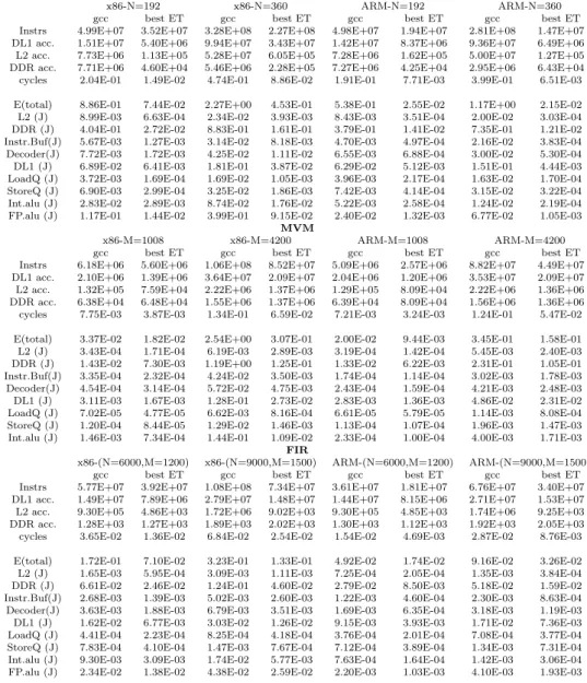
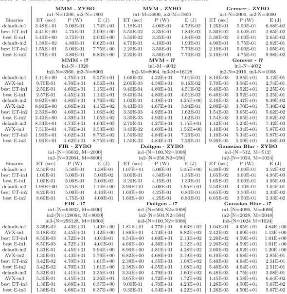
Table 1 Evaluation over gcc using gem5 and mcpat (MMM, MVM and FIR)
MMM
x86-N=192 x86-N=360 ARM-N=192 ARM-N=360 gcc best ET gcc best ET gcc best ET gcc best ET Instrs 4.99E+07 3.52E+07 3.28E+08 2.27E+08 4.98E+07 1.94E+07 2.81E+08 1.47E+07 DL1 acc. 1.51E+07 5.40E+06 9.94E+07 3.43E+07 1.42E+07 8.37E+06 9.36E+07 6.49E+06 L2 acc. 7.73E+06 1.13E+05 5.28E+07 6.05E+05 7.28E+06 1.62E+05 5.00E+07 1.27E+05 DDR acc. 7.71E+06 4.60E+04 5.46E+06 2.28E+05 7.27E+06 4.25E+04 2.95E+06 6.43E+04 cycles 2.04E-01 1.49E-02 4.74E-01 8.86E-02 1.91E-01 7.71E-03 3.99E-01 6.51E-03 E(total) 8.86E-01 7.44E-02 2.27E+00 4.53E-01 5.38E-01 2.55E-02 1.17E+00 2.15E-02 L2 (J) 8.99E-03 6.63E-04 2.34E-02 3.93E-03 8.43E-03 3.51E-04 2.00E-02 3.03E-04 DDR (J) 4.04E-01 2.72E-02 8.83E-01 1.61E-01 3.79E-01 1.41E-02 7.35E-01 1.21E-02 Instr.Buf(J) 5.67E-03 1.27E-03 3.14E-02 8.18E-03 4.70E-03 4.97E-04 2.16E-02 3.83E-04 Decoder(J) 7.72E-03 1.72E-03 4.25E-02 1.11E-02 6.55E-03 6.88E-04 3.00E-02 5.30E-04 DL1 (J) 6.89E-02 6.41E-03 1.81E-01 3.87E-02 6.29E-02 5.12E-03 1.51E-01 4.44E-03 LoadQ (J) 3.72E-03 1.69E-04 1.69E-02 1.05E-03 3.96E-03 2.17E-04 1.63E-02 1.70E-04 StoreQ (J) 6.90E-03 2.99E-04 3.25E-02 1.86E-03 7.42E-03 4.14E-04 3.15E-02 3.22E-04 Int.alu (J) 2.83E-02 2.89E-03 8.74E-02 1.76E-02 5.22E-03 2.58E-04 1.24E-02 2.19E-04 FP.alu (J) 1.17E-01 1.44E-02 3.99E-01 9.15E-02 2.40E-02 1.32E-03 6.77E-02 1.05E-03
MVM
x86-M=1008 x86-M=4200 ARM-M=1008 ARM-M=4200 gcc best ET gcc best ET gcc best ET gcc best ET Instrs 6.18E+06 5.60E+06 1.06E+08 8.52E+07 5.09E+06 2.57E+06 8.82E+07 4.49E+07 DL1 acc. 2.10E+06 1.39E+06 3.64E+07 2.09E+07 2.04E+06 1.20E+06 3.53E+07 2.09E+07 L2 acc. 1.32E+05 7.59E+04 2.22E+06 1.37E+06 1.29E+05 8.09E+04 2.22E+06 1.36E+06 DDR acc. 6.38E+04 6.48E+04 1.55E+06 1.37E+06 6.39E+04 8.09E+04 1.56E+06 1.36E+06 cycles 7.75E-03 3.87E-03 1.34E-01 6.59E-02 7.21E-03 3.24E-03 1.24E-01 5.47E-02 E(total) 3.37E-02 1.82E-02 2.54E+00 3.07E-01 2.00E-02 9.44E-03 3.45E-01 1.58E-01 L2 (J) 3.43E-04 1.71E-04 6.19E-03 2.89E-03 3.19E-04 1.42E-04 5.45E-03 2.40E-03 DDR (J) 1.43E-02 7.30E-03 1.19E+00 1.25E-01 1.33E-02 6.22E-03 2.31E-01 1.05E-01 Instr.Buf(J) 3.35E-04 2.32E-04 4.24E-02 3.50E-03 1.74E-04 1.14E-04 3.02E-03 1.78E-03 Decoder(J) 4.54E-04 3.14E-04 5.72E-02 4.75E-03 2.43E-04 1.59E-04 4.21E-03 2.48E-03 DL1 (J) 3.11E-03 1.67E-03 1.28E-01 2.73E-02 2.83E-03 1.36E-03 4.86E-02 2.31E-02 LoadQ (J) 7.02E-05 4.77E-05 6.62E-03 8.16E-04 6.61E-05 5.79E-05 1.14E-03 8.08E-04 StoreQ (J) 1.20E-04 8.44E-05 1.29E-02 1.46E-03 1.13E-04 1.07E-04 1.96E-03 1.47E-03 Int.alu (J) 1.46E-03 7.34E-04 1.44E-01 1.09E-02 2.33E-04 1.00E-04 4.00E-03 1.71E-03
FIR
x86-(N=6000,M=1200) x86-(N=9000,M=1500) ARM-(N=6000,M=1200) ARM-(N=9000,M=1500) gcc best ET gcc best ET gcc best ET gcc best ET Instrs 5.77E+07 3.92E+07 1.08E+08 7.34E+07 3.61E+07 1.81E+07 6.76E+07 3.40E+07 DL1 acc. 1.49E+07 7.89E+06 2.79E+07 1.48E+07 1.44E+07 8.15E+06 2.71E+07 1.53E+07 L2 acc. 9.30E+05 4.86E+03 1.72E+06 9.02E+03 9.30E+05 4.85E+03 1.74E+06 9.25E+03 DDR acc. 1.28E+03 1.27E+03 1.89E+03 2.02E+03 1.30E+03 1.12E+03 1.92E+03 2.05E+03 cycles 3.65E-02 1.36E-02 6.84E-02 2.54E-02 1.54E-02 4.69E-03 2.87E-02 8.76E-03 E(total) 1.72E-01 7.10E-02 3.23E-01 1.33E-01 4.92E-02 1.74E-02 9.16E-02 3.26E-02 L2 (J) 1.65E-03 5.95E-04 3.09E-03 1.11E-03 7.25E-04 2.05E-04 1.35E-03 3.84E-04 DDR (J) 6.61E-02 2.46E-02 1.24E-01 4.60E-02 2.79E-02 8.50E-03 5.18E-02 1.59E-02 Instr.Buf(J) 2.68E-03 1.39E-03 5.02E-03 2.60E-03 1.22E-03 4.60E-04 2.30E-03 8.63E-04 Decoder(J) 3.63E-03 1.88E-03 6.79E-03 3.51E-03 1.69E-03 6.35E-04 3.18E-03 1.19E-03 DL1 (J) 1.62E-02 6.77E-03 3.03E-02 1.26E-02 9.15E-03 3.93E-03 1.71E-02 7.36E-03 LoadQ (J) 4.41E-04 2.23E-04 8.25E-04 4.18E-04 3.76E-04 2.01E-04 7.08E-04 3.77E-04 StoreQ (J) 7.83E-04 4.10E-04 1.47E-03 7.67E-04 7.12E-04 3.89E-04 1.34E-03 7.31E-04 Int.alu (J) 9.30E-03 3.09E-03 1.74E-02 5.77E-03 7.63E-04 1.64E-04 1.42E-03 3.06E-04 FP.alu (J) 2.34E-02 1.38E-02 4.38E-02 2.59E-02 2.20E-03 1.03E-03 4.10E-03 1.93E-03
number of integer instructions is measured for one transformation set and then predicted for the others; we take advantage of the fact that the c val-ues almost remain unchanged for different tile sizes. The insertion of an extra assembly instruction in the innermost/outermost loop body, leads to a sig-nificant/meaningless error value in Eq. 9, respectively. ’O1’ option gives a meaningless error in all cases. Regarding ’O2’ option, there is an extremely small number of specific tile sizes that affect the innermost assembly loop
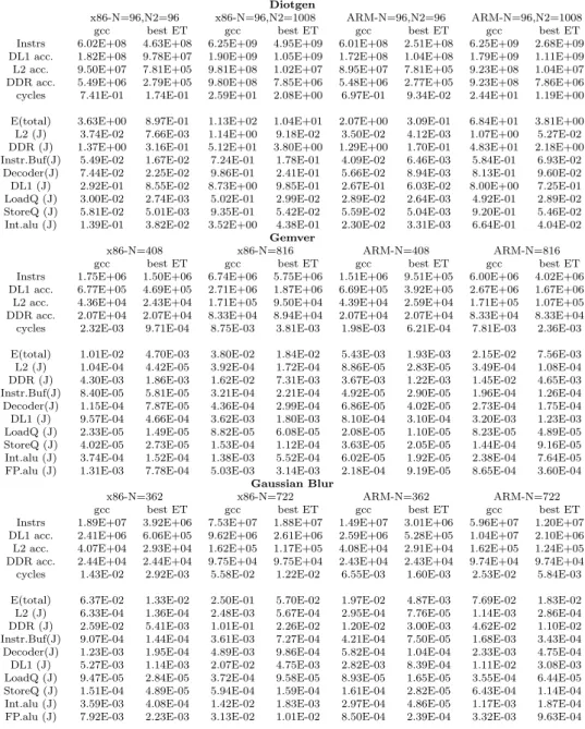
ker-Table 2 Evaluation over gcc using gem5 and mcpat (Diotgen, Gemver and Gaussian Blur)
Diotgen
x86-N=96,N2=96 x86-N=96,N2=1008 ARM-N=96,N2=96 ARM-N=96,N2=1008
gcc best ET gcc best ET gcc best ET gcc best ET
Instrs 6.02E+08 4.63E+08 6.25E+09 4.95E+09 6.01E+08 2.51E+08 6.25E+09 2.68E+09 DL1 acc. 1.82E+08 9.78E+07 1.90E+09 1.05E+09 1.72E+08 1.04E+08 1.79E+09 1.11E+09 L2 acc. 9.50E+07 7.81E+05 9.81E+08 1.02E+07 8.95E+07 7.81E+05 9.23E+08 1.04E+07 DDR acc. 5.49E+06 2.79E+05 9.80E+08 7.85E+06 5.48E+06 2.77E+05 9.23E+08 7.86E+06 cycles 7.41E-01 1.74E-01 2.59E+01 2.08E+00 6.97E-01 9.34E-02 2.44E+01 1.19E+00 E(total) 3.63E+00 8.97E-01 1.13E+02 1.04E+01 2.07E+00 3.09E-01 6.84E+01 3.81E+00 L2 (J) 3.74E-02 7.66E-03 1.14E+00 9.18E-02 3.50E-02 4.12E-03 1.07E+00 5.27E-02 DDR (J) 1.37E+00 3.16E-01 5.12E+01 3.80E+00 1.29E+00 1.70E-01 4.83E+01 2.18E+00 Instr.Buf(J) 5.49E-02 1.67E-02 7.24E-01 1.78E-01 4.09E-02 6.46E-03 5.84E-01 6.93E-02
Decoder(J) 7.44E-02 2.25E-02 9.86E-01 2.41E-01 5.66E-02 8.94E-03 8.13E-01 9.60E-02 DL1 (J) 2.92E-01 8.55E-02 8.73E+00 9.85E-01 2.67E-01 6.03E-02 8.00E+00 7.25E-01 LoadQ (J) 3.00E-02 2.74E-03 5.02E-01 2.99E-02 2.89E-02 2.64E-03 4.92E-01 2.89E-02 StoreQ (J) 5.81E-02 5.01E-03 9.35E-01 5.42E-02 5.59E-02 5.04E-03 9.20E-01 5.46E-02 Int.alu (J) 1.39E-01 3.82E-02 3.52E+00 4.38E-01 2.30E-02 3.31E-03 6.64E-01 4.04E-02
Gemver
x86-N=408 x86-N=816 ARM-N=408 ARM-N=816
gcc best ET gcc best ET gcc best ET gcc best ET
Instrs 1.75E+06 1.50E+06 6.74E+06 5.75E+06 1.51E+06 9.51E+05 6.00E+06 4.02E+06 DL1 acc. 6.77E+05 4.69E+05 2.71E+06 1.87E+06 6.69E+05 3.92E+05 2.67E+06 1.67E+06 L2 acc. 4.36E+04 2.43E+04 1.71E+05 9.50E+04 4.39E+04 2.59E+04 1.71E+05 1.07E+05 DDR acc. 2.07E+04 2.07E+04 8.33E+04 8.94E+04 2.07E+04 2.07E+04 8.33E+04 8.33E+04 cycles 2.32E-03 9.71E-04 8.75E-03 3.81E-03 1.98E-03 6.21E-04 7.81E-03 2.36E-03 E(total) 1.01E-02 4.70E-03 3.80E-02 1.84E-02 5.43E-03 1.93E-03 2.15E-02 7.56E-03 L2 (J) 1.04E-04 4.42E-05 3.92E-04 1.72E-04 8.86E-05 2.83E-05 3.49E-04 1.08E-04 DDR (J) 4.30E-03 1.86E-03 1.62E-02 7.31E-03 3.67E-03 1.22E-03 1.45E-02 4.65E-03 Instr.Buf(J) 8.40E-05 5.81E-05 3.21E-04 2.21E-04 4.92E-05 2.90E-05 1.96E-04 1.26E-04 Decoder(J) 1.15E-04 7.87E-05 4.36E-04 2.99E-04 6.86E-05 4.02E-05 2.73E-04 1.75E-04 DL1 (J) 9.57E-04 4.66E-04 3.62E-03 1.80E-03 8.10E-04 3.10E-04 3.20E-03 1.23E-03 LoadQ (J) 2.33E-05 1.49E-05 8.82E-05 6.08E-05 2.08E-05 1.10E-05 8.23E-05 4.89E-05 StoreQ (J) 4.02E-05 2.73E-05 1.53E-04 1.12E-04 3.63E-05 2.05E-05 1.44E-04 9.16E-05 Int.alu (J) 3.74E-04 1.52E-04 1.38E-03 5.52E-04 6.02E-05 1.92E-05 2.38E-04 7.64E-05 FP.alu (J) 1.31E-03 7.78E-04 5.03E-03 3.14E-03 2.18E-04 9.19E-05 8.65E-04 3.60E-04
Gaussian Blur
x86-N=362 x86-N=722 ARM-N=362 ARM-N=722
gcc best ET gcc best ET gcc best ET gcc best ET
Instrs 1.89E+07 3.92E+06 7.53E+07 1.88E+07 1.49E+07 3.01E+06 5.96E+07 1.20E+07 DL1 acc. 2.41E+06 6.06E+05 9.62E+06 2.61E+06 2.59E+06 5.28E+05 1.04E+07 2.10E+06 L2 acc. 4.07E+04 2.93E+04 1.62E+05 1.17E+05 4.08E+04 2.91E+04 1.62E+05 1.24E+05 DDR acc. 2.44E+04 2.44E+04 9.75E+04 9.75E+04 2.43E+04 2.43E+04 9.74E+04 9.74E+04 cycles 1.43E-02 2.92E-03 5.58E-02 1.22E-02 6.55E-03 1.60E-03 2.53E-02 5.84E-03 E(total) 6.37E-02 1.33E-02 2.50E-01 5.70E-02 1.97E-02 4.87E-03 7.69E-02 1.83E-02 L2 (J) 6.33E-04 1.36E-04 2.48E-03 5.67E-04 2.95E-04 7.76E-05 1.14E-03 2.86E-04 DDR (J) 2.59E-02 5.41E-03 1.01E-01 2.26E-02 1.20E-02 3.00E-03 4.62E-02 1.10E-02 Instr.Buf(J) 9.07E-04 1.44E-04 3.61E-03 7.27E-04 4.21E-04 7.50E-05 1.68E-03 3.43E-04 Decoder(J) 1.23E-03 1.95E-04 4.89E-03 9.86E-04 5.82E-04 1.04E-04 2.33E-03 4.75E-04 DL1 (J) 5.27E-03 1.14E-03 2.07E-02 4.75E-03 2.82E-03 8.39E-04 1.11E-02 3.08E-03 LoadQ (J) 9.47E-05 2.84E-05 3.72E-04 9.58E-05 8.93E-05 1.65E-05 3.55E-04 6.44E-05 StoreQ (J) 1.51E-04 4.89E-05 5.94E-04 1.59E-04 1.61E-04 2.82E-05 6.43E-04 1.14E-04 Int.alu (J) 3.59E-03 4.08E-04 1.42E-02 1.83E-03 2.97E-04 4.86E-05 1.17E-03 1.87E-04 FP.alu (J) 7.92E-03 2.23E-03 3.13E-02 1.01E-02 8.50E-04 2.39E-04 3.32E-03 9.63E-04
nel code and as a consequence the error values. This disunion refers only to cases that the tile size of the innermost iterator is twice its minimum value; in that case the compiler is likely to fully unroll that loop, affecting the code. Thus, this case has to be included to the first branch in Step 6 (Algorithm 1).