Substrate Integrated Waveguide Based Millimeter Wave Antennas
Dhruva Kumar Chandrappa
A Thesis In the Department
of
Electrical and Computer Engineering
Presented in Partial Fulfillment of the Requirements For the Degree of
Master of Applied Science (Electrical and Computer Engineering) at Concordia University
Montreal, Quebec, Canada
October 2019
CONCORDIA UNIVERSITY School of Graduate Studies
This is to certify that the thesis prepared By: Dhruva Kumar Chandrappa
Entitled: Substrate Integrated Waveguide Based Millimeter Wave Antennas and submitted in partial fulfillment of the requirements for the degree of
Master of Applied Science (Electrical and Computer Engineering)
complies with the regulations of the University and meets the accepted standards with respect to originality and quality.
Signed by the final examining committee:
Chair and Examiner Dr. Robert Paknys
External to Program Dr. Alexey Kokotov
Thesis Supervisor Dr. Abdel Razik Sebak
Approved By:
Dr. Rastko Selmic, Graduate Program Director
November 6, 2019
Dr. Amir Asif, Dean
Abstract
Substrate Integrated Waveguide Based Millimeter Wave Antennas Dhruva Kumar Chandrappa
Concordia University, October 2019
Antennas those operating at millimeter-wave (mm-wave) frequencies (30 - 300 GHz) are more advantageous than operating at less than 6 GHz, due to a reduction in antenna physical dimensions, an increase in the data transfer rate, and reduction in latency. How-ever, the electromagnetic waves propagating in free-space at mm-wave frequencies experience significant propagation path loss due to the atmospheric absorption and rain attenuation. Therefore, high-gain antennas are preferred to compensate for path loss and to increase the range of wireless communication. Also, transmission lines such as microstrip, and coplanar waveguides incur high radiation losses at mm-wave frequencies. Hence, to minimize losses, a planar waveguide known as a substrate integrated waveguide (SIW) is preferred. Besides, at mm-wave frequencies, circularly polarized (CP) waves are preferred over linearly polarized (LP) waves as these waves reduce multi-path effects at the receiver.
The objectives of this thesis are to design high-gain linearly, and circularly polarized antennas based on SIW at the mm-wave frequency 30 GHz. The proposed antenna models were designed, simulated, and analyzed using CST software. The antenna prototypes were fabricated and measured for the reflection coefficient, gain, and principal plane radiation patterns. In this thesis, we are proposing two single element antennas, a linear to circular wave polarizer, and an array antenna.
At first, we present, a planar, cylindrical sector-substrate integrated waveguide (CS-SIW) narrow slot antenna. The impedance bandwidth of this antenna is 10.87% which is approximately equivalent to 4 GHz of bandwidth at 30 GHz, and the antenna gain ranges from 8.33 to 8.84 dB within the impedance bandwidth. Further, to improve the gain, an engineered substrate is constructed on top of the CS-SIW slot antenna. The impedance bandwidth of the modified antenna is 10.42% - also, the gain ranges from 10.5 to 11.44 dB over the impedance bandwidth, which implies an increase in the gain from 2.1 to 2.7 dB when compared with the gain of CS-SIW slot antenna. Also, we propose a three-layered meander-line polarizer at 30 GHz which transforms linearly polarized waves to circularly polarized waves for the CS-SIW slot antenna.
Lastly, we present, a 1 × 8 CS-SIW slot antenna array with a superstrate to achieve a high-gain LP antenna. The impedance bandwidth of the antenna is 10%. The gain of the array antenna integrated with a superstrate layer varies from 21.35 to 22.95 dB over the impedance bandwidth.
Acknowledgments
I would like to express my sincere gratitude to my advisor Dr. Abdel Razik Sebak for the continuous support and encouragement throughout the MASc. program. I would also like to thank both the committee members Dr. Robert Paknys and Dr. Alexey Kokotov for reviewing the manuscript, and their valuable feedback.
Also, I would like to thank Mr. Traian Antonescu (Polytechnique Montreal University) for fabricating all the antenna prototypes mentioned in this document. And, Mr. Maxime Thibault (Polytechnique Montreal University) and Mr. Vincent Mooney-Chopin (Concordia University) for their help on antenna radiation pattern measurements.
I would like to extend my thanks to all my beloved friends and colleagues namely (in no particular order): Ali, Nadeem, Shraman, Sifat, and Yazan — for all our (non) technical discussions, and for making the workplace lively and memorable.
Lastly, but not the least, I would like to take this opportunity to thank my family wholeheartedly for all their unconditional love and support.
Table of Contents
List of Figures x
List of Abbreviations xv
Chapter 1: Introduction 1
1.1 Motivation and Problem Statement . . . 3
1.2 Objectives . . . 4
1.3 Theoretical Background and Design Methodology . . . 4
1.4 Thesis Outline . . . 6
Chapter 2: Background 7 2.1 Introduction . . . 7
2.2 Slot Antenna . . . 7
2.3 Complementary Antennas: Babinet’s Principle . . . 9
2.4 Substrate Integrated Waveguide (SIW) . . . 10
2.5 SIW based Slot Antennas . . . 14
2.5.1 Linearly Polarized Antennas . . . 14
2.5.2 Circularly Polarized Antennas . . . 16
Chapter 3: The Linear and Circular Polarized Cylindrical Sector (CS)-SIW Narrow Slot Antenna 19 3.1 Introduction . . . 19
3.2.1 Cylindrical Sector Substrate Integrated Waveguide (CS-SIW) . . . 20
3.2.2 SIW to CS-SIW . . . 21
3.2.3 Microstrip Line to SIW . . . 21
3.3 Results and Discussion . . . 23
3.4 Proposed LP CS-SIW Narrow Slot Antenna for Gain Improvement . . . 28
3.4.1 Design of EBG Unit Cell . . . 28
3.4.2 Results and Discussion . . . 30
3.5 Comparsion With Other mm-wave Antennas . . . 33
3.6 Proposed CP CS-SIW Narrow Slot Antenna using Meander-line Polarizer . . 35
3.6.1 Introduction . . . 35
3.6.2 Theory of Meander-line Polarizer . . . 36
3.6.3 Design of Meander-line Polarizer Unit Cell . . . 37
3.6.4 Design and Analysis of CS-SIW Slot Antenna using Meander-line Po-larizer . . . 40
3.6.5 Results and Discussion . . . 41
3.7 Summary . . . 45
Chapter 4: The Linear Eight Element LP CS-SIW Narrow Slot Antenna Array 47 4.1 Introduction . . . 47
4.2 Design of 1×8 SIW Power Divider . . . 47
4.3 Design of 1×8 LP CS-SIW Narrow Slot Antenna Array . . . 49
4.4 Results and Discussion . . . 50
4.6 Results and Discussion . . . 55 4.7 Summary . . . 58
Chapter 5: Conclusion 60
5.1 Future Work . . . 61
List of Figures
1.1 Representation of WLAN and WPAN for indoor environment. The coverage area for WLAN is between 10 - 100 m, and WPAN is<10 m (see [3], fig. 1.7,
1.9). . . 2
1.2 (a) Plot of expected atmospheric absorption loss (in dB/km) versus frequency (in GHz) [5]. (b) Plot of rain attenuation (in dB/km) versus frequency (in GHz) at multiple rain velocities (in mm/hr) [5]. . . 3
1.3 Flowchart of antenna design methodology. . . 5
2.1 (a) A slot on an infinite conductor sheet. (b) Illustration of the normalized voltage distribution inside the slot for slot lengths, l, equal to λ/2 and 3λ/2. 8 2.2 A slot antenna and its complementary structure, a dipole antenna. Air is replaced with conductor, and conductor is replaced with air to obtain com-plementary antenna. . . 10
2.3 PrincipalE andH radiation patterns for the slot and dipole antenna oriented along xaxis. . . 10
2.4 3D model of rectangular waveguide. . . 11
2.5 (a) 3D model of an uniform SIW and its dimensions are h = 0.508, d = 0.4, p= 0.8 and a= 5 (all are in mm); (b) S-parameters of a two-port reciprocal uniform SIW model; (c) Top view of |E| field (V/m) inside uniform SIW, normal toz; and, (d) Top View of|H|field (A/m) inside uniform SIW, normal toz. . . 13
2.6 SIW cavity backed planar slot antenna (redrawn from [12]). . . 14
2.7 SIW cavity backed bow-tie slot antenna (redrawn from [13]). . . 15
2.9 A SIW cavity backed wide slot antenna array consisting of 2×4 elements (redrawn from [12]). . . 16 2.10 High gain planar array antenna designed at 60 GHz (redrawn from [16]). . . 16 2.11 SIW cavity backed crossed slot antenna (redrawn from [17]). . . 17 2.12 Wideband circularly polarized SIW cavity-backed antenna (redrawn from [18]). 17 2.13 Three layered SIW cavity based CP antenna (redrawn from [19]). . . 18 3.1 3D view of CS-SIW narrow slot antenna and its corresponding dimensions (in
mm) are: h = 0.508, a = 5, b = 15.78, c= 6, e = 13.6, f = 28.08, g = 19.2,
k= 1.31, l = 14, m= 1.28 and φ= 67◦. . . . 20
3.2 (a) Normalized standing wave pattern of the electric field intensity, |E|, (in V/m) inside CS-SIW at 30 GHz; (b) Normalized standing wave pattern of the magnetic field intensity, |H|, (in A/m) inside CS-SIW at 30 GHz. . . 22 3.3 MS-SIW-MS transition (a) 3D view and its corresponding dimensions (in mm)
are a = 5, b = 1.7, d = 0.4, h = 0.508, p = 0.8 and m = 1.28 (b) Plot of two-port scattering parameters (in dB) versus frequency (in GHz). . . 23 3.4 (Top) The top-view of CS-SIW narrow slot antenna prototype. (Bottom) The
CS-SIW narrow slot antenna, antenna under test (AUT), for radiation pattern measurement inside the anechoic chamber. . . 24 3.5 LP CS-SIW narrow slot antenna (a) plot of simulated |S11| (in dB) and
real-ized gain (in dB) versus frequency (in GHz) for ǫr = 2.94 ; and, (b) plot of
simulated |S11| (in dB) and realized gain (in dB) versus frequency (in GHz) for ǫr= 2.7. . . 25
3.6 (a) and (b) Plot of complex input impedance (in Ω) versus frequency (in GHz), (c) plot of normalized electric field intensity, Ey, (in V/m) inside the
slot versus slot length, l, (in mm) at various frequencies, and (d) plot of impedance bandwidth (in %) versus slot length, l, (in mm). . . 26
3.7 Measured (dotted) and simulated (dashed) normalized radiation patterns (E -plane (φ = 90◦) and H-plane (φ = 0◦)) for CS-SIW narrow slot antenna at
multiple frequencies. . . 27 3.8 Multilayer CS-SIW narrow slot antenna for improving gain and its
corre-sponding dimensions (in mm) are: a1 = 1.28, b1 = 0.508, c1 = 6, d1 = 14.4,
f1 = 1.31, h1 = 14, g1 = 15.87, e1 = 35.29, c2 = 0.787, d2 = 10.8, a2 = 15.5,
b2 = 6, e2 = 24, f2 = 19.2, g2 = 2.4, andφ = 67◦. . . . 29
3.9 (a) Top and Side view of the designed EBG unit cell and its corresponding dimensions (in mm) arec= 2.4, d= 0.787 and e= 2 (b) Dispersion diagram for the designed and simulated EBG unit cell. The band-gap phenomenon is observed from 20 - 35 GHz. . . 30 3.10 (Top) The top-view of the multi-layer CS-SIW narrow slot antenna prototype.
(Bottom) The multi-layer CS-SIW narrow slot antenna for radiation pattern measurement inside the anechoic chamber. . . 31 3.11 (a) Plot of simulated and measured reflection coefficient, |S11|, (in dB) and
realized gain (in dB) versus frequency (in GHz) for the CS-SIW narrow slot antenna gain improvement; and (b) Comparison between simulated and mea-sured realized gain (in dB) versus frequency (in GHz) for with and without top layer. . . 32 3.12 Measured (dotted) and simulated (dashed) normalized radiation patterns (E
-plane (φ = 90◦) and H-plane (φ = 0◦)) for CS-SIW slot antenna gain
im-provement at multiple frequencies. . . 33 3.13 Normalized equivalent transmission line model for the three layer stacked
meander-line polarizer, wherey0 =Y0/Y0 = 1,jbm =jBm/Y0, andynin=Yinn/Y0. 36
3.14 Three layered meander-line equivalent circuit analysis at center frequency, f0, using admittance Smith chart for inductive susceptances, jb1, jb2 and jb3. . . 37
3.15 (a) 3D view of three layered meander-line polarizer unit cell. ‘UCB’ represent ‘Unit Cell Boundary’ and ‘FP’ represent ‘Floquet Port’, (b) Amplitude ratio and phase difference (in degree) of TE, TM mode versus frequency (in GHz), (c) Top and bottom layer of the designed unit cell, and (d) Middle layer of the designed polarizer unit cell. Meader-line polarizer’s unit cell dimension’s (in mm) are: a = 4.15, b = 0.2, c = 0.9, d = 0.35, e = 1.8, f = 2.075, and
φ= 45◦. . . . 38
3.16 Three layered meander-line polarizer unit cell (a) plot of|TE|,|TM|reflection and transmission coefficients versus frequency (in GHz); (b) plot of TE and TM transmission coefficients phase (in deg) versus frequency (in GHz). . . . 39 3.17 3D view of circularly polarized CS-SIW slot antenna using meander-line
po-larizer. And, the corresponding antenna dimension’s (in mm) are as follows:
ps= 2.5, pt= 0.254, ph= 4.02, pl= 39.11, w= 45.2 andl = 45.2. . . 40 3.18 Individual layers of the CS-SIW narrow slot antenna using meander-line
po-larizer. . . 42 3.19 (Left) The circularly polarized CS-SIW narrow slot antenna prototype.
(Cen-ter) front view of the polarizer antenna. (Right) The circularly polarized CS-SIW narrow slot antenna for radiation pattern measurement inside the anechoic chamber. . . 43 3.20 Plot of axial ratio (in dB) versus Frequency (in GHz) for different separation
height between CS-SIW narrow slot antenna and meander-line polarizer, ph, (in mm). . . 43 3.21 CS-SIW narrow slot antenna using meander-line polarizer (a) plot of reflection
coefficient,|S11|, (in dB) and realized gain (in dB) versus frequency (in GHz); (b) Plot of axial ratio (in dB) versus frequency (in GHz). . . 44 3.22 Electric field (in V/m) vector plot at 31 GHz (and fixed distance, z). . . 44 3.23 Plot of measured (dotted) and simulated (dashed) normalizedE-plane andH
-plane radiation patterns atφ= 90◦ for a CS-SIW slot meander-line polarizer
4.1 Top view of the symmetrical nine port matched SIW power divider and its dimensions (in mm) are a = 33.174, b = 1.8, c = 16.6, d = 66, e = 16.58,
f = 5 and h= 34.377. . . 48 4.2 Plot of SIW power divider scattering parameters (a) reflection coefficient (in
dB) with respect to frequency (in GHz); and (b) transmission coefficients (in dB) with respect to frequency (in GHz). . . 49 4.3 3D view of eight element linear CS-SIW slot array antenna and its
correspond-ing dimensions (in mm) arel = 64.27, w= 135.26 and h= 0.544. . . 50 4.4 (Top) The 1×8 CS-SIW narrow slot antenna array prototype. (Bottom) the
1×8 CS-SIW narrow slot antenna array for radiation pattern measurement inside the anechoic chamber. . . 51 4.5 Plot of simulated and measured eight element linear CS-SIW slot array
an-tenna for (a) reflection coefficient, |S11|, (in dB) versus Frequency (in GHz); and (b) realized gain (in dB) versus Frequency (in GHz). . . 52 4.6 Comparison plot of measured realized gain (in dB) between CS-SIW single
element and eight-element linear CS-SIW slot array antenna versus frequency (in GHz). . . 53 4.7 Measured (dotted) and simulated (dashed) normalized radiation patterns (E
-plane (φ = 90◦) and H-plane (φ = 0◦)) for an eight-element linear CS-SIW
slot array antenna at multiple frequencies. . . 54 4.8 3D view of eight-element linear CS-SIW slot array antenna with superstrate
and its corresponding dimensions (in mm) aresl = 135.26,sw= 17.2,h= 5.4,
st= 0.64 andl = 64.27. . . 55 4.9 (Top) The 1×8 CS-SIW narrow slot antenna array prototype with superstrate.
(Bottom) The 1×8 CS-SIW narrow slot antenna array with superstrate for radiation pattern measurement inside the anechoic chamber. . . 56 4.10 Measured and simulated plots for eight-element linear CS-SIW slot array
an-tenna with superstrate (a) reflection coefficient,|S11|, (in dB) versus frequency (in GHz); and (b) realized gain (in dB) versus frequency (in GHz). . . 57
4.11 Measured (dotted) and simulated (dashed) normalized radiation patterns (E -plane (φ = 90◦) and H-plane (φ = 0◦)) for an eight-element linear CS-SIW
slot array antenna with superstrate at multiple frequencies. . . 58 4.12 Measured and simulated comparison plots between eight-element linear
CS-SIW slot array antenna with and without superstrate (a) realized gain (in dB) versus frequency (in GHz); and (b)H-plane SLL (in dB) versus frequency (in GHz). . . 59
List of Abbreviations
AMC artifical magnetic conductor
CP circular polarization
CS-SIW cylindrical sector substrate integrated waveguide CST Computer Simulation Technology
DTR data transfer rate
EBG electromagnetic bandgap
EM electromagnetic
FTBR front to back ratio
GCPW grounded coplanar waveguide LHCP left-hand circular polarization
LNA low noise amplifier
LOS line of sight
LP linear polarization
mm-wave millimeter-wave
NLOS non-line of sight
PA power amplifier
PCB printed circuit board
PMC perfect magnetic conductor RHCP right-hand circular polarization
SIR signal to interference ratio SIW substrate integrated waveguide
SLL side lobe level
TE transverse electric
TEM transverse electromagnetic
TM transverse magnetic
Tx transmitter
UE user equipment
UHF ultra high frequency
VNA vector network analyzer
WLAN wireless local area network WPAN wireless personal area network
Chapter 1: Introduction
Wireless communication has seen tremendous growth in the modern world. Therefore, wireless application ranges from defense to medical industries (see [1], p.116). An antenna is a backbone for the existence of any wireless communication. Antennas are designed, tuned to operate at the dedicated frequency (which imply, a wireless device operates at that frequency), and their properties differ from application to application. Each wireless device consists of an antenna; to transmit (or receive) electromagnetic (EM) waves to (or from) free-space (see [2], p.1-4). The radiated EM waves carry information while propagating in free-space and thus enabling wireless communication link between transmitter and receiver. The most popular wireless networks are a cellular network, wireless local area network (WLAN), and wireless personal area network (WPAN). Due to a large number of users often use user equipment (UE) devices to transmit and receive information, as shown in figure 1.1. UE devices, to name a few, are cellular phones, tablets, smart-watch. As the number of UE devices per person increases, the number of links has to be interlinked with the access points such as Wi-Fi, for wireless communication to be successful. Scaling the above scenario to thousands of users leads to a myriad of wireless links, e.g., at densely populated areas. At this instance - users experience high latency, decrease in service quality, and unstable wireless connectivity.
Increasing channel bandwidths can solve the above challenges for each wireless applica-tion (see [3], p.14). However, for frequencies less than 6 GHz, the frequency spectrum is overcrowded by a diversity of wireless applications, which mean, wide channel bandwidths are unfeasible (see [3], p.3), [4].
The search for the availability of wide channel bandwidths is scanned across the frequency spectrum and found at millimeter-wave (mm-wave) frequencies. The mm-wave frequency ranges from 30 - 300 GHz, and the corresponding free-space wavelength,λ0 =c/f, is between 10 - 1 mm, respectively (where cis the speed of light and is ≃ 3 ×10⁸ m/s). Currently, the
only applications operating at wave are military and radar. Hence, most of the mm-wave frequency spectrum is unused, and wide bandwidths are feasible. For instance, 1 GHz of bandwidth is readily available at frequencies 28 GHz and 38 GHz (see [3], p.5).
' ' ' ' ' ' ' ' ' ' ' ' ' ' ' ' ' ' ' ' ' ' W L A N W P A N Wire Internet
Figure 1.1: Representation of WLAN and WPAN for indoor environment. The coverage area for WLAN is between 10 - 100 m, and WPAN is <10 m (see [3], fig. 1.7, 1.9).
At mm-wave frequencies, the EM wave propagating in free space experience path loss due to atmospheric absorption and rain attenuation as free space wavelengths are shorter in the order of millimeters. The plot of atmospheric absorption loss (in dB/km) and rain attenuation (dB/km) for multiple rain velocity versus frequency (in GHz) are shown in figure 1.2(a) and 1.2(b). As read from figure 1.2, the combined atmosphere and rain attenuation losses (assuming high rain velocity) increases as frequency increases. Therefore, the long-range wireless communication system is not suitable at mm-wave frequencies.
However, to overcome the propagation path loss, two solutions can be employed: (a) to reduce the distance between the transmitter and receiver to about less than 200 m [4, 5]. For instance, at 28 GHz, the atmospheric absorption is equal to 0.012 dB, and the rain attenuation is equal to 1.4 dB for hefty rainfall (of 25 mm/hr). Therefore, the number of base stations supporting cellular networks increases drastically from today’s base stations, which are operating below 6 GHz. (b) to design and build a high gain antenna system that can overcome the barrier of propagation path loss and still would be sufficient to cover long-range distances.
50 100 150 200 250 300 10−2 10−1 100 101 102 Frequency (GHz) E x p ec te d at m . lo ss (d B /k m ) 100 101 102 10−3 10−2 10−1 100 101 102 Frequency (GHz) R ai n at tn . (d B /k m ) 150100 50 25 5 1.25 0.25 (a) (b)
Figure 1.2: (a) Plot of expected atmospheric absorption loss (in dB/km) versus frequency (in GHz) [5]. (b) Plot of rain attenuation (in dB/km) versus frequency (in GHz) at multiple rain velocities (in mm/hr) [5].
1.1
Motivation and Problem Statement
At mm-wave frequencies, free-space propagation path loss dominates (see [3], pg.100). Therefore, to overcome path loss, a high-gain (directional) antennas must be employed to communicate over a long distance. In general, for an antenna to radiate efficiently - the antenna size should be comparable to its operating wavelength, for example, a resonant dipole antenna. By taking advantage of this fact, an antenna operating at mm-wave frequency occupies small area (thus, less resource) when compared to antennas operating at UHF or below (more resource).
At mm-wave frequencies and beyond, unbounded transmission lines such as microstrip, coplanar waveguide, exhibit high radiation losses; and has low power handling capability. Therefore, to overcome these challenges, a planar waveguide such as a substrate integrated waveguide (SIW) is preferred.
At mm-wave frequencies, linearly polarized waves are susceptible to multi-path due to a reflective materials readily available in the environment [4]. Multi-path is observed at the receiver when a line of sight (LOS) signal and non-line of sight (NLOS) signal arrive at the same time with different phases. Thus, when an antenna radiates linearly polarized waves there are higher chances that the phase of the LOS and NLOS signals are out of phase with
each other. Therefore, the receiver must be able to use all the resources to identify and process the signal. However, by using a circularly polarized antenna, multi-path effects can be reduced (see [1], p.120).
1.2
Objectives
High-gain antennas overcome the difficulties mentioned in section 1.1. The main objective of this thesis is to design high-gain linearly, and circularly polarized antennas based on SIW at 30 GHz and includes the following two main tasks:
1. To design, simulate, fabricate, and measure a low-profile planar antenna element at the center frequency, fc, equal to 30 GHz. Also, to design a wideband standalone polarizer
which can transform linearly polarized waves radiating from an antenna to circularly polarized waves at fc.
2. To design design, simulate, fabricate, and measure a high gain antenna array system atfc.
1.3
Theoretical Background and Design Methodology
The purpose of an antenna is to send and receive EM waves. However, these waves are both direction and polarization dependent which are spatially distributed over a spherical coordinate system surrounding the antenna. As a result, to understand visually, we can sketch the principal E plane and H plane radiation patterns of an antenna on a 2D polar plot. These principal patterns depend on the distribution of time-varying currents on the antenna physical aperture. Therefore, the calculation for the total current distribution on the antenna aperture is imperative. Not all antenna apertures are as simple as a resonant dipole antenna. Therefore, rigorous and complex numerically methods should be incorporated for complex apertures in order to calculate currents. Some of the numerical methods to name a few are FDTD (Finite-Difference Time-Domain), FEM (Finite Element Method), MoM (Method of Moments) (see [1], Chap 14).
Material selection
(relative permittivity and thickness of a dielectric substrate)
Antenna modelling using CST-MS software (geometry, radiating element, feeding structure)
Define port, and boundary conditions (if any)
Full wave analysis by choosing a suitable solver and optimization (transient solver, eigenmode solver)
Antenna fabrication
Fabricated antenna measurements (VNA, anechoic chamber)
Figure 1.3: Flowchart of antenna design methodology.
Design Methodology
The antenna design methodology involves the selection of a suitable dielectric substrate to fabricate SIW structures. Furthermore, the substrate thickness and relative permittivity are crucial for designing an antenna. The model of an antenna is constructed using commercial software such as CST, followed by defining the port and boundary conditions. The port acts as a signal source for an antenna. The full-wave analysis of the designed antenna model is carried out by choosing the appropriate solver such as time-domain or frequency-domain solver. The eigen mode solver perform the analysis of periodic structures in CST. The CST utilizes FDTD numerical technique to obtain a solution to the designed model. The results of a solution, to name a few are reflection coefficient, radiation patterns, gain estimation, efficiency. Further, if necessary, the model parameters are optimized to achieve satisfactory results.
model is fabricated and measured. The reflection coefficient of the antenna model is mea-sured using a vector network analyzer, while the antenna radiation patterns are meamea-sured using an anechoic chamber. Figure 1.3 depicts the design methodology flowchart. In this flowchart, most of the steps remain unchanged for various antenna problems except the antenna modeling (i.e., step 2).
1.4
Thesis Outline
Chapter 2 covers the literature survey. We begin with the theoretical understanding of the slot antenna and introduce the concept of complementary antennas. Also, it includes design, theory, and analysis of the SIW structure. In Chapter 3, we propose three single element antennas at 30 GHz. These antennas radiate LP waves. Also, by designing a meander-line polarizer, the transformation of LP waves to CP waves is shown. In Chapter 4, we present a high-gain antenna array system by designing a SIW corporate feeding network. At last, in Chapter 5, we conclude the thesis with a summary and discuss the feasibility of extending this work in the future.
Chapter 2: Background
2.1
Introduction
Planar antennas (such as slot or patch antenna) are profile, light-weight, and low-cost antennas. These antennas can be easily integrated with the other RF components (such as amplifiers, filters, switches) on a printed circuit board (PCB) to build a transceiver. As a result, planar antennas are preferred in various applications, to name a few, aircraft, spacecraft, satellite, cellular phones - owing to their low-profile nature (see [6], chap.12 and 14). Therefore, in this thesis, our dedication was inclined towards slot antenna based on substrate integrated waveguide (SIW) technology.
In this chapter, we begin with a discussion on the theoretical analysis of slot antennas. It is followed by an explanation of complementary structures and usefulness of Babinet’s Principle. Later, planar form of dielectric rectangular waveguide known as substrate inte-grated waveguide (SIW) is discussed. Also, we shall present a few existing SIW slot antennas available in the literature.
2.2
Slot Antenna
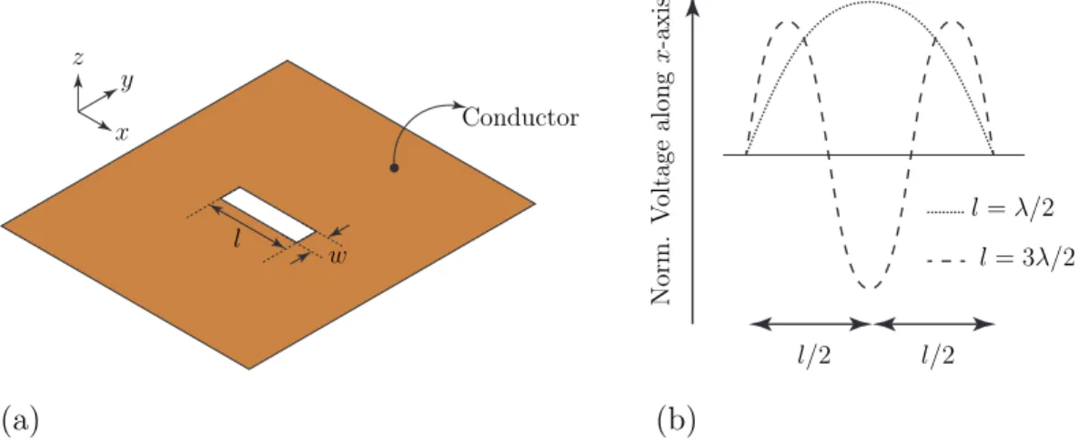
The slot antenna belongs to a family of aperture antennas. Aperture antennas are anten-nas in which the EM waves radiate from the aperture or an opening. A few other examples for aperture antenna include horn, lens, reflector, and surface-wave antennas. A slot antenna is the simplest of all aperture antennas to design and construct. And, is realized by etching a slot on an infinite conductor such as aluminum or copper as shown in figure 2.1. Since aircraft’s and spacecraft’s outer body is a conductor, slot antennas can be flush-mounted on the conductor surface and are thus preferred for space applications.
Let us now assume that the infinitely extending infinitesimal thickness conductor (in-cluding slot) is dividing the whole region into two halves at the origin as shown in figure 2.1. Let, z < 0 denote medium-1 consisting of air. Similarly, z > 0 denotes medium-2
x y z l w Conductor l=λ/2 l= 3λ/2 l/2 l/2 N or m . V olt ag e alo n g x -a x is (a) (b)
Figure 2.1: (a) A slot on an infinite conductor sheet. (b) Illustration of the normalized voltage distribution inside the slot for slot lengths, l, equal toλ/2 and 3λ/2.
which is source-free and consisting of air. For an EM wave traveling from medium-1 towards medium-2, it has to pass via slot with dimensions l×w. The infinite conductor acts as a short circuit (barrier) and thus won’t let any field to penetrate through it. Therefore, the size and the shape of the slot on the conductor determines the quantity of field in medium-2. For instance, if we cover the slot area by using a conductor, no wave can propagate to medium-2 (field-free behavior still exists). Further extending the above concept to slot as an antenna, the shape and size of the aperture or slot are frequency-dependent quantities that help to determine the center frequency, input impedance and polarization of the EM field in medium-2.
To understand the behavior of a slot antenna in terms of voltage and current, let us connect an AC signal source to the slot narrow wall along the y axis at position l/2 shown in figure 2.1(a). We also assume that the slot length, l, is equal to λ0/2 and slot width, w, is w ≪ λ0. The analogy is similar to the transmission line terminated with short circuit load at distance λ0/4 from the source. We can now solve this problem by using transmission line analysis inside the slot. We can calculate that, the voltage is maximum at the center of the slot, and minimum at the ends of the slot as shown in 2.1(b) for l =λ0/2. However, the current is minimum at the center of the slot, and maximum at the ends of the slot. In addition, the currents are out of phase at the ends of the slot along the x axis. When the impedance of the AC source is matched with the impedance of slot antenna at resonance, the slot antenna radiates EM field on either side of the conductor (i.e., +z and−z axis) due to the in phase distribution of the voltage along thex axis.
To determine the specific radiated fields from the slot antenna, we need to know the value of surface current distribution on the conductor. For instance, for wire antennas (such as dipole antenna) the impressed current density, J, exists only on the wire. We can calculate vector potential, A, using J. The magnetic field, H, can be calculated using A and subsequently, E, from H using Maxwell’s curl equation (see [7], sec 4.1). We can follow a similar procedure for slot or aperture antennas to calculate the radiated fields by knowing the surface current. When the AC signal is applied to the slot as shown in figure 2.1, the impressed currents travel across the conductor and won’t refrain well within the slot. However, if the conductor extends over infinite distances, we can make use of image theory for simplification [1]. However, infinite structures are not realizable. Another approach is to evaluate the field over the slot alone, rather than considering the abundance of a conductor. The curling electric fields are replaced with magnetic current density, M, along the length of the slot. If the specific fields were known at every point on the face of the slot, we can calculate radiated fields from the slot.
2.3
Complementary Antennas: Babinet’s Principle
Consider a slot antenna, as shown in figure 2.1. If we were to replace the conductor with air and fill the slot with a conductor, we would achieve slot antennas dual structure. In this case, it is a dipole antenna. Thus, both slot and dipole antennas are said to be complementary antennas, as shown in figure 2.2. In 1946, Booker derived an equation between the impedance of the slot and dipole antenna considering polarization using Babinet’s principle [8] (see [6], sec 12.8).
Since dipole antennas are easily understood and analyzed, using Babinet’s principle, we can readily calculate the impedance of the slot antenna. IfZslot is the impedance of the slot
antenna and Zdipole is the impedance of the dipole antenna, then by Babinet’s principle:
ZslotZdipole =
η2
4 (2.1)
Where η is the intrinsic impedance of the ambient medium of complementary antennas. If air is the ambient medium, η = η0 = 377 Ω
Further, Babinet’s principle tells us if the radiation pattern of an antenna is known, the radiation pattern for its dual antenna can be obtained by interchanging principal E plane
x y z
Slot Antenna Dipole Antenna
Conductor
Air
Figure 2.2: A slot antenna and its complementary structure, a dipole antenna. Air is replaced with conductor, and conductor is replaced with air to obtain complementary antenna.
Slot antenna
Dipole antenna
E-plane (θ= 90◦) H-plane (φ= 90◦)
Gain (max)
Gain (min)
Figure 2.3: Principal E and H radiation patterns for the slot and dipole antenna oriented along x axis.
and H plane radiation patterns. Therefore, for an x-directed dipole and slot antenna shown in figure 2.2, we can plot the principalE plane and H plane radiation patterns as illustrated in figure 2.3.
2.4
Substrate Integrated Waveguide (SIW)
A waveguide is a 3-D structure which guides an EM wave from one point to another. A waveguide can be hollow or filled with a dielectric substrate bounded by a conductor. The
x y z a
b
t ǫr
Figure 2.4: 3D model of rectangular waveguide.
for the wave propagating inside the waveguide is zero. Because when the wave interacts with the air-conductor interface, the wave reflects inside the waveguide; enforcing air-conductor boundary conditions assuming the conductor thickness is much larger than the skin depth. In addition, the attenuation loss in a waveguide is frequency-dependent and increases as the frequency increases. For example, for the rectangular waveguide (WR) operating in T E10
mode and constructed with copper, the losses using (see [9], eq. 3.96) are 0.576 dB/m for WR-28 at 32 GHz, and 1.51 dB/m for WR-15 at 60 GHz.
Waveguides can take many shapes due to their 3-D structure. To differentiate between several waveguides, we can prefix the waveguide depending on the shape of the waveguide cross-section. Thus, the rectangular waveguide has a cross-section in the shape of a rectangle. Likewise, the circular waveguide has a circular cross-section and so on. The 3-D model of the hollow (ǫr = 1) rectangular waveguide with conductor thickness, t, is shown in figure
2.4. The waveguide cross-section is in the xy plane, and the dimensions area and b (where
a > b) along x and y, respectively. Also, the waveguide longitudinal (or wave propagation direction) is along the z axis. In general, a waveguide supports transverse electric (TE) or transverse magnetic (TM) waves. However, the propagation of a transverse electromagnetic (TEM) wave is not possible inside the waveguide due to unsatisfied boundary conditions at the cross-section of the conductor perimeter.
Since we are interested in the planar form of waveguide (such as SIW), the derivation and analysis on the conventional rectangular or circular waveguide is out of scope from this thesis, and one can refer to (see [7], chap.3).
Substrate Integrated Waveguide (SIW)
The excitation of the slot antenna driven by an AC source (figure 2.1) is delicate at the intersection of the source terminals and conductor. Therefore, we have to replace the AC source by introducing a feeding mechanism that can excite the slot and also provide similar behavior as the source. Since we are interested in designing planar antennas, preference is given to planar feeding structure rather than rectangular waveguide, as shown in figure 2.4. Examples of planar feeding structure include, but not limited to, microstrip, stripline, SIW, grounded coplanar waveguide (GCPW). Microstrip feeding structure is one of the famous transmission lines and easy to design. However, the preferred choice of SIW as a feeding structure over microstrip is because of SIW exhibit high-quality factor, power handling, elimination of surface waves, and low attenuation losses as frequency increases at Ka-band. The disadvantages of SIW over microstrip include ease of fabrication, low bandwidth, and exhibit cut-off frequency [10].
The conventional dielectric-filled rectangular waveguide is modeled in the planar form by using a dielectric substrate with copper cladding on both sides and replacing the side walls with a periodic distribution of vias. A via is a metal cylinder that may be either hollow or solid in shape. The vias are inserted to the dielectric substrate, and the via height should be equal to the thickness of the dielectric substrate. Thereby, a via connects both top and bottom copper cladding available on the substrate. The resulting waveguide in the planar form is known as Substrate Integrated Waveguide (SIW). As a result, the SIW fabrication cost is less compared to conventional WR.
The wave propagation constant, field distribution of electric, magnetic and surface cur-rents, cut-off frequency, and the dispersion characteristics of SIW are similar to that dielectric-filled rectangular waveguide as shown in [11]. However, the guided waves along the SIW by exciting only TEmn (n = 0) mode (such as TE10, TE20) [11]. Because, the SIW sidewalls
(i.e., via) and the longitudinal surface current, Js, for all the other mode(s) (except TEm0)
are orthogonal to each other. This orthogonality behavior implies, SIW as an antenna and a significant amount of energy leaks out from the SIW sidewalls. So thus, these modes are not suitable for guiding waves. The dominant mode of the SIW is TE10 mode. The subscript, m, in TEm0 represents the number of half-wave variations of the electric field along the SIW
width, and m can take any integer from 1 to ∞.
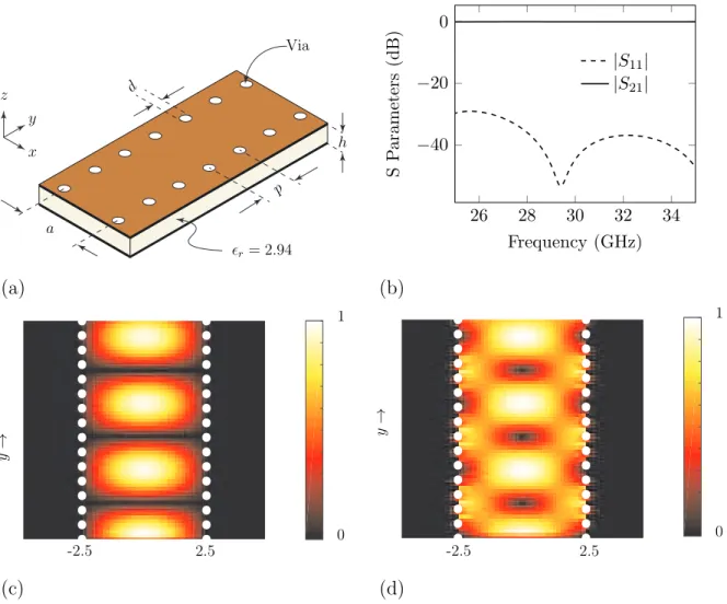
x y z p d a h Via ǫr= 2.94 26 28 30 32 34 −40 −20 0 Frequency (GHz) S P ar am et er s (d B ) |S11| |S21| (a) (b) 1 0 -2.5 2.5 y → 1 0 -2.5 2.5 y → (c) (d)
Figure 2.5: (a) 3D model of an uniform SIW and its dimensions are h = 0.508, d = 0.4,
p = 0.8 and a = 5 (all are in mm); (b) S-parameters of a two-port reciprocal uniform SIW model; (c) Top view of |E| field (V/m) inside uniform SIW, normal toz; and, (d) Top View of |H| field (A/m) inside uniform SIW, normal toz.
copper cladding of thickness 17.5µm on both top and bottom sides of the substrate as shown in figure 2.5(a). The SIW is in the xy plane; the two wave-ports are positioned at the end of the SIW and are normal to the y axis. The simulated scattering parameters for the two-port uniform SIW is given in figure 2.5(a). As seen in figure 2.5(b) most of the energy is transferred from port 1 to 2; which is captured by the|S21|parameter, and is less than -0.12 dB across the frequency range 25 - 35 GHz. The distance between the SIW side walls is such that the waveguide operates in the TE10 dominant mode. The electric and magnetic
field components existing inside the uniform SIW are Ez,Hx, and Hy. The illustration of a
contour plot for both electric and magnetic fields at 30 GHz are shown in figures 2.5(c) and 2.5(d) respectively.
x y z Ls Ws Wc Lcpw ds ǫr= 2.2 h
Top View Bottom View
Figure 2.6: SIW cavity backed planar slot antenna (redrawn from [12]).
2.5
SIW based Slot Antennas
2.5.1 Linearly Polarized Antennas
In [12], a low-cost, low-profile planar slot antenna is constructed on a thin Rogers 5880 dielectric substrate using an SIW cavity as shown in figure 2.6. The thickness of the substrate is ≃ λ0/50 (where λ0 is the free space wavelength at 10 GHz). The SIW cavity is excited by constructing a grounded coplanar waveguide (GCPW), and the cavity dimensions are designed to form TE120 mode. A slot is etched on the opposite side of the GCPW. The
surface currents are maximum and are pointing in the longitudinal direction (along the y -axis). Due to the resonance characteristics of the slot at a single frequency (i.e., at 10 GHz), the impedance bandwidth is found to be 1.7%. The gain and front-to-back ratio (FTBR) are found to be 5.4 dB and 16.1 dB, respectively.
Further, to overcome the narrow impedance bandwidth of the slot antenna [12], two antenna designs are proposed in [13] and [14]. In [13], a bow-tie slot is etched in the place of the narrow slot using the similar concept presented in [12]. Figure 2.7 displays the top and bottom view of the proposed bow-tie slot antenna in [13]. The impedance bandwidth is improved to 9.4% from 1.7% by generating two modes (TE110 and TE120) inside the bow-tie
slot. The resonances of these modes are at frequencies 9.98 GHz and 10.6 GHz. As reported, a minimum gain of 3.53 dB is achieved over the impedance bandwidth and has an FTBR of 15 dB and 20 dB, at 9.98 GHz and 10.6 GHz, respectively.
B x y z h ǫr= 2.2 L lin W Ls Wb Ws
Top View Bottom View
Figure 2.7: SIW cavity backed bow-tie slot antenna (redrawn from [13]).
x y z ǫr= 6.15 Matching post L W h Ls Ws Top View Bottom View
Figure 2.8: SIW cavity backed wide slot antenna (redrawn from [15]).
relative permittivity, ǫr = 6.15 at 60 GHz as shown in figure 2.8. A matching post is
inserted to the substrate close to the radiating element, which acts as a resonant cavity at 62.8 GHz. A slot with width to length ratio (WLR) = 0.71 produces another resonance at 59.2 GHz. Thus, when these two resonances are close to each other, a wideband impedance bandwidth of about 11.6% is achieved from the range 57 - 64 GHz. The simulated gain at resonant frequencies (59.2 GHz and 62.8 GHz) are 7.4 dB and 7.9 dB, respectively. To further increase the gain, a 2×4 antenna array was constructed, as shown in figure 2.9. The impedance bandwidth of the array was 11.5%, and the measured gain was less than 12 dB for the overall bandwidth. In [16], a planar array antenna consisting of 12×12 radiating elements (slots) was excited by designing a 12-way linear power divider as shown in figure 2.10. The frequency of operation for this antenna array was at 60 GHz. The given impedance bandwidth is about 4.12%, and the maximum gain is 22 dB.
x y z
waveguide rectangular (WR) to SIW transition
Figure 2.9: A SIW cavity backed wide slot antenna array consisting of 2×4 elements (redrawn from [12]).
GCPW to SIW transition
Figure 2.10: High gain planar array antenna designed at 60 GHz (redrawn from [16]).
2.5.2 Circularly Polarized Antennas
A compact circularly polarized (CP) antenna is shown in [17]. The antenna is designed using a Rogers 5880 substrate of thickness, h = 0.5 mm ≃ λg/40 (where λg = λ0/√ǫr is
x y ǫr= 2.2 Lc Wc Ls2 Ls1
Top View Bottom View
Figure 2.11: SIW cavity backed crossed slot antenna (redrawn from [17]).
x y z
Elliptical slot (top)
Projection of rectangular slot
Top View Bottom View
Figure 2.12: Wideband circularly polarized SIW cavity-backed antenna (redrawn from [18]).
etched on top of the SIW cavity fed by GCPW. Also, the slots are rotated by 45◦ relative to
one another, as shown in figure 2.11. The CP from the slot is achieved by establishing two orthogonal modes (TE120 and TE210) inside the square SIW cavity. The reported, measured
impedance bandwidth and axial ratio (AR) bandwidth for the antenna are 3% and 0.8%, respectively. The gain varies from 6 - 6.15 dB in the impedance bandwidth, and the FTBR is about 29.6 dB.
Further, a multi-layer antenna configuration consisting of two or more substrates was preferred to achieve CP at 24.5 GHz and 60 GHz. In [18], the short-circuited SIW carrying its dominant (TE10) mode was constructed on a thin bottom layer. A rectangular slot is
etched on top of the SIW close to the short-circuited wall. On top of the rectangular slot, the elliptical cavity using SIW technology is constructed on a thick dielectric substrate. The elliptical cavity is rotated by 45◦ relative to the rectangular slot, and an elliptical slot is
Top View Bottom View Air filled square SIW cavity
on middle layer
Projection of rectangular slot from bottom layer
Figure 2.13: Three layered SIW cavity based CP antenna (redrawn from [19]).
constructed on the top metal layer, as shown in figure 2.12. The observed wide impedance bandwidth is about 42.2%. Due to the combined resonance of the slot and the elliptical cavity. The observed, AR bandwidth is 5.6%, and the gain of the antenna varies from 7.6 -8.7 dB in the impedance bandwidth.
In [19], a longitudinal rectangular slot is constructed on an SIW waveguide to resonate at 60 GHz. Above the slot, a square air-filled SIW cavity is constructed on a thick substrate by removing copper traces on both sides. Above the cavity, a modified circular patch to achieve CP has been etched on a fragile substrate (top layer) as shown in figure 2.13. The AR bandwidth and the impedance bandwidth of the proposed antenna are 6.6% and 11.57%, respectively. The average gain for the impedance bandwidth is 7.8 dBic.
Chapter 3: The Linear and Circular Polarized Cylindrical Sector
(CS)-SIW Narrow Slot Antenna
3.1
Introduction
In general, the slot antenna suffers from narrow bandwidth due to its’ resonant behavior [12]. To increase the slot antenna bandwidth (>9.5%), a bow-tie slot; a cavity slot antenna on a thick (≃ 0.32λg) dielectric substrate [15] is presented. However, in this chapter, we
are proposing a SIW slot antenna on a thin (0.09 λg) substrate which can achieve >10%
bandwidth at the center frequency, fc, 30 GHz.
The methodology for the design of the CS-SIW narrow slot antenna is as follows: the concept and realization of the cylindrical sector SIW from the conventional SIW model. Fur-ther, to excite the CS-SIW model, two transitional layers are constructed using microstrip line and SIW. Later, the slot is etched on the top layer of the CS-SIW. The antenna model is designed and simulated using a commercial 3D EM software, Computer Simulation Tech-nology (CST) (version 2017.05) [20]. Parametric analysis was used in CST to study the dimensions and position of the slot.
Further, to validate the simulated results (such as reflection coefficient, |S11|, gain, and principal plane radiation patterns) obtained from the CST software. A CS-SIW antenna was fabricated and measured. The antenna reflection coefficient was measured using a vector network analyzer (VNA). Both the gain and the radiation patterns are measured using the anechoic chamber. Finally, a comparison is made between the measured and the simulation results.
In addition, in this chapter, we design a three-layer meander-line polarizer unit cell to transform linear to circular polarized waves using CST software. Also, the polarizer and the CS-SIW slot antenna (acting as a source to polarizer) is designed and simulated at around ≃30 GHz. The prototype of both the polarizer and antenna are fabricated and measured. Later, a comparison is made between the simulated and measured results.
x y z h c m b ǫr= 2.94 φ e f g k l a
Figure 3.1: 3D view of CS-SIW narrow slot antenna and its corresponding dimensions (in mm) are: h= 0.508, a= 5, b= 15.78, c= 6, e= 13.6,f = 28.08,g = 19.2,k= 1.31,l = 14,
m= 1.28 and φ = 67◦.
3.2
Proposed LP CS-SIW Narrow Slot Antenna
The 3D model of the proposed linearly polarized (LP) CS-SIW narrow slot antenna is shown in figure 3.1. The designed antenna is along the xy plane referenced by the rectan-gular coordinate system and constructed on a layer of Rogers 6002 substrate with relative permittivity, ǫr = 2.94±0.04, at 10 GHz and loss tangent, tanδ = 0.0012. The height or
thickness of the substrate is, h= 0.508 mm, which is along the +z coordinate.
The antenna design is divided into three sections; namely, microstrip line, SIW, and CS-SIW. These sections are involved in the construction of two transitional layers. The transitional layers are essential at the medium discontinuities to minimize the reflections back to the source (see [9], sec 2.6). For an EM wave, traveling from source to radiating element (i.e., slot): the first encountered transitional layer is from, microstrip line to SIW and the second from, SIW to CS-SIW. At first, we shall begin with the construction of the CS-SIW structure and followed by a discussion on the transitional layer(s).
3.2.1 Cylindrical Sector Substrate Integrated Waveguide (CS-SIW)
b) of the SIW at the other end; such that the width of the SIW is continuously increasing in the transverse plane from a →b along the longitudinal direction (which is also the wave propagating direction). The new resulting model is referred to as cylindrical sector SIW. The term sector corresponds to the area of SIW sidewalls. The term cylindrical is prefixed because the waves traveling inside the sectoral SIW has cylindrical equiphase surfaces (see [21], p.29; [22], p.85). Hence, to define the CS-SIW structure, a cylindrical coordinate system is chosen, since CS-SIW sidewalls are along the direction of radius, r, at an angle, φ, referenced from the origin (r= 0, φ= 0◦, z = 0).
3.2.2 SIW to CS-SIW
We know from section 2.4, SIW structure support only TEm0 above the cut-off frequency.
The SIW is designed to operate in Ka-band (26 - 40 GHz) carrying dominant TE10 mode
only. Thus, when the CS-SIW structure is fed with SIW dominant mode, TE10, the mode
inside the CS-SIW is TE10. However, TE10mode in CS-SIW travel radially (alongr) and the
equiphase surfaces are cylindrical along aφzplane. As the CS-SIW sidewall width increases, higher-order modes (such as TE20) can be excited. Therefore, to restrict the excitation of
higher-order modes, design parameters that control the CS-SIW sidewall, length, and width are chosen carefully. Further, the CS-SIW is terminated with a short circuit load. As a result, standing waves are formed within the CS-SIW. The normalized electric and magnetic field intensity standing wave patterns for the TE10 mode are shown in figures 3.2(a) and
3.2(b), respectively at 30 GHz.
For the standing waves to radiate into free space, a narrow slot was etched on the top metal of the CS-SIW at a distance, k, from the CS-SIW short circuit load. It is indeed complex to calculate the CS-SIW guided wavelength,λg, owing to its’ non-uniform structure.
Therefore, the optimum value for the narrow slots’ position, length, and width were studied by simulating the antenna using CST software in parameter sweep mode.
3.2.3 Microstrip Line to SIW
Numerous options are available to excite an SIW structure, for instance, a coaxial probe, microstrip line, Grounded Co-Planar Waveguide (GCPW). However, the transition from the coaxial probe to SIW (see [9], p.214 - although shown by working with rectangular waveguide) is indeed difficult to realize owing to the non-planar structure. Therefore, planar transitions
0 0.25 0.5 0.75 1 −10 0 10 0 10 20 x(in mm) y (in m m ) 0 0.25 0.5 0.75 1 −10 0 10 0 10 20 x (in mm) y (in m m ) (a) (b)
Figure 3.2: (a) Normalized standing wave pattern of the electric field intensity, |E|, (in V/m) inside CS-SIW at 30 GHz; (b) Normalized standing wave pattern of the magnetic field intensity, |H|, (in A/m) inside CS-SIW at 30 GHz.
such as microstrip line or GCPW are preferred as they can be realized on the same substrate along with the antenna.
In this thesis, we have chosen the microstrip line to excite the SIW owing to its’ simplicity. Consequently, to understand the reflection and transmission properties, a microstrip - SIW - microstrip transition is designed on Rogers 6002 substrate with ǫr = 2.94 at 10 GHz, loss
tangent, tanδ = 0.0012, and thickness, h= 0.508 mm using CST software as shown in figure 3.3(a). The width of the microstrip line is calculated to be, m=1.28 mm for Z0 = 50Ω (using [9], Eqn. 3.196). The SIW is designed to operate at around 30 GHz. The width, via diameter and the via periodicity of the SIW, are a= 5 mm, d = 0.4 mm, and p= 0.8 mm, respectively. Two wave ports are constructed at the cross-section of the microstrip and are,
l, distance apart.
The MS-SIW-MS transition model is simulated using CST software. The transition is symmetry normal to the xz-plane. Thus, simulating [S]-parameter for only one-port would suffice. The width of the microstrip line was tapered from, m tob, to match the impedance between SIW and microstrip line. The simulated reflection and transmission coefficient are found to be< -25 dB and>-0.45 dB, respectively as shown in figure 3.3(b). Therefore, the insertion loss is only 0.225 dB (= 0.45/2) for a one-sided microstrip to SIW transition across
x y z m a d p b l h ǫr= 2.94 26 28 30 32 34 −40 −30 −20 −10 0 Frequency (GHz) S P ar am et er s (d B ) Sim. |S11| Sim. |S12| (a) (b)
Figure 3.3: MS-SIW-MS transition (a) 3D view and its corresponding dimensions (in mm) are a = 5, b= 1.7,d= 0.4, h= 0.508, p= 0.8 andm = 1.28 (b) Plot of two-port scattering parameters (in dB) versus frequency (in GHz).
3.3
Results and Discussion
The fabricated prototype of the LP CS-SIW narrow slot antenna is shown in figure 3.4, and the end-launch connector is used to measure the antenna. The connector has a characteristic impedance, Z0 = 50 Ω. However, for practical applications, the connectors are not required to feed the antenna. The output of the RF component (such as filter, low noise amplifier (LNA) or power amplifier (PA)) is connected with antenna using any methods of the waveguiding structures.
The LP CS-SIW narrow slot antenna model shown in figure 3.1 was also simulated using CST software by designing a waveguide port at the beginning of the microstrip line. The simulated reflection coefficient,|S11|, and the realized gain plots versus frequency are shown in figure 3.5(a). As read from figure 3.5(a), the impedance bandwidth of the antenna is from 28.7 - 32.0 GHz, and the calculated fractional bandwidth is found to be 10.87%. The simulated realized gain varies from 8.33 - 8.84 dB, and the simulated radiation efficiency is above 87.22% throughout the impedance bandwidth. The measured antenna properties for the reflection coefficient, |S11| and the realized gain versus frequency are shown in figure 3.5(b).
Figure 3.4: (Top) The top-view of CS-SIW narrow slot antenna prototype. (Bottom) The CS-SIW narrow slot antenna, antenna under test (AUT), for radiation pattern measurement inside the anechoic chamber.
29 30 31 32 −20 −10 0 10 Frequency (GHz) (V al u e in d B ) Sim. |S11|
Sim. Realized Gain
30 31 32 33 −20 −10 0 10 Frequency (GHz) (V al u e in d B ) Sim. |S11|
Sim. Realized Gain Meas. |S11|
Meas. Realized Gain
(a) (b)
Figure 3.5: LP CS-SIW narrow slot antenna (a) plot of simulated |S11| (in dB) and realized gain (in dB) versus frequency (in GHz) for ǫr = 2.94 ; and, (b) plot of simulated |S11| (in
dB) and realized gain (in dB) versus frequency (in GHz) for ǫr = 2.7.
and the simulated reflection co-efficient, |S11|. The shift in the frequency could be due to the change in relative permittivity, ǫr, of the Rogers 6002 substrate used during fabrication. To
validate this behavior, the ǫr of the Rogers 6002 substrate was varied and simulated using
CST software. Thus, when ǫr= 2.7 (8.5% change), the simulated1 and the measured, |S11|
for the CS-SIW narrow slot antenna are close to each other as shown in figure 3.5(b). The measured realized gain varies from 8.56 - 9.1 dB over the impedance bandwidth.
The complex input impedance (in Ω) of the LP CS-SIW narrow slot antenna versus fre-quency (in GHz) is shown in figure 3.6(a),(b). The plot of normalized electric field intensity, Ey (in V/m), inside the slot versus slot length, l, (in mm) at 30 GHz, 31 GHz, 32 GHz,
and 33 GHz are shown in figure 3.6(c) and finally, the plot of impedance bandwidth (in %) versus slot length, l, (in mm) is shown in figure 3.6(d).
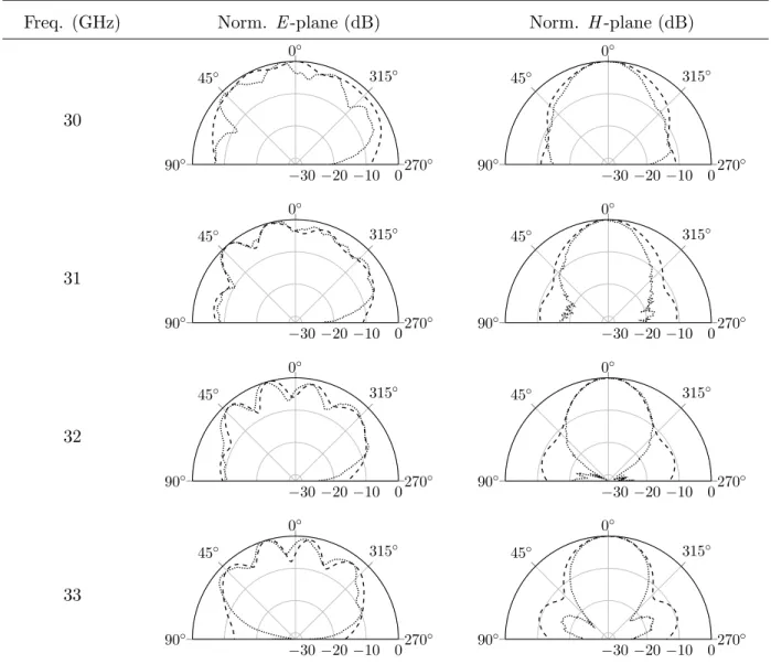
The simulated and measured normalized E-plane and H-plane radiation patterns1 for
the CS-SIW narrow slot antenna at multiple frequencies are shown in figure 3.7.
The ripple effect for the simulated E-plane radiation pattern is less when compared to measured because the simulated antenna using CST was analyzed and excited with waveguide
1
For all the antenna designs discussed in the future chapters; the plot of simulated reflection coefficient, re-alized gain and principal radiation patterns are depicted for Rogers 6002 substrate with relative permittivity,
ǫr= 2.7.
1
A compact range anechoic chamber is used for all the antenna pattern measurements at Polytechnique Montreal University
30 31 32 33 30 45 60 75 Frequency (GHz) R e( Z ) 30 31 32 33 −20 0 20 Frequency (GHz) Im ( Z ) (a) (b) 0 3.5 7 10.5 14 0 0.2 0.4 0.6 0.8 1 Slot Length, l (mm) N or m . Ey (V /m ) 30 GHz 31 GHz 32 GHz 33 GHz 8 10 12 14 0 5 10 15 Slot Length, l (mm) Im p ed an ce Ba n d w id th (% ) (c) (d)
Figure 3.6: (a) and (b) Plot of complex input impedance (in Ω) versus frequency (in GHz), (c) plot of normalized electric field intensity, Ey, (in V/m) inside the slot versus slot length,
l, (in mm) at various frequencies, and (d) plot of impedance bandwidth (in %) versus slot length,l, (in mm).
port (but not with connector). The ripples observed in the measured E-plane radiation pattern are due to the presence of end launch connector (constructed using metal) and localized edge diffraction (see [1], p.730). The size of the connector2 is equal to 10.34 ×8.89
× 8.15 mm3, which is comparable to the λ0 at 30 GHz.
The EM waves emanating from the slot, travel along they-axis (as planar conductor act as a hard surface [23]). The waves then impinge on a connector producing induced currents and the fields are scattered in arbitrary directions, which may sum up either constructively
Freq. (GHz) Norm. E-plane (dB) Norm. H-plane (dB) 30 270◦ 315◦ 0◦ 45◦ 90◦ −30−20−10 0 270 ◦ 315◦ 0◦ 45◦ 90◦ −30−20−10 0 31 270◦ 315◦ 0◦ 45◦ 90◦ −30−20−10 0 270 ◦ 315◦ 0◦ 45◦ 90◦ −30−20−10 0 32 270◦ 315◦ 0◦ 45◦ 90◦ −30−20−10 0 270 ◦ 315◦ 0◦ 45◦ 90◦ −30−20−10 0 33 270◦ 315◦ 0◦ 45◦ 90◦ −30−20−10 0 270 ◦ 315◦ 0◦ 45◦ 90◦ −30−20−10 0
Figure 3.7: Measured (dotted) and simulated (dashed) normalized radiation patterns (E -plane (φ= 90◦) andH-plane (φ= 0◦)) for CS-SIW narrow slot antenna at multiple
frequen-cies.
or destructively with the E-field radiating from the slot. Two methods can be employed to reduce the ripple effect namely: (1) increase the distance between the connector and radiated fields from the slot, and (2) to construct a soft surface on the top layer of the antenna.
However, the ripple effect is not observed for the radiated H-field because the connector andH-field are orthogonal to each other. Thus, simulated and measured normalizedH-plane radiation pattern is not disturbed at all the frequencies, as illustrated in figure 3.7.
3.4
Proposed LP CS-SIW Narrow Slot Antenna for Gain
Improve-ment
A top layer consisting of rectangular copper slabs and an electromagnetic bandgap (EBG) unit cells are constructed using Rogers 3003 ungrounded substrate, to further increase the gain of the LP CS-SIW narrow slot antenna as shown in figure 3.8.
The relative permittivity, ǫr, loss tangent, tanδ and the thickness, c2 of the Rogers 3003
substrate are 3±0.04 at 10 GHz, 0.001 and 0.787 mm, respectively. The top substrate is symmetrical along xz plane, and its’ dimensions are e2×f2. The substrate is placed on top of the CS-SIW slot antenna at a point, P = (e2/2, f2/2). The point, P is also equal to the slot center position. For the EM fields to radiate from the slot, the volume (a2×b2×c2 mm3)
of the Rogers 3003 substrate is hollow. Distance,b2, separates the two rectangular slabs. For each slab, two rows of via are constructed. The length, diameter and the periodicity of the via arec2, 0.4 mm and 0.8 mm, respectively. The via connects the top layer of the slot with the rectangular slab; this whole region acts as a volume made of copper. The dimensions of each copper volume are (d2−b2)/2×a2×c2 mm3.
The analysis for the antenna model shown in figure 3.8 is as follows. The EM fields radiated from the slot travels along the broadside (i.e., +z) direction. These radiated fields produce an induced current when incident on the rectangular slab. Since the radiated H fields from the slot are along x axis, the induced currents on the slab are along y direction (by applying PEC boundary condition). The width of the slab is designed to be a quarter wavelength at the center frequency of antenna operation. The quarter wavelength acts as an open and short circuit load, and the standing waves are formed along y axis. Using image theory for the slab E field distribution, we can replace the slab with a magnetic current. These magnetic currents act as a secondary radiating source and help in increasing the gain of the antenna by adding constructively with the slot’s radiation (which acts as primary radiating source). This technique to increase the gain of the antenna is shown in [24, 25].
3.4.1 Design of EBG Unit Cell
The motivation of designing electromagnetic bandgap (EBG) unit cells on the top layer, is to reduce the ripple effect for the principal E-plane radiation pattern, as observed in figure
x y z a1 b1 c1 d1 φ f1 h1 g1 e1 ǫr= 2.7 c2 d2 a2 b2 e2 f2 g2 ǫr= 3
Figure 3.8: Multilayer CS-SIW narrow slot antenna for improving gain and its corresponding dimensions (in mm) are: a1 = 1.28, b1 = 0.508, c1 = 6, d1 = 14.4, f1 = 1.31, h1 = 14,
g1 = 15.87,e1 = 35.29, c2 = 0.787,d2 = 10.8,a2 = 15.5,b2 = 6, e2 = 24, f2 = 19.2,g2 = 2.4, and φ = 67◦.
conductor (AMC) [26]. An AMC is an engineered structure offering high impedance surface by designing a group of periodic EBG unit cells. These structures are created because the perfect magnetic conductor (PMC) doesn’t exist in nature. However, AMC’s provide a high impedance surface only to a range of frequencies, due to their periodicity.
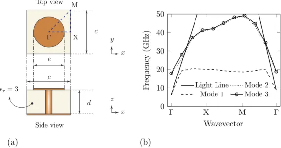
Therefore, designing an AMC surface within the frequency band of interest is crucial. To achieve the bandgap phenomenon (or a high impedance surface) for the overall LP CS-SIW narrow slot antenna impedance bandwidth, an EBG unit cell is modeled and simulated using CST software by eigensolver method as shown in figure 3.9(a). Theperiodic boundary conditions are along the x and y axis, and the PEC (Etan = 0) boundary conditions are at
zmin and zmax of the unit cell. The height of thezmax isλ0 from the circular patch (where λ0
is the free space wavelength at the CS-SIW slot antenna center frequency). The simulated EBG unit cell dispersion diagram is depicted in figure 3.9(b). As read from figure 3.9(b), the designed EBG unit cell act as high impedance surface between 20 - 35 GHz frequencies. The
x x y z Top view Side view c c d e Γ X M ǫr= 3 Γ X M Γ 0 10 20 30 40 50 Wavevector F re q u en cy (G H z)
Light Line Mode 2 Mode 1 Mode 3
(a) (b)
Figure 3.9: (a) Top and Side view of the designed EBG unit cell and its corresponding dimensions (in mm) are c = 2.4, d = 0.787 and e = 2 (b) Dispersion diagram for the designed and simulated EBG unit cell. The band-gap phenomenon is observed from 20 - 35 GHz.
wave vector’s, Γ, X, and M in figure 3.9(b) represent imaginary right angle triangular region on the EBG unit cell. This region is known as irreducible Brillouin zone. Since the EBG unit cell is periodically extending in both x and y axis, the phase variation of the guided waves on the unit cell surface along the x axis is plotted from Γ to X. Similarly, the phase is plotted from X to M for the y axis , and M to Γ for both x and y axis (i.e., the diagonal line).
3.4.2 Results and Discussion
The fabricated prototype of the two-layer CS-SIW narrow slot antenna is shown in figure 3.10, and the measurements were taken for |S11|, gain and radiation patterns by sweeping frequency range for about ±3 GHz at 31 GHz. The top and bottom substrates are glued with a layer of epoxy (ǫr 6= 1).
The antenna model shown in figure 3.8 was designed and simulated with end-launch connector using CST software. The plot of simulated and measured |S11| (in dB) versus frequency (in GHz) is shown in figure 3.11(a). The simulated impedance bandwidth of the antenna is from 30 - 33.3 GHz, and the calculated fractional bandwidth is 10.42%. A
Figure 3.10: (Top) The top-view of the multi-layer CS-SIW narrow slot antenna prototype. (Bottom) The multi-layer CS-SIW narrow slot antenna for radiation pattern measurement inside the anechoic chamber.
30 31 32 33 −20 −10 0 10 Frequency (GHz) (V al u e in d B ) Sim. |S11|
Sim. Realized Gain Meas. |S11|
Meas. Realized Gain
30 31 32 33 0 4 8 12 Frequency (GHz) R ea li ze d G ai n (d B )
Sim. Top Layer Meas. Top Layer Sim. w/o Top Layer Meas. w/o Top Layer
(a) (b)
Figure 3.11: (a) Plot of simulated and measured reflection coefficient, |S11|, (in dB) and realized gain (in dB) versus frequency (in GHz) for the CS-SIW narrow slot antenna gain improvement; and (b) Comparison between simulated and measured realized gain (in dB) versus frequency (in GHz) for with and without top layer.
could be due to the epoxy substance (wasn’t considered during simulation). Both simulated and measured reflection coefficients are around -10 dB, which we find acceptable.
The simulated gain of the antenna is in between 10.5 - 11.44 dB for the overall impedance bandwidth, while, the measured realized gain of the antenna is the range 10.29 - 10.9 dB. The maximum gain for the measured antenna is observed at 32 GHz. The realized gain comparison plots for with and without top layer is as shown in figure 3.11(b). Thus, the presence of the top layer increases the gain of the single-layer CS-SIW narrow slot antenna by 2.1 to 2.7 dB over the impedance bandwidth.
The principal E and H plane normalized radiation patterns for the multi-layer CS-SIW slot antenna are depicted in figure 3.12 at 30, 31, 32, and 33 GHz. The ripple effect is observed for both the simulated and measured principal E plane patterns due to the presence of the connector at a shorter distance to the slot. However, by increasing the distance between the connector and the slot the ripple effect can be further reduced. Consequently, we can also extend the AMC surface to a comparable wavelength along y-axis. The simulated and measured, normalized H plane patterns are similar to each other across frequencies.
Freq. (GHz) Norm. E-plane (dB) Norm. H-plane (dB) 30 270◦ 315◦ 0◦ 45◦ 90◦ −30−20−10 0 270 ◦ 315◦ 0◦ 45◦ 90◦ −30−20−10 0 31 270◦ 315◦ 0◦ 45◦ 90◦ −30−20−10 0 270 ◦ 315◦ 0◦ 45◦ 90◦ −30−20−10 0 32 270◦ 315◦ 0◦ 45◦ 90◦ −30−20−10 0 270 ◦ 315◦ 0◦ 45◦ 90◦ −30−20−10 0 33 270◦ 315◦ 0◦ 45◦ 90◦ −30−20−10 0 270 ◦ 315◦ 0◦ 45◦ 90◦ −30−20−10 0
Figure 3.12: Measured (dotted) and simulated (dashed) normalized radiation patterns (E -plane (φ = 90◦) and H-plane (φ = 0◦)) for CS-SIW slot antenna gain improvement at
multiple frequencies.
3.5
Comparsion With Other mm-wave Antennas
The table 3.1 depicts the comparison between CS-SIW narrow slot antenna (with and without top-layer) with other mm-wave antennas available in the literature. As read from the table 3.1, the proposed CS-SIW slot antenna’s characteristic in terms of both impedance bandwidth and the peak gain are higher when compared with other SIW slot antenna models.
Ref. Freq. (GHz) Impedance Bandwidth (%) Peak Gain (dB) X-pol (dB) Dimension (in λ0) [27] 28 10.2 6.48 30 0.8 × 0.6 × 0.09 [28] 38 15.6 6.5 20 0.7 × 0.9 × 0.06 [12] 10 1.7 5.4 16.1 0.7 × 0.8 × 0.02 [13] 10 9.4 5.4 15 0.9 × 0.6 × 0.03 [15] 60 11.6 7.9 - 2× 0.4 × 0.13 [29] 60 26.4 5.57 - 2.8 × 3.2 × 0.22 [30] 28 8.7 7.5 - 2.8 × 1.9 × 0.07 [31] 28 8.8 12.4 - 1.9 × 1.05 × 0.6 CS-SIW Slot (single layer) 30 10.87 8.84 16 2.8 × 1.6 × 0.05 CS-SIW Slot (multi layer) 30 10.42 11.44 18.2 3.5 × 1.9 × 0.13
![Figure 1.1: Representation of WLAN and WPAN for indoor environment. The coverage area for WLAN is between 10 - 100 m, and WPAN is < 10 m (see [3], fig](https://thumb-us.123doks.com/thumbv2/123dok_us/10129516.2913777/19.918.236.671.100.509/figure-representation-wlan-wpan-indoor-environment-coverage-wlan.webp)

![Figure 2.9: A SIW cavity backed wide slot antenna array consisting of 2×4 elements (redrawn from [12]).](https://thumb-us.123doks.com/thumbv2/123dok_us/10129516.2913777/33.918.215.707.115.401/figure-cavity-backed-antenna-array-consisting-elements-redrawn.webp)