repository: http://orca.cf.ac.uk/105029/
This is the author’s version of a work that was submitted to / accepted for publication.
Citation for final published version:
Balasubramaniam, Senthooran, Ugalde Loo, Carlos, Liang, Jun, Joseph, Tibin, King, R and
Adamczyk, A 2017. Experimental validation of dual H-Bridge current flow controllers for meshed
HVdc grids. IEEE Transactions on Power Delivery 10.1109/TPWRD.2017.2752301 file
Publishers page: http://dx.doi.org/10.1109/TPWRD.2017.2752301
<http://dx.doi.org/10.1109/TPWRD.2017.2752301>
Please note:
Changes made as a result of publishing processes such as copy-editing, formatting and page
numbers may not be reflected in this version. For the definitive version of this publication, please
refer to the published source. You are advised to consult the publisher’s version if you wish to cite
this paper.
This version is being made available in accordance with publisher policies. See
http://orca.cf.ac.uk/policies.html for usage policies. Copyright and moral rights for publications
made available in ORCA are retained by the copyright holders.
Experimental Validation of Dual H-Bridge Current
Flow Controllers for Meshed HVdc Grids
Senthooran Balasubramaniam,
Student Member, IEEE,
Carlos E. Ugalde-Loo,
Member, IEEE,
Jun Liang,
Senior
Member, IEEE,
Tibin Joseph,
Student Member, IEEE,
Rose King,
Member, IEEE,
and Andrzej Adamczyk
Abstract—The current carrying capability of dc lines is limited by their thermal and electric stress limits. Thus, the line current must be maintained within the permissible operational region to protect the lines from damages. In a dense dc grid, control over each line current cannot be achieved without including additional control devices. In this paper a dual H-bridge current flow controller (2B-CFC) is used to manage the dc grid line power flow by providing dc voltage compensation in series with dc lines. A centralized hierarchical control system is proposed to coordinate the operation between multiple CFCs. A novel voltage sharing control scheme is demonstrated. It is shown that such scheme reduces the workload on a single CFC by sharing the required control voltage between multiple CFCs, and, additionally, can be used to avoid control conflicts among active CFCs during communication failure. An experimental platform consisting on a 3-terminal dc grid and small scale 2B-CFC prototypes has been developed to validate the concepts. For completeness, the CFC performance has been analyzed for overload conditions and when no communication exists. Small-scale dc circuit breakers have been developed to study the CFC performance under a pole-to-pole fault.
Keywords—Current flow controller, dc line, dc circuit breaker, H-bridge, multi-terminal hvdc grids, voltage source converter.
I. INTRODUCTION
T
HE breakthrough in the development of solid-state semi-conductor valves in the 1970s has led to the installation of hundreds of point-to-point HVdc links around the globe. HVdc links are suitable for bulk power transmission over long distances due to their lower losses and cost compared to ac links [1]. Particularly, voltage source converter (VSC) based HVdc links have been increasingly adopted due to their decoupled power flow control, black-start capability, control flexibility and reduced footprint [2], [3]. It is desirable to connect additional VSC terminals to existing point-to-point links in a multi-terminal HVdc (MTdc) configuration to maxi-mize power transfer and to achieve an effective power flow management and operational reliability. It is expected that MTdc grids will facilitate a cross-border energy exchange between different countries and will enable reliable power transfer from offshore wind farms [4].In HVdc systems, dc power can be transmitted via overhead lines (OHLs) or cables. Although cables are inherently suitable for underground or sub-sea transmission and pose a reduced visual and environmental impact compared to OHLs, OHLs are attractive owing to their high voltage and high power handling capabilities and lower cost [5], [6]. However, both dc cables and OHLs have intrinsic operational limits over the amount of
S. Balasubramaniam, C.E. Ugalde-Loo, J. Liang and T. Joseph are with Cardiff University, CF24 3AA, Wales, UK (e-mail: {BalasubramaniamS, Ugalde-LooC, LiangJ1, JosephT}@cardiff.ac.uk). R. King and A. Adamczyk are with GE’s Grid Solutions Business, Stafford, ST17 4LX, UK (e-mail: {Rosemary.King, Andrzej.Adamczyk}@ge.com).
power that can be transferred. These limits are determined by thermal and electric stress characteristics [7], [8].
In a very dense MTdc grid, power flow cannot be reg-ulated independently as it is passively determined by the resistance between dc nodes. Since the line current distribution is uncontrolled, some lines may carry excess current while the remaining ones may be under-utilized. System operation beyond thermal and stress limits could damage OHLs and cables and lead to cascaded failure. In a system with high power demand, such a transmission interruption could be very costly. This problem may be relieved through the installation of auxiliary lines, but at the expense of high capital and environmental costs. Moreover, an effective line current control can only be achieved with the inclusion of additional control structures to the system.
Power flow controllers (PFCs) are power electronics based devices capable of providing dc line current control in MTdc grids [9]. Although one way to control dc line current is through the inclusion of a controlled series variable resistor [9], this approach offers a limited controllability and causes high power losses. In recent years, several voltage source-based PFCs have been proposed to eliminate the shortcomings of a resistive-based solution. These devices require an ac connec-tion which can be established through a step-down transformer [10], [11]. Since these PFCs are electrically coupled to the dc side, the voltage difference between the transformer windings and the ground is equal to the rated dc voltage. Therefore, additional insulation is essential to decrease the capacitance between the windings and ground, but this may in turn increase the transformer size and winding resistance. In addition, volt-age source-based PFCs generate significant current harmonics in the valve winding, leading to further power losses. To eliminate these issues, the device has to be powered inside the dc grid [12]–[15]. An inter dc grid powered PFC is referred to as a current flow controller (CFC) [12].
In [12], the concept of a dual H-bridge CFC (2B-CFC) was presented, with its operation and control being further examined in [16]–[19]. An average model and a small signal stability based model of a 2B-CFC have been presented in [18] and [20], respectively. Although a 2B-CFC has been experi-mentally tested in [17], a constant dc voltage source and active loads were used to represent the converters. Therefore, the interaction between the CFC and VSCs was not experimentally verified. To bridge this gap, the operation and control of a 2B-CFC is experimentally validated in this paper using a 3-terminal meshed MTdc test-rig. The CFC operation is analyzed using monopole and bipole configurations. A novel centralized hierarchical control scheme is introduced to coordinate the operation between multiple 2B-CFCs. To the knowledge of the authors, the interaction between multiple CFCs has only been discussed in [21]. Moreover, a new control strategy is
proposed to increase the grid control flexibility during CFC overloading and absence of communications, with the CFC performance being assessed under such conditions. Although the fault performance of a 2B-CFC has been previously studied in [19] through software simulations, such an initial approach has been extended in this paper to experimental studies. Small-scale solid-state dc circuit breakers (DCCBs) have been implemented to assess the device performance under pole-to-pole dc faults, with the interaction between the DCCB and the 2B-CFC during fault conditions being analyzed.
II. DUALH-BRIDGECFC
A 2B-CFC consists of two electrically coupled H-bridges connected in series with dc lines (see Fig. 1, where H-bridges B1andB2are connected with linesL12andL13, respectively). SwitchesQ1 andQ2 are formed by two anti-series connected IGBTs and are placed in parallel withB1andB2, respectively, to avoid interruptions in the grid current flow and thus ensure the safety of the dc grid upon CFC internal failure. In this configuration, the power taken fromL12is equal to the power added toL13, or vice versa.
In the following subsection, the device operation is ex-plained assuming that current flows from terminal T1 to terminalsT2 andT3unless mentioned otherwise.
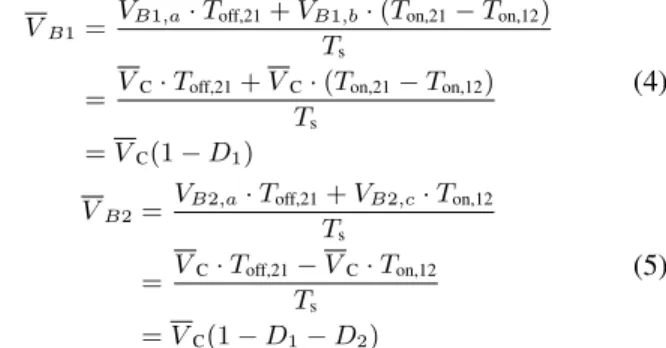
S21 S22 S24 S23 S11 S12 S14 S13 VC iC B1 B2 Q11 Q12 Q1 T2 Q21 Q22 VB2 Q2 T3 i13 T1 i12 i1 L12 L13 VB1 Fig. 1. Topology of a 2B-CFC. A. Operation
The 2B-CFC has the operation modes described below. 1) Zero Compensation (ZC) Mode: In this mode of opera-tion, the required line current reduction or increment is zero and thus the series dc voltage compensation is zero. Therefore, B1andB2must be bypassed. Although this could be achieved by turning on switchesS12andS14ofB1, andS22andS24of B2, the ZC mode is implemented instead by turning switches Q1 andQ2 on (as shown in Fig. 2). The reader is referred to Section V-D for further insight on this.
S21 S22 S24 S23 S11 S12 S14 S13 VC iC B1 B2 Q11 Q12 Q1 T2 Q21 Q22 VB2 Q2 T3 i13 T1 i12 i1 L12 L13 VB1
Fig. 2. Operation under the ZC mode.
2) Current Control (CC) Mode: A required line current reduction or increment is achieved in this mode by providing a negative or positive dc voltage compensation in series to the controlled dc line. The magnitude of the inserted dc voltage is regulated by switching the H-bridge voltage. The active switch on each H-bridge is determined by the control objective and line current directions. If current flows from terminalT1toT2 and from T1 to T3, switches S12 andS21 of B1 andB2 are
modulated to reduce the current on line L12, while all other switches (S11,S13,S14,S22,S23andS24) are maintained off. However, when the current flow is reversed (i.e.fromT2 and T3toT1),S11ofB1andS22ofB2must be modulated instead to reduce the current inL12while the remaining switches (S12, S13,S14,S21,S23andS24) are kept off. For additional insight on the four quadrant switching selection of a 2B-CFC, the reader is referred to [19].
Fig. 3 shows the operational stages of the CFC during the CC mode when current flows from terminal T1 to terminals T2andT3. The switching states of the controlled switches and the corresponding changes on the bridge voltagesVB1andVB2 are shown in Fig. 4. When switchesS12 andS21 are off (Fig. 3(a)), the line currents flow through the naturally commutated diodes and charge the capacitor rapidly. The voltages across terminalsT1 andT2, andT1 andT3, are equal to the inserted dc voltages VB1 andVB2, respectively. These are given as:
VB1,a=VC, VB2,a=VC (1)
where VC is the average value of capacitor voltage VC. This operation results in a decrease in currents i12 andi13.
WhenS21 is on andS12 is off, bridgeB2 is bypassed and B1 charges the dc capacitor (see Fig. 3(b)). In this case,
VB1,b=VC, VB2,b= 0. (2)
As a result of such a positive voltage injection in series with line L12, currenti12decreases whilei13 increases to maintain the power balance.
Conversely, a negative voltage must be inserted in series with L13 to increase line current i13. This can be achieved by switching on both S12andS21 (see Fig. 3(c)). During this period, the capacitor is discharged into L13 and
VB1,c= 0, VB2,c=−VC. (3)
As shown in Fig. 4, continuous switching of S12 and S21 generates a pulsed positive voltage (VB1) across the CFC terminals T1 andT2 and a pulsed negative dc voltage (VB2) across T1 andT3. This increasesi13 and also decreasesi12.
The average bridge voltages VB1 andVB2 can be derived from (1)-(3) as follows:
VB1=
VB1,a·Toff,21+VB1,b·(Ton,21−Ton,12)
Ts
= VC·Toff,21+VC·(Ton,21−Ton,12)
Ts =VC(1−D1) (4) VB2= VB2,a·Toff,21+VB2,c·Ton,12 Ts = VC·Toff,21−VC·Ton,12 Ts =VC(1−D1−D2) (5)
whereD1 is the duty cycle of switchS12,D2 the duty cycle of S21, Ts the switching period, Ton,ab the turn-on time of switch Sab,Tof f,ab the turn-off time of Sab, D1 = Ton,12Ts and D2 = Ton,21
Ts . The relationship between VB1 and VB2 with line currents i12 andi13can be represented by:
PB1 =PB2 VB1·i12=VB2·i13
wherePB1 andPB2are the powers of H-bridgesB1 andB2, respectively. S21 S22 S24 S23 S11 S12 S14 S13 VC iC B1 B2 Q11 Q12 Q1 T2 Q21 Q22 VB2 Q2 T3 i13 T1 i12 i1 L12 L13 VB1 (a) S21 S22 S24 S23 S11 S12 S14 S13 VC iC B1 B2 Q11 Q12 Q1 T2 Q21 Q22 VB2 Q2 T3 i13 T1 i12 i1 L12 L13 VB1 (b) S21 S22 S24 S23 S11 S12 S14 S13 VC iC B1 B2 Q11 Q12 Q1 T2 Q21 Q22 VB2 Q2 T3 i13 T1 i12 i1 L12 L13 VB1 (c)
Fig. 3. Operational stages of a 2B-CFC under the CC mode: (a) Charge mode 1; (b) charge mode 2; (c) discharge mode.
VB1 VB2 t t VC VC -VC VB1 VB2 s T S12 S21 T12,on T21,on
Fig. 4. Switching waveforms for the CC mode.
3) Voltage Control (VC) Mode: Operation under a VC mode is achieved by disabling the line current control loop. This way, the capacitor voltage is regulated regardless of the line current value. To achieve this, the duty cycle of one switch must be set to 1 while the other switch adjusts its duty cycle so that the voltage is maintained constant. For instance, when current flows from terminal T1 to terminalsT2 andT3, the duty cycle of switchS21must be set to 1 while switchS12adjusts its duty cycle. SinceS21is on, the CFC takes only two switching states (see Figs. 3(b) and 3(c)). The VC mode usually takes place under the voltage sharing method presented in Section III. For further information on the detailed operation and control of a 2B-CFC under a VC mode, the reader is referred to [19], where a single modulation strategy is employed to achieve current control by varying the voltage across the capacitor. B. Controller Design
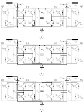
A master-slave (or dual modulation) scheme [19] has been adopted to control a 2B-CFC connected with L12 and L13
(see Fig. 1). The capacitor voltage Vc and line current i13 are controlled independently by modulating switches S12 and S21, respectively. The CFC capacitor voltage control loop is depicted in Fig. 5, where the grey rectangle encompasses the unregulated open loop dynamics. The dynamics of the dc lines are represented by transfer functions Gp1(s)andGp2(s):
Gp1(s) = 1
L12s+R12, Gp2(s) = 1
L13s+R13. (7)
DC terminal voltagesVDC1,VDC2andVDC3are signals which affect the capacitor voltage dynamics in open loop. For control system design, these dc voltages are assumed as disturbances. By applying block diagram reduction techniques, the overall plant transfer functionGv(s)relating the capacitor voltageVC (output) to the duty cycleD1of switchS12(input) is obtained:
Gv(s) =Kc (L12+L13)s+ (R12+R13) L12s+R12 · · 1 L13Cs2+ R13Cs+ 1 (8)
A controller Gk(s)is proposed to ensure an adequate closed-loop performance: Gk(s) =K s+zc s+pc s+zp s (9) Controller Gk(s) in (9) consists of a proportional-integral (PI) structure cascaded with a lead compensator, where zp is the zero of the PI controller, zc andpc are the zero and pole of the lead compensator, and K is the overall controller gain. Such a control structure, if designed properly, is sufficient to provide high stability margins, eliminate the steady-state error and reject disturbances.
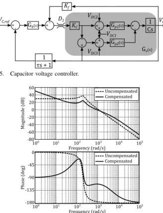
Let the parameters inGp1(s),Gp2(s), andGv(s)be defined as in Tables I and II. Fig. 6 shows the open loop frequency response of Gv(s). The bandwidth of the uncompensated system is 1000 rad/s and this value is kept when Gk(s) is used. It can be also observed in Fig. 6 that the uncompensated system exhibits a poor phase margin (≈ 4 deg). While the PI controller is used to achieve a zero steady-state error, the lead compensator significantly improves the phase margin to ≈ 68 deg to ensure a good performance during transients and solid-state switching (or quadrant selection). Additionally, the CFC capacitor voltage loop considers a feedback loop with a proportional gain Kf to limit the initial overshoot in the capacitor voltage (see Fig. 5). Since the initial voltage across the capacitor is zero, the capacitor voltage controller would adjust the initial duty cycle of the controlled switch to zero. However, since line current flows through the capacitor, this is rapidly charged, which could lead to an overvoltage across its terminals. The feedback compensation provided by proportional gain Kf limits the initial overshoot by moving the duty cycle of the controlled switch towards unity.
Fig. 7 shows the line current control loop. Since plant Gi(s) is a first order function, a PI controller is used. It should be highlighted that a first order filter with a cut-off frequency of200 Hz has been employed with the voltage and current controllers to eliminate measurement noise. The control parameters can be found in the Appendix.
+ -VC,ref + -Kf VC Gk(s) KC Gv(s) +-+ Gp1(s) VDC2 VDC1 +-+ VDC3 -+ 1 Cs Gp2(s) 1 τs+1 D1
Fig. 5. Capacitor voltage controller.
Frequency (rad/s) 100 101 102 103 104 105 0 60 40 20 -20 -40 -60 -80 Magnitude (dB) Uncompensated Compensated Phase (deg) 0 -45 -90 -135 -180 Frequency (rad/s) 100 101 102 103 104 105 Uncompensated Compensated
Fig. 6. System open loop frequency response (Bode plot): Uncompensated systemGv(s)and compensated systemGk(s)Gv(s).
+ -i13,ref i13 1 s + 1 PI KC + -+ Gp2(s) VDC1 VDC3 VB2 Gi(s) D2
Fig. 7. Line current controller.
III. COORDINATED CONTROL OF MULTIPLECFCS
In a complex dc grid, flexible current regulation cannot be achieved with a single CFC. This shortcoming can be relieved by installing CFCs at different locations. Under such a scenario, a centralized control scheme is essential to coor-dinate the operation among the devices. Fig. 8 illustrates the hierarchical control system when multiple CFCs are employed in a meshed-connected MTdc system. The control system consists of a centralized remote control centre (RCC) along with multiple local controllers (LCs). Each CFC is assigned to an LC. The RCC monitors the grid power flow and calculates the required voltage and current reference values prior to scheduled power changes, energy trade or system maintenance (for instance, involving the disconnection of a dc cable). By employing a Broyden-based power flow algorithm [22], [23], the CFC with the minimum capacitor voltage will be assigned to control the line current since a small capacitor voltage implies lower power losses due to smaller ripple.
The LCs include the following control layers: system con-trol, application concon-trol, CFC control and firing control. The system control layer establishes a secure bi-directional data transmission link with the RCC. In addition, it monitors the
Remote Control Centre (RCC) LC 1 CFC 1 CFC Status References DAQ Control LC 2 CFC 2 LC n CFC n
Fig. 8. CFC hierarchical control.
status of each control layer and sends this information back to the RCC. The application control layer accepts the voltage and current reference values set by the RCC and passes the reference values to the CFC control layer through a set of limiters. The CFC control layer is implemented as an array of PI controllers and control blocks. It provides the duty cycle to the firing control layer by processing the references and local measurements. The firing control layer generates the firing pulses to the individual semi-conductor valves.
A. Voltage Sharing - CFC Overloading
The operational range of a CFC can be maximized by increasing the capacitor voltage level. However, such an ap-proach could in turn increase the device footprint and cost. This issue can be overcome by sharing the required dc voltage between multiple CFCs. - + i j Lij -+ Lik k Lkj VB1 VB2 m.VQ2 (a) - + i j Lij -+ Lik k Lkj n.VB1 n.VB2 - + m.VB1 -+m.V B2 (b) Fig. 9. Voltage sharing: (a) Single CFC; (b) Multiple CFCs.
Fig. 9 shows an upgraded dc network with a single CFC and with two CFCs. If a single CFC is used (Fig. 9(a)), dc voltages VB1 andVB2 are required in series with lines Lij andLikto achieve the desired current on lineLij. LetVB1> VC,max, where VC,max is the maximum voltage allowed across the CFC capacitor. For this scenario, the required line current reduction or increment cannot be achieved. However, when two CFCs are included into the dc network (Fig. 9(b)), the required capacitor voltage can be shared between the CFCs in an n :m ratio. The relationships between the required series dc voltages and the capacitor voltage are given by:
n(VB1+VB2)≤VC,max, m(VB1+VB2)≤VC,max, (10) wheren≤1 andm≤1, withn+m= 1.
When more than one CFC is deployed in a common dc line, the control objectives must be established carefully to avoid potential conflicts. Only a single CFC in CC mode is permitted at any given load condition; however, operation of multiple CFCs in VC mode is allowed.
B. Voltage Sharing - Communication Failure
In HVdc systems, fibre optic and power line communication are widely employed for data acquisition and to dispatch control signals. As a result of technological advancements, these communication modalities have become faster and more reliable in recent years. However, a dc grid cannot just rely
on wired-based communication links as they are vulnerable to natural disasters and human errors.
Fig. 10. Offline voltage and current reference calculation.
An MTdc grid should remain operational in case of any communication failure. Although the RCC sets the references for each CFC (and their status), the LCs should be designed to detect overloading conditions and to trigger the CFCs accordingly when communication is lost. In this case, local measurements should be employed. As highlighted previously, preassigned control objectives (i.e., modes of operation) must be established carefully among the active CFCs – with a single CFC acting in CC mode only. Current and voltage references are calculated offline using look-up tables, as shown in Fig. 10, where the dc line currents are used as inputs. For instance, if two CFCs are used, the CFC in a VC mode contributes half of the required capacitor voltage while the other half is approximately provided by CFC in CC mode.
IV. MTDCCONTROL ANDCONFIGURATION
The 3-terminal meshed MTDc grid shown in Fig. 11 is used to validate the operation and control of 2B-CFCs. The VSC terminals have been arranged in a symmetrical monopole configuration and rated at ±125 V and 2 kW. To establish a bipole operation, CFC modules A and B are installed in series with both the positive and negative poles of linesL12andL13. A master-slave control scheme for VSCs has been adopted to maintain the grid power balance [4]. It uses a classical dq reference frame scheme to regulate the dc voltage or active and reactive power.
L12+ B1 B2 L 12-a b c Lg1 VSC 1 Grid 1 L13+ L13- L23+ L 23-a b c Lg3 VSC 3 Grid 3 a b c Lg2 VSC 2 Grid 2 CFC A CFC B i12,+ i 12,-i23,+ i13,+ VDC1 i 13,-i 23,-VDC3 VDC2 B1 B2
Fig. 11. Three-terminal MTdc grid with embedded CFCs.
CFCModules A&B DCNetwork VSC1,2&3 dSPACE dSPACE Controldesk Tr1,2&3
Fig. 12. Experimental setup.
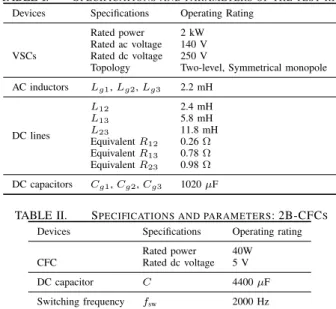
TABLE I. SPECIFICATIONS AND PARAMETERS OF THE TEST-RIG Devices Specifications Operating Rating
VSCs
Rated power 2 kW Rated ac voltage 140 V Rated dc voltage 250 V
Topology Two-level, Symmetrical monopole AC inductors Lg1,Lg2,Lg3 2.2 mH DC lines L12 2.4 mH L13 5.8 mH L23 11.8 mH EquivalentR12 0.26Ω EquivalentR13 0.78Ω EquivalentR23 0.98Ω DC capacitors Cg1,Cg2,Cg3 1020µF
TABLE II. SPECIFICATIONS AND PARAMETERS: 2B-CFCS Devices Specifications Operating rating
CFC
Rated power 40W Rated dc voltage 5 V
DC capacitor C 4400µF
Switching frequency fsw 2000 Hz
Fig. 12 shows the experimental setup of the MTdc test-rig with embedded 2B-CFC prototypes. Each VSC is connected to an ac system through a phase reactor and a transformer. Auto-transformers connected to the415V ac power supply represent the ac grids. A dSPACE DS1005 system is used to control the test-rig. Simulink-based real-time interface control blocks are used to implement the control scheme. Real-time operation is enabled through the ControlDesk 3.2 graphical user interface. For completeness, the specifications and parameters for the test-rig and the 2B-CFCs are provided in Tables I and II.
V. SIMULATION ANDEXPERIMENTALVALIDATION
The results reported in this section have been expressed in per unit considering the following power, voltage and current bases: 2 kW, 125 V, and 8 A. VSCs 1 and 3 are initially set to inject 0.8 and 0.2 p.u. into the MTdc grid, whereas VSC 2 has been designated as a slack busbar that maintains the grid power balance (i.e., maintains a constant dc voltage). A. Transition to CC Mode During System Transients
A test to assess the performance of 2B-CFCs following ramp changes in power is carried out both through a simu-lation and with the experiment platform. To this end, the 3-terminal dc grid equipped with CFCs has been modeled in Simulink/SimPowerSystems. The CFCs are placed at the pos-itive and negative poles of linesL12andL13. CFC operation is coordinated using an RCC and each CFC is equipped with an LC. The RCC determines the state of each CFC by calculating the required CFC capacitor voltage to maintain the line current at a desired value.
In general, a CFC is used to maintain the line current of a given line at or below 1 p.u. However, it should be highlighted that in scaled systems such as in the experimental test-rig in Fig. 12, the forward voltage drop on the semiconductor switches affects the current flow between electrical nodes. During the capacitor charging mode of the CC mode, a maximum of two diodes, each with a forward voltage drop between 0.8 −1 V, are inserted into the conduction path. The capacitor voltage required to achieve an optimum line current distribution may be very small and of a magnitude
similar to the diode’s forward voltage drop. Therefore, to build enough voltage across the capacitor and to demonstrate the CFC performance, a large current reduction must be achieved. In this case the current reference is set to 0.5 p.u., but this value may be just below 1 p.u. in a real system. It must be emphasized that the RCC could be used to determine the optimal CFC current references to achieve the best line current distribution in complex dc grids so that grid power losses are minimized [24].
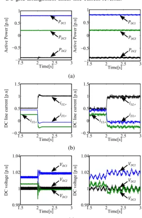
The simulation (left) and experimental results (right) are shown in Figs. 13 to 15. Initially, both CFCs operate in a ZC mode, with switches Q1 andQ2 being turned on. Att= 2s, the power reference of VSC 1 is ramped up from 0.8 to 1.4 p.u. (see Fig. 13(a)). As it can be observed in Figs. 13(b) and 13(c), line currents i12+ and i12− surpass the maximum thermal current limit (of 1 p.u.). Following the overload detection, the LCs are activated to decrease the currents to 0.5 p.u. to achieve a better line current distribution. As a result, the terminal voltages of the converters have increased further to maintain the grid power balance (Fig. 13(d)). It can be observed both in simulation and experimental results that the terminal voltage of the master converter (VDC2) deviates from its reference value to prevent the VSCs from entering into over-modulation.
It can be noticed that a small mismatch in the line current distribution occurs when comparing simulation and experimen-tal results. This is due to forward voltage drops in diodes and converter power losses in the experimental platform. In the simulation, the voltage drops have been fixed to 0.8 V, with converter switching losses being neglected. Therefore, more power is injected into the dc grid in the simulation, which results in a different line current distribution compared to that in the experiment. Since the same current reference is employed for both cases, the required series dc voltage compensation is slightly higher in the simulation given that an additional current reduction is required.
Figs. 14 and 15 provide the voltage profiles of the CFCs. For the experiment, the capacitor voltages are maintained at 0.035 p.u., as shown by Figs. 14(a)and 15(a). Such voltage value is determined by the RCC. However, the required capacitor voltage is 0.004 p.u. higher for the simulation as a result of the grid’s initial current distribution and voltage profile (the RCC uses instantaneous grid measurements to determine the capacitor voltage). During the CC mode, mean dc voltages VB1andVB2are inserted in series with linesL12+andL13+, respectively. This is shown in Fig. 14(b). Since the line current flows in an opposite direction, the signs of the inserted dc voltages in series with L12− and L13− (see Fig. 15(b)) are opposite with respect to those shown in Fig. 14(b). In the ZC mode, fixed dc voltages are observed across bypass switches Q1 andQ2 due the forward voltage drop of the diodes.
In this test case, the results have shown that a CFC can be used to protect a dc line during line overloading by con-trolling the line current below its thermal limit. Additionally, a CFC could be employed to reduce the amount of wind power curtailment through the rescheduling of grid power flow [24]. Another application of a CFC is to interrupt current on a specific dc line to facilitate its maintenance without interrupting the dc grid operation. Although it is expected that a CFC would incur some power losses, its benefits outweigh
1.5 2 2.5 3 1.5 1 0.5 0 0.5 1 1.5 Time[s]
Active Power [p.u]
PDC1 PDC2 P DC3 1.5 2 2.5 3 1.5 1 0.5 0 0.5 1 1.5 Time[s]
Active Power [p.u]
PDC1 PDC2 PDC3 (a) 1.5 2 2.5 3 0.25 0 0.5 1 1.25 Time[s]
DC line current [p.u]
i12,+ i23,+ i13,+ Time[s] 1.5 2 2.5 3 0.25 0 0.5 1 1.25
DC line current [p.u]
i12,+ i23,+ i13,+ (b) 1.5 2 2.5 3 0.25 0 0.5 1 1.25 Time[s]
DC line current [p.u]
i 12,-i 23,-i 13,-1.5 2 2.5 3 0.25 0 0.5 1 1.25 1.25 Time[s]
DC line current [p.u]
i 12,-i 23,-i 13,-(c) DC voltage [p.u] 1.5 2 2.5 3 0.98 1 1.02 1.04 1.06 Time[s] VDC1 V DC2 VDC3 1.5 2 2.5 3 0.98 1 1.02 1.04 1.06 Time[s] DC voltage [p.u] VDC1 VDC2 VDC3 (d)
Fig. 13. DC grid response for a ramp change in power. Simulation (left) and experimental (right) results: (a) VSC active power; (b) dc line current (positive pole); (c) dc line current (negative pole); (d) dc terminal voltage.
this shortcoming as the device can serve multiple purposes. It could be argued that the use of CFCs in dc grids may be economically feasible; however, an economic feasibility analysis is out of the scope of this paper and requires further investigation.
B. Coordinated Operation of Multiple CFCs
In this experiment, the coordination between two 2B-CFCs is examined when no communication between the LCs and the RCC exists. Fig. 16 depicts the system configuration for this test. CFC A is installed between the positive poles of lines L12andL13, whereas CFC B is installed between the positive poles ofL13andL23. The voltage sharing method described in Section III is adopted to provide the required current control. Both CFCs are initially operated in a ZC mode. At t = 2 s, the power reference of VSC 1 is ramped up from 0.8 to 1.4 p.u. Since there is no communication between the CFCs and the RCC, the LCs determine the reference set-points and dictate the CFC control following the detection of an overload condition. CFC A is set to operate under a CC mode while
(a) 1.5 2 2.5 3 0.04 0.02 0 0.02 0.04 0.06 Time[s] VB1 & V B2 [p.u] 1.5 2 2.5 3 0.04 0.02 0 0.02 0.04 0.06 Time[s] VB1 & V B2 [p.u] VB1 VB2 VB1 VB2 (b)
Fig. 14. Response of the CFC located at the positive pole for a ramp change in power. Simulation (left) and experimental (right) results: (a) capacitor voltage; (b) inserted mean dc voltages.
1.5 2 2.5 3 0 0.02 0.04 0.06 Time[s] VC [p.u] 1.50 2 2.5 3 0.02 0.04 0.06 Time[s] VC [p.u] (a) 1.5 2 2.5 3 0.06 0.04 0.02 0 0.02 0.04 Time[s] VB1 & V B2 [p.u] 1.5 2 2.5 3 0.06 0.04 0.02 0 0.02 0.04 Time[s] VB1 & V B2 [p.u] VB2 VB1 VB2 V B1 (b)
Fig. 15. Response of the CFC located at the negative pole for a ramp change in power. Simulation (left) and experimental (right) results: (a) capacitor voltage; (b) inserted mean dc voltages.
L12+ L 12-L13+ L13- L23+ L 23-B1 B2 B1 B2 CFC A CFC B
Fig. 16. DC grid with two CFCs.
CFC B operates under a VC mode. In CFC B, switches S11 and S22 are modulated during the VC mode as the current flows from T2 toT1 andT3 andT1. As discussed in Section II, the duty cycle of switch S22 is set to 1 and switchS11 is controlled to build up the capacitor voltage.
Fig. 17 shows the dc grid response. Following the change
in set-point power (see Fig. 17(a)), L12+ and L12− become overloaded. This is illustrated in Figs. 17(b) and 17(c). Once this condition is detected, CFC B is enabled to provide half of the required voltage compensation (0.016 p.u.). CFC A is enabled att= 4s to decreasei12+to 0.5 p.u. so that a better current distribution is achieved. It should be emphasized that since no CFC is placed on the negative pole, L12− remains overloaded. The voltage profiles of the CFCs are shown in Figs. 18 and 19. It should be recalled that two diodes are inserted in series with the capacitor during a charging mode (see Fig. 3(b)). In this case, a voltage drop of 0.0065 p.u. (0.8 V) is observed across each diode. As a result, the inserted mean bridge voltagesVB1of CFCs A (Fig. 18(b)) and B (Fig. 19(b)) are higher than their capacitor voltages. The voltage across each capacitor is nearly the same as the CFCs share the required voltage in a 1:1 ratio (see Figs. 18(a) and 19(a)).
0 1 2 3 4 5 1.5 1 0.5 0 0.5 1 1.5 Time[s]
Active Power [p.u]
PDC1 PDC2 PDC3 (a) 0 1 2 3 4 5 0.5 0 0.5 1 1.5 Time[s]
DC line current [p.u]
i12,+ i23,+ i13,+ (b) 0 1 2 3 4 5 0.5 0 0.5 1 1.5 Time[s]
DC line current [p.u]
i 12,-i 23,-i 13,-(c) 0 1 2 3 4 5 0.98 1 1.02 1.04 1.06 1.08 Time[s] DC voltage [p.u] VDC1 VDC2 VDC3 (d)
Fig. 17. DC grid response: (a) VSC active power; (b) dc line current (positive pole); (c) dc line current (negative pole); (d) dc terminal voltage.
It should be highlighted that the experiment presented in this section is an example which demonstrates the need to install a CFC in the positive and negative poles.
C. Line Current Reversal
0 1 2 3 4 5 0 0.01 0.02 0.03 Time[s] VC [p.u] (a) 0 1 2 3 4 5 0.01 0 0.01 0.02 0.03 Time[s] VB1 & V B2 [p.u] VB2 VB1 (b)
Fig. 18. CFC A response: (a) capacitor voltage; (b) inserted mean dc voltages.
0 1 2 3 4 5 0 0.01 0.02 0.03 Time[s] VC [p.u] (a) 0 1 2 3 4 5 0.03 0.02 0.01 0 0.01 Time[s] VB1 & V B2 [p.u] VB2 VB1 (b)
Fig. 19. CFC B response: (a) capacitor voltage; (b) inserted mean dc voltages.
flow in a dc line. Fig. 20 shows the test circuit arrangement, where the CFC is installed between the positive poles of lines L12andL13. Fig. 21 shows the dc grid response. Initially, the CFC is in CC mode and line currenti13+is regulated at 0.25 p.u. During this period, switchesS12andS21are modulated to provide independent capacitor voltage and line current control. Att= 2s, the CFC is requested to reverse the current on line L13+ from 0.25 to -0.25 p.u. Since the active switch on each H-bridge is determined by the control objective and line current directions, switches S13 andS22 are modulated following the current reversal.
Fig. 22 shows the CFC dynamics. The capacitor voltage is regulated at 0.04 p.u. (see Fig. 22(a)). As shown in Fig. 22(b), an average dc voltage VB1 is inserted in series with line L12+ and a voltageVB2 with L13+. Since initially the line currents are in the same direction, VB1 and VB2 have opposite polarities to maintain the power balance between bridges. A positive voltage must be inserted in series with L13+ to decrease the current flow. Following the reversal of i13+, currents i12+ and i23+ now flow in opposite directions and, thus, VB1 and VB2 have the same polarity to maintain the power balance between the bridges.
It should be emphasized that for this example the main objective is to reverse the current flow in a dc line. Therefore,
although this may not be acceptable in practice, changes on other line currents are not warranted further discussion.
L12+ L 12-L13+ L13- L23+ L 23-B1 B2
Fig. 20. DC grid arrangement under line current reversal.
1.51 2 2.5 3 0.5 0 0.5 1 Time[s]
Active Power [p.u]
PDC1 PDC2 PDC3 1.51 2 2.5 3 0.5 0 0.5 1 Time[s]
Active Power [p.u]
PDC1 PDC2 P DC3 (a) 1.5 2 2.5 3 0.5 0 0.5 1 1.5 Time[s]
DC line current [p.u]
1.5 2 2.5 3 0.5 0 0.5 1 1.5 Time[s]
DC line current [p.u]
i12,+ i23,+ i13,+ i12,+ i23,+ i13,+ (b) 1.5 2 2.5 3 0.98 1 1.02 1.04 Time[s] DC voltage [p.u] 1.5 2 2.5 3 0.98 1 1.02 1.04 Time[s] DC voltage [p.u] VDC1 VDC2 VDC3 V DC1 VDC2 VDC3 (c)
Fig. 21. DC grid response during line current reversal: (a) VSC active power; (b) dc line current (positive pole); (c) dc terminal voltage.
D. DC Fault Performance
In MTdc grids, dc faults could lead to large transient currents due to the low dc side impedance. Therefore, the performance of a CFC under dc faults must be assessed to adequately protect the device. CFC protection is mainly determined by the fault current magnitude and the response time of bypass switches. In line with this, an experiment is carried out to evaluate the performance of a 2B-CFC under a pole-to-pole fault. As shown in Fig. 23, the fault is applied between the positive and negative poles of line L12. Small-scale solid-state based DCCBs (as shown in Fig. 24) are installed at each end to interrupt the fault current. MOVs are connected across the bypass switches and the CFC capacitor to protect the device against overvoltages.
Among the DCCBs proposed in the literature, hybrid DC-CBs exhibit high efficiency and an acceptable interruption
1.5 2 2.5 3 0.02 0.03 0.04 0.05 0.06 Time[s] VC [p.u] 1.5 2 2.5 3 0.02 0.03 0.04 0.05 0.06 Time[s] VC [p.u] (a) 1.5 2 2.5 3 0.02 0 0.02 0.04 0.06 Time[s] VB1 & V B2 [p.u] 1.5 2 2.5 3 0.02 0 0.02 0.04 0.06 Time[s] VB1 & V B2 [p.u] VB1 VB2 VB1 VB2 (b)
Fig. 22. CFC response during line current reversal: (a) capacitor voltage; (b) inserted mean dc voltages.
time. With these devices, the losses during the normal opera-tion are minimized through the use of an ultra-fast disconnector and a load commutating switch [25], [26] . However, for the experiment conducted in this section, solid-state DCCBs have been adopted due to their simplicity. Given that the main objective of the experiment is to study the performance of a 2B-CFC under a dc fault, solid-state DCCBs serve the purpose in spite of their power losses. It should be noted that a response time of 5 ms has been used to emulate that of a hybrid DCCB. A communication-less single-ended protection strategy is used to detect the fault. The DCCBs and bypass switches are set to open and close, respectively, if the rate of change in line current is>800p.u./s and the current magnitude is above 1.3 p.u. In addition, if the voltage across the CFC capacitor is 30% above the rated value, the CFC will be switched to a bypass mode to protect it against overvoltage. The system states during the fault are provided in Table III.
L12+ L 12-L13+ L13- L23+ L 23-CB1 CB3 CB2 CB4 B1 B2
Fig. 23. Pole-to-pole fault location.
Energy Absorption Branch
Fig. 24. Schematic of a solid-state DCCB
Fig. 25 shows the fault current through the CFC. During pre-fault conditions, the CFC is set to control line currenti13at 0.5 p.u. and capacitor voltageVCat 0.04 p.u. (5 V). After the fault is applied at t=t0, the magnitude of line currenti12 rapidly increases and i13 decreases, while the CFC capacitor voltage and bridge voltages increase (Fig. 26). This occurs as the CFC
TABLE III. SYSTEM STATE DURING DC FAULT
Time System state
t0 Pole-to-pole fault applied t1 Fault detected by CFC, bypass switches
activated and control signals disabled
t2 Opening of DCCBs
tries to maintain the line current at the reference value since the fault has not been detected yet. Att=t1, the fault is detected by the local protection system and the CFC transitions from a CC to ZC mode. The capacitor voltage remains constant as the H-bridges are bypassed. Fig. 27 shows the voltage profiles of the DCCBs. The fault current is interrupted at t =t2 by opening the DCCBs. As it can be observed, the voltage across each DCCB is equal to the pole voltage.
1.9 1.95 2 2.05 2.1 0.5 0 0.5 1 1.5 2 Time[s]
DC line current [p.u]
t0t2
i12,+
i13,+
Fig. 25. Fault current through CFC
VB2
VB1
VC
t0 t1 t2
Fig. 26. CFC voltage profile
CB1
CB2
CB4 CB3
t0 t1 t2
Fig. 27. DCCBs voltage profile
The results presented in this section have clearly shown that the protection of the 2B-CFC is mainly determined by the response time of the bypass switches Q1 and Q2 and of the DCCBs. A CFC is expected to act independently of a DCCB during a fault as no communication between them exists. In the presence of a slow DCCB, the bypass switches should have a high current rating.
It should be highlighted that a CFC can be operated in ZC mode by activating the switches of the H-bridges, but instead such an operation is implemented using external bypass switches (see Section II-A-2). Although at first glance it could seem that the use of the additional switches is redundant, these
are essential to ensure the correct operation of the dc grid and to protect CFC modules. Given that a CFC is a series-connected device, it should be adequately protected during fault conditions. Therefore, instead of subjecting the H-bridges of the CFC to full dc fault currents until fault clearance, additional parallel branches with bypass switches are used instead to carry the fault current. Additionally, in the event of an internal CFC failure, the device must be bypassed to avoid any interruption to the line current flow and this is easily done with the additional switches.
VI. CONCLUSIONS
In this paper, the operation and control of 2B-CFCs have been experimentally validated in a meshed MTdc grid test-rig against simulation results. The results demonstrate that a CFC can be used to improve the grid reliability by limiting the line currents below thermal limits. A good agreement has been observed between the experimental and simulation results.
A control scheme has been proposed to achieve an effective transition from the ZC to the CC mode. Additionally, a centralized hierarchical control scheme has been presented to coordinate the operation between multiple CFCs in the MTdc grid. It has been shown that when multiple CFCs are employed, the workload of a CFC that has reached its maximum operating point can be reduced by sharing the dc voltage compensation among the other CFCs. Potential control conflicts between active CFCs can be eliminated by restricting the operation of a single CFC in CC mode and the remaining CFCs in VC mode. For completeness, the performance of the 2B-CFC has been studied under the presence of a pole-to-pole dc fault. It has been observed that a fast protection system is required to protect the device against overvoltages and overcurrents.
APPENDIX
The PI controllers are represented in the form:K(s) =Kp+Ki/s.
Two-level VSCs: Current:Kp= 45,Ki= 45000. DC voltage:Kp= 0.2, Ki= 20. Active power:Kp= 0.2,Ki= 20. Reactive power:Kp= 0.3, Ki= 10.2B-CFC: DC line current:Kp= 12×10−3,K i= 1.2. Capacitor voltage:Gk(s) = 14 5×10⁻³s+ 1 2.1×10⁻⁴s+ 1 13×10−3s+ 1 s
CFC Gain:Kc= 5000. Feedback compensation loop gain:Kf= 0.09.
REFERENCES
[1] N. Flourentzou, V. G. Agelidis and G. D. Demetriades, ”VSC-Based HVDC Power Transmission Systems: An Overview,” IEEE Trans. Power Electron., vol. 24, no. 3, pp. 592-602, March 2009.
[2] D. Jovcic and K. Ahmed,High-Voltage Direct-Current Transmission: Converters, Systems and DC Grids. UK: Wiley, 2015.
[3] D. van Hertem, O. Gomis-Bellmunt, and J. Liang (eds.),HVDC Grids: For Offshore and Supergrid of the Future. USA: Wiley, 2016. [4] J. Liang, et al., ”Operation and Control of Multiterminal HVDC
Transmission for Offshore Wind Farms,”IEEE Trans. Power Del., vol. 26, no. 4, pp. 2596-2604, Oct. 2011.
[5] H. Wang, et al., ”Research on Overvoltage for XLPE Cable in a Modular Multilevel Converter HVDC Transmission System,” IEEE Trans. Power Del., vol. 31, no. 2, pp. 683-692, April 2016.
[6] P. Buijs, D. Bekaert, S. Cole, D. van Hertem, R. Belmans, Transmission investment problems in Europe: Going beyond standard solutions,
Energy Policy, vol. 39, no. 3, pp. 1794-1801, March 2011.
[7] Z. Y. Huang, et al., ”Thermal-Electric Rating Method for Mass-Impregnated Paper-Insulated HVDC Cable Circuits,” IEEE Trans. Power Del., vol. 30, no. 1, pp. 437-444, Feb. 2015.
[8] C. C. Reddy, ”Theoretical Maximum Limits on Power-Handling Ca-pacity of HVDC Cables,”IEEE Trans. Power Del., vol. 24, no. 3, pp. 980-987, July 2009.
[9] Q. Mu, J. Liang, Y. Li, X. Zhou, ”Power flow control devices in DC grids,” inIEEE PES General Meeting, San Diego, USA, pp. 1-7, 2012. [10] E. Veilleux and B. T. Ooi, ”Multiterminal HVDC With Thyristor Power-Flow Controller,”IEEE Trans. Power Del., vol. 27, no. 3, pp. 1205-1212, July 2012.
[11] S. Balasubramaniam, J. Liang and C. E. Ugalde-Loo, ”An IGBT based series power flow controller for multi-terminal HVDC transmission,” in IEEE 49th Intl. Univ. Power Eng. Conf. (UPEC), Cluj-Napoca, Romania, pp. 1-6, 2014.
[12] C. D. Barker and R. S. Whitehouse, ”A current flow controller for use in HVDC grids,” in10th IET Intl. Conf. AC and DC Power Transm. (ACDC), Birmingham, UK, pp. 1-5, 2012.
[13] L. Gyugyi, K. K. Sen and C. D. Schauder, ”The interline power flow controller concept: a new approach to power flow management in transmission systems,” IEEE Trans. Power Del., vol. 14, no. 3, pp. 1115-1123, Jul 1999.
[14] W. Chen,et al., ”A Novel Interline DC Power-Flow Controller (ID-CPFC) for Meshed HVDC Grids,” IEEE Trans. Power Del., vol. 31, no. 4, pp. 1719-1727, Aug. 2016.
[15] M. Ranjram and P. W. Lehn, ”A multiport power-flow controller for DC transmission grids,”IEEE Trans. Power Del., vol. 31, no. 1, pp. 389-396, Feb. 2016.
[16] F. Hassan, R. King, R. Whitehouse and C. Barker, ”Double modulation control (DMC) for dual full bridge current flow controller (2FB-CFC),” in17th Euro. Conf. Power Electron. and Appl. (EPE’15, ECCE-Europe), Geneva, Switzerland, pp. 1-9, 2015.
[17] H. Y. Diab, M. I. Marei and S. B. Tennakoon, ”Operation and control of an insulated gate bipolar transistor-based current controlling device for power flow applications in multi-terminal high-voltage direct current grids,”IET Power Electron., vol. 9, no. 2, pp. 305-315, 2016. [18] J. Sau-Bassols, E. Prieto-Araujo and O. Gomis-Bellmunt, ”Modelling
and control of an interline Current Flow Controller for meshed HVDC grids,”IEEE Trans. Power Del., vol. 32, no. 1, pp. 11-22, Feb. 2017. [19] S. Balasubramaniam, J. Liang and C. E. Ugalde-Loo, ”Control,
dynam-ics and operation of a dual H-bridge current flow controller,” inIEEE Energy Conv. Cong. and Exp. (ECCE), Montreal, Canada, pp. 2386-2393, 2015.
[20] N. Deng, P. Wang and X. P. Zhang, Small-signal Stability Analysis and Control System Design of a Meshed Multi-terminal High-Voltage Direct Current Grid with a Current Flow Controller, Electric Power Components and Systems, vol. 44, no. 10, pp. 1126-1137, 2016. [21] F. Hassan,et al., ”Current flow control assembly,” Patent EP 3018786
A1, 2016.
[22] R. L. Burden and J. D. Faires,Numerical Analysis, CA, Pacific Grove: Brooks/Cole, 2001.
[23] K. L. Lian and T. Noda, ”A Time-Domain Harmonic Power-Flow Algorithm for Obtaining Nonsinusoidal Steady-State Solutions,”IEEE Trans. Power Del., vol. 25, no. 3, pp. 1888-1898, July 2010. [24] S. Wang, J. Guo, C. Li, S. Balasubramaniam, R. Zheng and J. Liang,
”Coordination of DC power flow controllers and AC/DC converters on optimising the delivery of wind power,” IET Renewable Power Generation, vol. 10, no. 6, pp. 815-823,7 2016.
[25] A. Hassanpoor, J. Hfner and B. Jacobson, ”Technical Assessment of Load Commutation Switch in Hybrid HVDC Breaker,” IEEE Trans. Power Electron., vol. 30, no. 10, pp. 5393-5400, Oct. 2015.
[26] W. Wang, M. Barnes, O. Marjanovic and O. Cwikowski, ”Impact of DC Breaker Systems on Multiterminal VSC-HVDC Stability,”IEEE Trans. Power Del., vol. 31, no. 2, pp. 769-779, April 2016.
Senthooran Balasubramaniam(S12) received the B.Eng. (Hons.) degree in Electronic Engineering from the University of Surrey, U.K., in 2012.
He is currently working toward the Ph.D. degree in Electrical and Electronic Engineering at the School of Engineering, Cardiff University, Wales, U.K. His main research interests include HVdc technologies, power electronics, grid integration of renewable en-ergy, and power system control and stability.
Carlos E. Ugalde-Loo(M’02) was born in Mexico City. He received the B.Sc. degree in Electronics and Communications Engineering from ITESM, M´exico (2002); the M.Sc. degree in Electrical Engineering from IPN, M´exico (2005); and the Ph.D. degree in Electronics and Electrical Engineering from the University of Glasgow, Scotland, U.K. (2009).
In 2010 he joined the School of Engineering in Cardiff University, Wales, U.K., and is currently Senior Lecturer in Electrical Power Systems. His academic expertise includes power system stability and control, grid integration and control of renewables, HVdc transmission, modeling of dynamic systems, and multivariable control.
Jun Liang(M’02-SM’12) received the B.Sc. degree from Huazhong University of Science and Technol-ogy, Wuhan, China, in 1992 and the M.Sc. and Ph.D. degrees from China Electric Power Research Insti-tute, Beijing, China, in 1995 and 1998, respectively. From 1998 to 2001 he was a Senior Engineer with China Electric Power Research Institute. From 2001 to 2005 he was a Research Associate at Imperial College, London, U.K. From 2005 to 2007 he was a Senior Lecturer at the University of Glamorgan, Wales, U.K.
Currently he is a Professor at the School of Engineering, Cardiff University, Wales, U.K. His research interests include FACTS devices/HVdc, power sys-tem stability and control, power electronics, and renewable power generation.
Tibin Joseph(S’13-M’16) received the B.Tech. and M.Tech degrees in Electrical Engineering from Ma-hatma Gandhi University, Kerala, India, in 2008 and 2011, respectively. From 2012 to 2013 he worked as a Lecturer at Saintgits College of Engineering, Kerala, India.
Since 2014 he is working towards the Ph.D. de-gree in Electrical Engineering at Cardiff University, Cardiff, U.K., where he was also a Marie Curie Early Stage Researcher between 2013 and 2016. He has been a visiting researcher at CEPRI in Beijing, China, and at National Grid, Warwick, U.K. Since 2016 he has been working as a Research Associate at Cardiff University, Cardiff, U.K. on the ANGLE-DC project.
Rose King (M’11) received the B.Eng degree in Electrical and Electronic Engineering from the Uni-versity of Manchester (2005) and the Ph.D degree in Electrical Engineering from Cardiff University (2011).
Rose joined National Grid Ventures in June 2017. From 2011 to 2017 she was a Lead Engineer at GE Grid Solutions. Her interests include HVdc transmis-sion, HV cables and power system transients. She was a member of CIGRE Working Groups B3.26 and B3.36.
Andrzej Adamczyk received combined B.Sc. and M.Sc. degrees in Electrical and Engineering from the Lublin University of Technology, Poland, in 2009. In the same year he obtained his M.Sc. degree in Power Electronics and Drives from Aalborg Uni-versity, Denmark, in 2009, followed by a Ph.D. degree in the area of power system stability and wind power plants integration from the same university in 2012.
Since 2013 he is with UK Grid Solutions, a GE business, where he is currently coordinating a research group on system aspects of HVdc transmission. His field of expertise includes HVdc transmission, power system stability and control, as well as wind power technology.