Experimental Investigation on Mechanical
and Surface Properties of Cr
3
-C
2
Composite coating Using Atomic Force
Microscope
P.S. HANUMANTA RAO, M.Tech student
Mechanical engineering Department, PVP Siddhartha Institute of Technology, Vijayawada, Andhra Pradesh, India
CH.SRINIVASARAO, Assoc professor
Mechanical engineering Department, PVP Siddhartha Institute of Technology, Vijayawada, Andhra Pradesh, India
G. DIWAKAR, Assoc professor
Mechanical engineering Department, PVP Siddhartha Institute of Technology, Vijayawada, Andhra Pradesh, India
ABSTRACT
Chromium Carbide composite coating has been the subject of interest in the area of nano material due to the improvement in mechanical properties when grain sizes reduce to nanometer scale.. Composite coating of chromium carbide has used in integrated printed circuit boards (PCBs), pins for dot-printers, corrosion resistance and other wear resistant parts. The present work to determine the mechanical properties Young’s modulus and hardness, surface properties surface roughness, surface topology. An Atomic Force Microscope (AFM) equipped with a SiN cantilever is used to scratch the surface of Cr3-C2 (75-25%) coating deposited on an
Aluminium substrate by a process called Nano scratching. During nanoscratching the sample is scratched and indented through few nanometers depth. The sample has been prepared by the detonation gun spray process. The property of the coated sample is measured in contact mode by AFM. The investigation revealed that the addition of Carbide to Cr is not only changing the topology but also the mechanical properties. The average measured values of Young’s modulus and hardness of Cr3-C2 (75-25%) coated sample is in the range of 583.27k
Pa and 123.81k Pa.
Keywords Chromium Carbide composite coatings, AFM, surface topography, mechanical properties and nanoscratching and indentation.
1.0 Introduction
resistance, corrosion resistance. The Atomic Force Microscope is one of such invention in the mechanical characterization of the Nanomaterials.
The Atomic Force Microscope (AFM) is a very high-resolution type of scanning probe microscopy with a
small probe at the end of a small cantilever. The probe has a very sharp tip of size of the order of few
nanometers. When the tip is brought nearer to the sample surface, forces between the tip and the sample causes
the cantilever to deflect and to measure the surface texture. The AFM not only used for getting the details of surface topology, but also used to measure the mechanical properties like Young’s modulus and Hardness. Nanoindentation and scratching is one of such process where the elastic as well as inelastic properties of biological and non biological materials can be obtained using AFM [1]. The nanoindentation process involves penetrating an indenter into the sample through a penetration depth of few nanometers by applying very small loads preferably in nN. When the Nanoindentation is combined with Nano scratching leads to move the probe tip in both vertical and lateral directions and helps to know the various material properties.
Some of the Carbide coatings are found to have superior mechanical properties, when the materials at the
nano scale. Therefore, the present investigation has been focused on measuring the elastic and plastic properties
(Young’s modulus and hardness) of chromium Carbide composite thin films coated on Aluminium substrate
using AFM contact mode by combined indentation and scratching.
The Atomic Force Microscope is used in the mechanical characterization of oxides, carbides and Nitride coatings and other polymer materials. AFM combined with nanoscratching and and lift-off process has been used to measure the electrical resistivities of Au, Cu, Ni, Al, and Ti metal wires of widths 50 nm [2]. The AFM is also used to measure the mechanical properties along with topography, microstructure and gain size distribution of WC-l0Co composite powder [3]. The process of Nanoscratching into alkanethiol Self-Assembled Monolayers (SAM) of gold were investigated using Molecular dynamic simulation [4]. AFM has been used to measure the residual wear depth during nanoindentation and scratching of Chromium Nitride (CrN) thin films to characterize the mechanical and tribological properties [5]. The process of obtaining nanocrystalline WC–Co powders using sintering and finding the mechanical properties has been critically reviewed [6].
The friction and wear properties of polycarbonate thin films were measured using an (AFM) with nanoindentation and nanoscratching capabilities [7]. The mechanical and structural properties of ZrO2 / Al2O3
nanolaminated coatings have been determined using Nanoindentation [8]. A roughness dependency model based
on single asperity contact has been developed for estimating the hardness of the near surface regions of hard materials using Nanoindentation [9]. The development on the use of AFM nanolithography for fabrication of nanometerials has been reviewed comprehensively [10]. AFM has been used for scratching the SiO2 thin films
of thickness in the range of 1.5-2 nm that are found applications in photo masking [11]. The Nanoindentation combined with numerical technique like Finite Element Modeling is used in mechanical characterization of engineering and also biological materials. Nanoindentation with FEM has been carried to estimate the elastic
and visco elastic properties of living cells [12] The AFM force curves have been used to measure the local
2.0 EXPERIMENTAL INVESTIGATION
2.1 Samples and Preparation
The sample is used in the present experimental investigation is chromium carbide composite coating (%wt of Cr3-C2 (75-25)) deposited over Aluminium substrate. An aluminium circular rod of 25 mm diameter is reduced
to 20 mm x 3 mm by metal cutting process. The Aluminium sample is held by a manipular (Sample holder) that faces a detonation gun through which the vaporized powder particles of the coating to be deposited are moving with high kinetic energy. The detonation gun consists of a combustion chamber closed with a tubular barrel at one end and a gun barrel at the other end. The powder particles of (%wt of Cr3-C2 (75-25)) are introduced into
the chamber through the tubular barrel. The combustion chamber consisting of Oxygen and Acetylene gases for combusting the powder particles. In order to prevent the possible back firing a blanket of nitrogen gas is allowed to cover the gas inlets of the chamber. The gas mixture inside the chamber is ignited by means of a spark plug.
The hot gases generated due to combustion travel down the barrel at a high velocity and in the process heat the particles to a plasticizing stage and also accelerate the particles to a velocity of 1200m/sec. The high kinetic energy of the hot powder particles on impact with the substrate result in a build up of the required coating on the Aluminium sample. The required coating thickness is obtained based on the number of shots, the ratio of combustion gases, powder particle size, carrier gas flow rate and the distance between the barrel end and the substrate. The obtained sample of Aluminium after coating is as shown in Figure-1:
Fig1 Cr3-C2 (75-25)
2.2Evaluation of composite coating properties by AFM
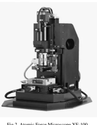
The coated sample is investigated by AFM for determining the elastic moduli and hardness by a process called combined Nanoindentation and scratching. The AFM experimental set up consists of a laser resource to incident on the sample surface held on an XYZ scanner. The scanner with the sample head can be moved in XY- horizontal plane. The Silicon cantilever located above the sample with a probe (tip of SiC) at its end is used to indent and scratch over sample surface. The tip is of parabolic shape with a radius of 10 nm. The experimental set up of the AFM XE-100 is shown in Figure-2
The chromium carbide (Cr3-C2) coated sample has been placed on the Scanner surface and focuses the
AFM contact mode has been used to indent and scratch the sample surface. The maximum load that can be applied on the cantilever is 20 nN
Fig 2 Atomic Force Microscope XE-100.
The tip is vibrated in the horizontal X-direction with a forward (down) velocity of 0.3 µm / sec and for a time period of 6.67 sec. The tip also moves in backward direction with the same velocity. The maximum force that can be applied by the tip is 14.5 nN. Four different locations are chosen to apply the load and scratch the surface. The applied load is from few pN to few nN. The image capturing and analysis of the data is obtained by a monitor with the help data acquisition software. The measured data consists of surface topography, surface roughness, force-displacement curves and the values of Elastic moduli and hardness that are discussed in Results and Discussions section.
Figure-3 The image of vibrating tip displayed by Data acquisition software.
3. THEORY OF NANO SCRATCHING AND INDENTATION
not only moves in lateral direction but also penetrates into the sample surface. Thus, in Nanoscratching, the sample is also indented through few nm to µm depth of the sample. By measuring the resistance offered by the surface, the mechanical properties like Young’s modulus and Hardness can be determined.
3.1 Surface Topology
The surface topology of an AFM image consists of measurement of surface roughness, waviness and texture. Solid surfaces, irrespective of the method of formation, contain surface irregularities or deviations from the prescribed geometrical form. When two nominally flat surfaces are placed in contact, surface roughness causes contact to occur at discrete contact points. Deformation occurs in these points, and may be either elastic or plastic, depending on the nominal stress, surface roughness and material properties. The sum of the areas of all the contact points constitutes the real area that would be in contact, and for most materials at normal loads, this will be only a small fraction of the area of contact if the surfaces were perfectly smooth. AFM has been used to measure surface roughness on length scales from nanometers to micrometers.
Surface roughness is most commonly characterized by the standard deviation of surface heights, which is the square root of the arithmetic average of squares of the vertical deviation of a surface profile from its mean plane. Due to the multiscale nature of surfaces, it is found that the variances of surface height and its derivatives and other roughness parameters depend strongly on the resolution of the roughness-measuring instrument .A unique property of rough surfaces is that if a surface is repeatedly magnified, increasing details of roughness are observed right down to the nanoscale. The various roughness parameters are described below.
Average Roughness (Ra)
The Average Roughness is the arithmetic average of the absolute values of the surface height deviations measured from the mean plane. When “Roughness” analysis is applied to an image, the image data is automatically plane fitted beforehand. Regarding basic roughness measurements, average roughness Ra is one of statistics used by the roughness routine are derived from ASME. While Image Mean value of data contained within the image, Image Ra Arithmetic average of the absolute values of the surface height deviations measured from the mean plane is given by
==
N 1 j j aZ
N
1
R
--- (1)Where,
Z
j corresponds to height of a particular surface ‘j’ and N is the number of surface heights.The Root Mean Square value of Surface Roughness (Rq)
The image RMS (Rq) is the root mean square average of height deviations taken from the mean data plane and is expressed as:
N
Z
R
2 i
q
=
--- (2)Similarly, the other parameters include the average maximum height of the profile (Rz) and the difference (Rp)
between the lowest and highest points on the surface
In AFM, the cantilever defection versus the height position of the sample is recorded by force curves. The force distance (FD) curve is defined by using an absolute distance, which is the separation between the tip and sample surface, instead of using sample position (Z). According to Hertz model, if the tip of AFM is approximated as a sphere then the force on the cantilever (F) can be calculated by [14]
(
)
322
sphere
R
δ
ν
1
E
3
4
F
−
=
--- (3)Where E is the elastic modulus of the sample, R is the radius of the probe sphere ,
δ is the indentation deprth and ν is the poisson ratio.
The hardness H of the sample can be found out by dividing the maximum indentation load with the contact area of the indenter. For a parabolic indenter the hardness H is given by
2
3
cc
h
A
max max
F
F
H
=
=
--- (4)Where Ac is the contact area and hc is the contact or indentation depth.
4. RESULTS AND DISCUSSIONS
4.1 Surface topography
Figure-4 represents 2-Dimensional (2-D) AFM image of Cr3-C2 coated sample after combined
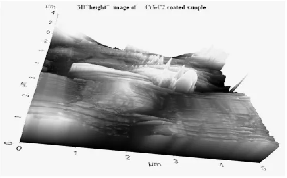
nano scratching and nano indentation in an area of 5 µm x 5 µm on sample surface. The image is obtained during the contact mode of AFM. The image shows the irregularities in the arrangement of surface atoms due to the composite properties of the constituents of the coating. The variation in height of peak profile is described by roughness value. The 3-D AFM image of the composite coating along with the surface height is shown in Figure-5.
z
Figure -5 AFM 3-D “Height” Image of Cr3-C2 coated sample
4.2 Surface roughness
The roughness parameters are estimated by analyzing the topography scan of the sample surface. Scan over 5 µm x 5 µm are taken and the AFM image corresponding to roughness measurement of the Cr3-C2
(75-25%) coated sample is shown in Figure-8. The roughness values of Cr3-C2 are measured over a rectangular area
in horizontal plane. The average roughness (Ra), Root Mean Square roughness (Rq), average maximum height of
the profile (Rz) and the difference (Rp) values of the coated sample is shown in Table-1. The measurement of
surface roughness is obtained with the histogram and a line profile along with AFM image. The surface shown in Figure-8 is with sharp bumps on it and is due to irregular grains which got stuck in the surface. These bumps seem to be broader when probed with AFM tip. This is further highlighted by the more number of burrs present in the topographical image shown in Figure-8.
Figure- 8 AFM Image of surface roughness along with histogram and a line profile of coated Cr3-C2 (75-25%) sample.
Table-1 Surface roughness values of (Cr3-C2) coated sample.
Meuasured Surface roughness parameter
Coated Material Ra (µm) Rq (µm) Rz (µm) Rp (µm)
Cr3-C2 (75-25%) 0.166 0.187 0.520 0.627
4.3 Mechanical properties
The mechanical properties of the coated sample is obtained by analyzing the Force-distance curve obtained during scratching and indenting the sample. In the present study, the elastic modulus and hardness of the coated sample is obtained by indentation. The cantilever tip is contact with sample surface, where the nanoindentation and nanoscratching is carried out indirectly at four different places. The AFM tip is vibrated with a velocity of 0.3 µm/sec for a time period of 6.67 seconds in lateral direction. ν is the poisson ratio of coating material is 0.5. After finding the suitable location, while the tip is scratched over the surface, it also penetrates through a particular depth. By measuring the depth of penetration and the force applied on the tip, the elastic modulus and hardness of the sample material is estimated by the Hertzian analytical model.
In the present investigation, the tip is scratched at four different places on a scan surface of 5 µm x 5 µm in order to find out the resistance due to penetration. For e.g., at point 1 (Figure-9 (a)) on the sample surface, the tip is scratched at a distance of 1.445 µm in X-direction and 1.562 µm in Y-direction. The obtained force vs. Z detector distance is shown in-Figure-9 (b). The initial and final positions of the cursor corresponding force and depth are indicated red and green color pointed triangles as shown in Figure-9 (b).
For a parabolic indenter with a radius of 10 nm, the obtained indentation depth, Young’s modulus and hardness of the Cr3-C2 (75-25%) sample with other parameters at four different locations are summarized in
(a) Location of scratching (b) Force vs.Z Detector distance.
Figure-9: Force-Z Detector curve of Coated Cr3-C2 (75-25%) sample.
Table-2 Mechanical properties with indentation parametrs of coated sample.
Location Parameter Indentation depth
(nm)
Force (pN)
Young’s modulus (Pa)
Hardness (Pa)
Point 1 310.72 2.214 71.89 6.63 Point 2 242.2 11.805 557.09 58.18 Point 3 214.72 6765 382460 42420 Point 4 48.79 3728 1950000
452770
The Force-indentation depth (F-D) curves obtained for Cr3-C2 (75-25%) coated sample is shown in
Figure-10. The force-depth data follows the Hertzian analytical equation-(3) and (4) in evaluation of Young’s modulus and Hardness values. The data displayed in Table-2 of Young’s modulus and hardness are obtained directly from the experiments using equation-(3) and (4). The Young’s modulus of the Cr3-C2 (75-25%) sample is found
Figure-10: Force vs. Indentation depth (Cr3-C2 (75-25) coated sample)
It is clear from the results that the analytical experimental values are in good agreement. Therefore, the results are validated.
5. CONCLUSIONS
Due to the advent in materials and their superior properties, the research in NanoTechnology has been focused to Nano composite coatings of chromium Carbide. In the present work, the chromium Carbide composite coatings (Cr3-C2 (75-25%)) has been investigated to obtain the surface topology, surface roughness
and mechanical properties young’s modulus and Hardness. The coating has been deposited by detonation gun spray process on Aluminium samples. An Atomic Force Microscope (AFM) in contact mode has been used to scratch and indent the sample surface through few nanometers depth. The average roughness value of the (Cr3
-C2 (75-25%)) sample is 0.166 µm. The Young’s modulus and hardness of (Cr3-C2 (75-25%)) coated sample is
in the range of 583.27 kPa and 123.8137 kPa. ν is the poisson ratio of coating material is 0.5. The results obtained from experimental work for Force-displacement data and other mechanical properties are validated with Hertz analytical results. The results are in good agreement.
REFERENCES
[1] R.Bassani, R. Solaro, M. Alderighi and C. Di Ceasare, proceedings, Nanoscratching Nanoindentation with AFM, International Conference on Tribology,Italy, PP.20-22 September 2006.
[2] Yu-Ju Chen, Ju-Hung Hsu and Heh-Nan Lin, Fabrication of metal nanowires by atomic force microscopy nanoscratching and lift-off process, Nanotechnology, 16, PP.1112–1115, 2005.
[3] Xiaoliang Shi, Gangqin Shao, Xinglong Duan, and Runzhang Yuan, Atomic Force Microscope study of WC-10Co Cemented Carbide sintered from Nanocrystalline composite powders,Journal of University of Science and Technology Beijing Vol. 12, No.6, PP.558-563, 2005.
[4] Wen-Yang Chang, Te-Hua Fang,and Chun-Nan Fang, Molecular Dynamics on Interface and Nanoscratch Mechanisms of Alkanethiol Self-Assembled Monolayers , J. Physical Chemistry B, 113, PP. 14994–15001, 2009.
[5] Jyh-Wei Lee, Jenq-Gong Duh, Nanomechanical properties evaluation of chromium nitride films by nanoindentation and nanowear techniques, Surface & Coatings Technology, 188–189, PP. 655– 661,2004.
[6] Z. Zak Fang , Xu Wang, Taegong Ryu, Kyu Sup Hwang, H.Y. Sohn, Synthesis, sintering, and mechanical properties of nanocrystalline cemented tungsten carbide – A review, Int. Journal of Refractory Metals & Hard Materials, 27, PP.288–299, 2009. [7] Binyang Du, Mark R. VanLandingham, Qingling Zhang and Tianbai He, Direct Measurement of Plowing Friction and Wear of a
Polymer Thin Film using the Atomic Force Microscope, J. Materials Research., Vol. 16, No. 5, PP.1487-1492, 2001.
[8] J. O. Carneiro, V. Teixeira A. Portinha, S. N. Dub and R.Shmegera, Hardness Evaluation of Nanolayered PVD Coatings using Nanoindentation, Review of Advance Materials Science, 7, PP. 83-90, 2004.
[9] M. S. Bobji and S. K. Biswas, Estimation of Hardness by Nanoindentation of Rough Surfaces, Journal of Materials Research, PP. 3227-3233, 1998.
[10] X.N. Xie , H.J. Chung, C.H. Sow, A.T.S. Wee, Nanoscale Materials Patterning and Engineering by Atomic Force Microscopy Nanolithography, Materials Science and Engineering R 54, 1–48, 2006.
[11] L. Santinacci T. Djenizian and P. Schmuki, A Semiconductor Nano-Patterning Approach Using AFM-Scratching Through Oxide Thin Layers, Materials Research Society Symposium, Vol. 740, 2003.
[12] Ch.Srinivasa Rao, and C.Eswara Reddy, An FEM Approach into Nanoindentation on Linear Elastic and Visco Elastic characterization of Soft Living Cells, PP 55-68, No 1, Vol 2, International journal of Nanotechnology and Applications, 2008
[13] Ahmed Touhami, Bernard Nysten, and Yves F. Dufrene, Nanoscale Mapping of the Elasticity of Microbial Cells by Atomic Force Microscopy, Langmuir, 19, PP.4539-4543, 2003.