Available at http://www.ijcsonline.com/
Bandwidth Enhancement Techniques using Stacked Microstrip Patch Antennas
Mr. G.Sreedhar Kumar1, Mr. J. Anil kumar2, Mr. C. Mahesh babu3, Mr. Md. Furqan ahmed4, Mr. K. Harinath5, Mr. P. Guru Prasad6
1Sr.Asst Professor, Department of ECE, GPCET, Kurnool, India 2,3,4,5,6Student, Department of ECE, GPCET, Kurnool, India
Abstract
Microstrip patch antennas are widely used because of their many advantages, such as the low profile, light weight, and conformity. However, patch antennas have a main disadvantage i.e. a narrow bandwidth. Researchers have made many efforts to overcome this problem and many configurations have been presented to broaden the bandwidth. A new, compact, simple and gap coupled broadband microstrip patch antenna with multilayer stacked configuration is presented in this paper. The computer simulation results show that the antenna can realize wide band characters. The Return loss, smith chart, impedance, radiation pattern, gain, VSWR and directivity of such an antenna are studied. The possibility of increasing bandwidth, gain and directivity of the microstrip patch antenna using line feed techniques is examined. Percentage bandwidth of antenna is approximately calculated using line feed technique. ANSOFT HFSS 13.0 is used in order to design the antenna and simulate the antenna characteristics.
Keywords: Stacked Microstrip Antennas, Return Loss, Bandwidth, Ansoft HFSS Simulation Tool.
I. BANDWIDTH ENHANCEMENT TECHNIQUES
A variety of broadBand techniques have been developed using the three approaches categorized below. It is known that the factors affecting the bandwidth of a Microstrip Patch patch antenna are primarily the shape of the radiator, the feeding scheme, the substrate and the arrangements of radiating and parasitic elements. Out of all the different broadBand techniques we had as stated in the table 1.1 the present thesis specifically covers the variation in the bandwidth of the Microstrip Patch antennas when the stacked antennas (parasitic or coplanar) are employed in the design. The approaches are as shown below
1. Lowering the quality factor 2. Use impedance matching 3. Introduce multiple resonances .
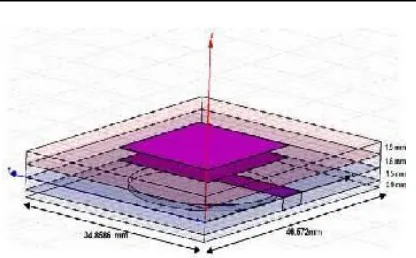
Stacked Arrangements:
Introducing multiple resonances can be done by stacked arrangements. Figure shows arrangements whereby parasitic elements are placed above the main patches. By dint of the coupling between stacked elements and the driven element, the impedance bandwidth can be increased greatly. Usually, for VSWR=1.5 the bandwidth can reach 10–20%, particularly as the medium between the upper and bottom patches is air or a material with low permittivity.
Fig 1. Stacked patch Antenna Structure
II. MICROSTRIP PATCH ANTENNAS
A. Overview of Microstrip Patch Antenna
control and so on. These characteristics can be achieved by suitably loading simple micro strip antennas. These antennas are becoming more commonly used in such applications.A microstrip antenna is defined by its Length, Width, Input impedance, and Gain and the radiation patterns.
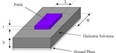
A Microstrip patch antenna (MPA) consists of a radiating patch on one side of a dielectric substrate which has a ground plane on the other side is shown in Figure 2. The patch is generally made of a conducting material such as copper or gold and can take any available shape. Radiating patch and the feed lines is usually photo etched on the dielectric substrate.
Figure 2: Structure of a Microstrip Patch Antenna
The patch contains variety of shapes the commonly used shapes are square, elliptical, circular, rectangular and triangular or some other common shapes are shown in Figure 3.
Figure 3: Common shapes of micro strip patch elements Microstrip patch antennas radiate primarily because of the fringing fields between the patch edge and the ground plane. For improving the antenna performance a thick dielectric substrate having a low dielectric constant is desirable since it gives a good efficiency, widebandwidth and better radiation pattern but such configuration leads to a larger antenna size. So in order to design an optimized micro strip patch antenna the substrates with higher dielectric constants must be used which are less efficient and result in narrower bandwidth. Hence there must be trade-off between the antenna dimensions and antenna performance.
B. Feed Techniques
Microstrip patch antennas can be fed by different types of methods. These are grouped into two categories- contacting and non-contacting.
In the contacting method, the RF power is fed directly to the radiating patch using a connecting element such as a micro strip line. In the non-contacting scheme,
electromagnetic field coupling is done to transfer power between the microstrip line and the radiating patch. The most popular feed techniques are the micro strip line, coaxial probe and coplanar waveguide these are comes under contacting schemes. And proximity coupling, aperture coupling are the non-contacting schemes.
Fig 4 Feeding Techniques
Microstrip Line Feed : In this type of feed technique,
a conducting strip is connected directly to the edge of the Micro strip patch .The conducting strip is smaller in width as compared to the patch and this kind of feed arrangement has the advantage that the feed can be etched on the same substrate to provide a planar structure. The purpose of the inset cut in the patch is to match the impedance of the feed line to the patch without the need for any additional matching element. This is achieved by properly controlling the inset position. Hence this is an easy feeding scheme, since it provides ease of fabrication and simplicity in modelling as well as impedance matching. However as the thickness of the dielectric substrate being used, increases, surface waves and spurious feed radiation also increases, which hampers the bandwidth of the antenna. The feed radiation also leads to undesired cross polarized radiation.
C. Advantages and Disadvantages of Microstrip patch Antenna:
Microstrip patch antennas are increasing in popularity for use in wireless applications due to their low profile. They are more compatible for embedded antennas in handheld wireless devices such as cell phones, pagers etc... The communication antennas on missiles need to be thin and conformal and are often in the form of Microstrip patch antennas. In satellite communications also these antennas are widely used. The principal advantages of the patch antenna are given below:
Less weight and low volume.
Low profile so that these are easily conformal to host surface.
Less fabrication price.
CP and LP (polarizations) are possible.
It can easily embed on any type of the microwave integrated circuits (MICs).
Patch antennas suffering from some disadvantages are given below:
Narrow (or) less bandwidth. Efficiency of patch antenna is less. Gain is low.
Power handling capacity is low. Spurious surface wave excitation.
Microstrip patch antennas have a very high antenna quality factor (Q). It represents the losses associated with the antenna where a large Q leads to narrow bandwidth and low efficiency. The value of Q is decreased by increasing the thickness of the dielectric substrate. But the thickness the total power delivered by the source goes into a surface wave is also increases. This gives unwanted power loss since it is ultimately scattered at the dielectric bends and causes degradation of the antenna characteristics. Narrow bandwidth and fire radiation can be overcome by choosing appropriate feeding technique. In this project CPW feeding is used to get the wider bandwidth.
III. DESIGN OF ANTENNA
The proposed designs for increasing the bandwidth of the antennas are mentioned as below. The designs are carried out in ANSOFT HFSS with the following parameters :
Substrate used: Rogers RT/duroid 5880 Dielectric constant : 2.2
Antenna Patch L=12.45mm, W=16mm Ground L=28mm, W=32mm
Substrate1 L=28mm, W=32mm, H=-0.794 Strip L=2.49mm, W=8mm
Port L=2.49mm, H=0.794
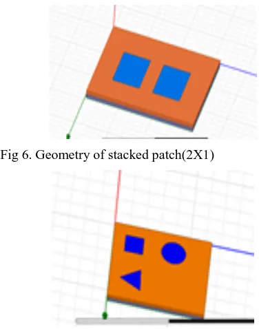
Feeding technique used: Line feeding Parasitic Patch1 L=12mm, W=8mm Parasitic patch2 L=12mm, W=8mm Substrate2 L=28mm, W=32mm, H=0.794
Fig 5. Geometry of microstrip line feed Patch
Fig 6. Geometry of stacked patch(2X1)
Fig 7. Geometry of stacked patch with 3 different shapes
Fig 8. Geometry of stacked patch with 4 different shapes(2X2)
IV. SIMULATION RESULTS
The following are the results of the various designed antennas for enhancement of bandwidth
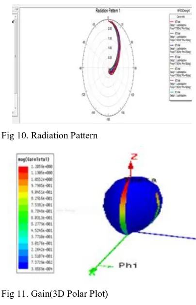
For Stacked Rectangular Patches:
Fig 10. Radiation Pattern
Fig 11. Gain(3D Polar Plot)
Stacked Patches Of Different Shapes:
Fig 12. Return Loss
Fig 13. Radiation Pattern
Fig 14. Gain(3D Polar Plot)
Fig 15: Gain (3D Polar Plot) with four different parasitic elements
V. CONCLUSION
Stacked microstrip patch antenna that has a wide band width in the spectrum was designed by Ansoft HFSS. We used a dielectric constant substrates of 2.2 for a main patch and a parasitic patch. We designed a 2x1 array microstrip antennas and the designs were simulated using HFSS , the results were impressive to see that the bandwidth obtained is 1.17 Ghz compared to the bandwidth obtained from single microstrip antenna which is 0.25Ghz. we also designed single microstrip antenna and 2x1 microstrip antennas with a slot in the driven element and the bandwidth variations are studied. The bandwidth is increased to 1.19 GHz. We also designed multilayered microstrip antennas with different shaped parasitic elements on it and the bandwidth variations , return loss are studied from the simulated results.
REFERENCES
[1] Jennifer, B.T and Carolyn, T.J, "Resonant Frequencies of Rectangular Microstrip Antennas with Flush and Spaced Dielectric Superstrates", IEEE Transactions on Antennas and Propagation, vol. 47, No. 2, 1999, pp. 302-308.
[2] Manfred, K; Rolf, J.H; Koster, H.L, "Accurate model for open end effect of microstrip lines", Electronic Letters, vol.17, 1981, pp. 123-125.
[4] Ramesh, G; Prakash, B; Bahl, I.J; Ittipiboon, A, "Microstrip Antenna Design Handbook", Artech House Inc, Norwood MA, 2001.
[5] Nasimuddin, K.P; Esselle,P; Verma, A.K, "Wideband Circularly Polarized Stacked Microstrip Antennas", IEEE Antennas and Wireless Propagation Letters, vol. 6,2007, pp. 21-24.
[6] G. Sreedhar Kumar, T. Uma Latha, S. Usha, N. Tanuja Latha, Y. Sumitra Sravani Singh, H.K.Sowmya, "Frequency Reconfigurable Triangular Microstrip Patch Antenna for Wireless Applications", International Journal of Computer Systems (IJCS), pp: 277-280, Volume 3, Issue 3, March 2016.
[7] G. Sreedhar Kumar, B. Raghu Nandana Reddy, M. Purushotam Reddy, M. N. B.Venkateswarulu, P. Kumara Swamy, P. Pavan Kumar, "Circularly Polarized Circular Patch Antenna with Coplanar Parasitic Elements", International Journal of Computer Systems (IJCS), pp: 281-284, Volume 3, Issue 3, March 2016. [8] Wong, K.L, "Compact and Broadband Microstrip Antennas", John
Wiley & Sons, NY, 2002.
ABOUT AUTHORS
Mr. G. Sreedhar Kumar, working as Sr.Asst Professor, in Dept of ECE, GPCET, Kurnool. He completed his M.Tech in year 2009. His research area is Microstrip Patch Antennas.
Mr. J. Anil kumar pursuing his final B.Tech in ECE at GPCET, Kurnool. His research area is Microstrip Patch Antennas.
Mr. C. Mahesh babu, pursuing his final B.Tech in ECE at GPCET, Kurnool. His research area is Microstrip Patch Antennas.
Mr. Md. Furqan ahmed, pursuing his final B.Tech in ECE at GPCET, Kurnool. His research area is Microstrip Patch Antennas.
Mr. K. Harinath, pursuing his final B.Tech in ECE at GPCET, Kurnool. His research area is Microstrip Patch Antennas.