Research Article
Active Thermal Sensor for Improved Distributed Temperature
Sensing in Haptic Arrays
D. Cheneler
1and M. C. L. Ward
21Department of Engineering, Lancaster University, Lancaster, UK
2School of Engineering and the Built Environment, Birmingham City University, Birmingham, UK Correspondence should be addressed to D. Cheneler; [email protected]
Received 27 April 2018; Revised 27 June 2018; Accepted 9 July 2018; Published 2 September 2018
Academic Editor: Stefano Stassi
Copyright © 2018 D. Cheneler and M. C. L. Ward. This is an open access article distributed under the Creative Commons Attribution License, which permits unrestricted use, distribution, and reproduction in any medium, provided the original work is properly cited.
The efficacy of integrating temperature sensors into compliant pressure sensing technologies, such as haptic sensing arrays, is limited by thermal losses into the substrate. A solution is proposed here whereby an active heat sink is incorporated into the sensor to mitigate these losses, while still permitting the use of common VLSI manufacturing methods and materials to be used in sensor fabrication. This active sink is capable of responding to unknown fluctuations in external temperature, that is, the temperature that is to be measured, and directly compensates in real time for the thermal power loss into the substrate by supplying an equivalent amount of power back into the thermal sensor. In this paper, the thermoelectric effects of the active heat sink/thermal sensor system are described and used to reduce the complexity of the system to a simple one-dimensional numerical model. This model is incorporated into a feedback system used to control the active heat sink and monitor the sensor output. A fabrication strategy is also described to show how such a technology can be incorporated into a common bonded silicon-on-insulator- (BSOI-) based capacitive pressure sensor array such as that used in some haptic sensing systems.
1. Introduction
There are many variants of silicon-based sensors available
today [1–3]. Many of the compliant sensors, in particular
strain and pressure sensors, require temperature
compensa-tion in order to mitigate thermal expansion effects [2]. As
such, many designs incorporate some manner of structure to prevent/correct for thermal expansion [4] or some manner of temperature sensor, usually a temperature-sensitive resis-tor, to facilitate correction of the sensor output [5, 6]. In gen-eral, these integrated temperature sensors do not provide a measure of the actual ambient temperature, but rather the temperature of the compliant sensor, which is a function not only of the ambient temperature but also of thermal losses through the substrate. However, there are several instances where one is interested in the temperature not to simply correct other sensors, but to provide an additional sensing modality. A typical scenario where this applies is with haptic arrays where one may wish to incorporate an array, sometimes hundreds, of compliant pressure sensors
into some manner of robotic end effector to monitor contact
and facilitate the handling of objects [6–9]. Temperature
sen-sors are often incorporated into these arrays to provide a more biomimetic sensing modality [10, 11].
As with the pressure sensors, there are many variants of thermal sensor available [12]. One of the most common devices for temperature measurement is the temperature-sensitive resistor or resistance temperature detector (RTD)
[13, 14]. Generally consisting of a thin wire, afilm of highly
conductive metal such as platinum, or an area of highly
doped silicon, RTDs have been found to offer better accuracy
and repeatability over alternative sensors such as thermocou-ples [15]. The resistance ideally varies linearly with
tempera-ture, although the self-heating effects need to be considered
[16]. However, if every pressure sensor in a large haptic array requires individual conventional temperature sensors or a commercial RTD located next to it, then the spatial resolu-tion of the tactile sensor will be severely undermined. By inte-grating a micro thermal sensor into the same substrate as the pressure sensor, the temperature-dependent error of the
pressure sensor can be minimised without dramatically
affecting the resolution of the array and still allow an accurate
measurement of the ambient temperature. Using existing designs, such a sensor, however, will be very sensitive to its environment, in particular the substrate, due to the previ-ously mentioned thermal losses.
This paper is aimed at addressing this issue through the incorporation of a microactive heat sink that acts as an intermediate structure between the thermal sensor and the substrate. The system is designed to be suspended away from the substrate in a similar manner to many silicon-based pressure sensors, especially capacitive diaphragm-based sensors [4, 17, 18], so that it can be fabricated in much the same way. The fabrication method is detailed below. Both the thermal sensor and active sink are thermoelectric
ele-ments that are sensitive to the thermal energy thatflows in
and out of the respective elements; however, the active sink actively responds to losses from the sensor into the substrate and compensates accordingly by providing the equivalent power back to the sensor in real time. This allows the thermal sensor to behave as though it is thermally isolated from the substrate below, ensuring its output is only a function of
the external ambient temperature/heat flux. The system is
analytically and numerically modelled below to elucidate its
thermodynamic behaviour and to justify simplified
one-dimensional expressions that are then used in the feedback system. This feedback system is used to control the output of the active heat sink automatically and monitor the thermal sensor output.
2. Basic Design
The pressure sensors used in a tactile array are often
diaphragm-based capacitive sensors [17–20] whereby the
external contact force deflects the diaphragm changing the
gap between it and the substrate, resulting in a change in capacitance between the two. A typical silicon-based design is shown in Figure 1. While many equivalent designs are possible, for simplicity it is assumed here that the pressure sensor was fabricated on a bonded silicon-on-insulator (BSOI) wafer coated with a polymer layer for protection with the diaphragm being released through selective etching of the insulating oxide layer. The theory that follows is appli-cable for many, not necessarily silicon-based, equivalent designs, provided that the sensor consists of two conductive elements (the diaphragm and substrate) separated by an electrically, but not thermally, insulting layer (the oxide layer in this example).
The thermal sensor would need to be as close as possible to the pressure sensor in order to reduce the size of the array and to make accurate measurements without introducing too many additional fabrication steps. Therefore, the thermal sensor will ideally be fabricated on the same layer as the sili-con diaphragm. However, a simple temperature sensor com-prising of a thin wire of silicon etched out of the device layer
of the BSOI will not suffice. This is due to the high thermal
conductivity of both silicon and its oxide. If the silicon sub-strate is maintained at room temperature, any heat energy supplied through the polymer layer will be lost immediately to the substrate and the temperature sensor will not work as intended. A heating element at the same temperature as the ambient temperature located between the sensor and the substrate would mean that the temperature gradient across the sensor would be zero and no heat will be lost. This can be achieved if the sensor is fabricated on top of an
“active sink.” Both the sensor and the active sink will be
maintained at a constant, slightly elevated, temperature by monitoring their resistance and controlling the voltage pass-ing through them so that their resistance is maintained at a
predefined value. A schematic of a typical temperature
sen-sor is shown in Figure 2.
This schematic is the simplest configuration of the active
sink design. In practice, one would wish the thermal sensor
and its sink to be much stiffer than the pressure sensor to
avoid contact with the substrate while under load. This can be achieved by making the sensor short. This will reduce the resistance and so one may wish to have several of these elements acting together like a long thermal sensor with higher resistance supported by several intermediate islands of oxide. These designs are all equivalent, and the theory below applies to them all.
3. Theory
It has been known for a long time that the passage of an elec-tric current through a conductor releases heat. The
phenom-ena was first studied by James Joule in 1841 [21], and the
equation for the temperature in a thin wire through which
a constant current isflowing was found by Verdet in 1872
[22]. It was discovered that the mechanisms behind both electrical and thermal conduction were inextricably linked. It is now known that Joule heating, or resistive heating, is caused by interactions between the moving current and the charged atoms that make up the body of the conductor. Charged particles in the electric circuit are accelerated by
an electricfield but give up some of their kinetic energy each
Protective polymer
layer
Insulating oxide
Gap for capacitance measurement Silicon
diaphragm
Silicon substrate
time they collide with an ion. The increase in the kinetic or vibrational energy of the ions manifests itself as heat and a rise in the temperature of the conductor. Hence, energy is transferred from electrical power to the conductor and any materials with which it is in thermal contact [23]. This trans-fer of energy through molecular interaction is very similar to that accomplished through heat conduction, except in this
case the motion is not necessarily caused by an electricfield
but through momentum exchange from a molecule with a higher energy level [24].
In general, this is a three-dimensional thermoelectric problem. However, as will be shown, the problem reduces to a simpler one-dimensional problem. The schematic for
the simplified model is shown in Figure 3.
As can be seen in Figure 3, the device can be considered to be a simple layered structure. The top layer, the protective polymer, is an insulating layer between a surface set at the external temperature and a surface at the temperature of the sensor. The sensor is a highly conductive thin layer which
has a currentflowing through it. There is heat energy being
generated within the sensor due to electrical resistance and energy exchange through the polymer and insulator layers. The insulating layer is similar in nature to the polymer layer except that the external temperatures are dictated by the tem-perature of the sensor and active sink, respectively. The active
sink is another highly conductive thin layer with a current
flowing through it. Again, heat energy is generated due to
the electrical resistance and energy is exchanged through the insulation layer. However, an additional complication is that energy is also lost from the ends of the sink through the oxide as well as from the surrounding air.
The method for solving this problem was to treat the four
layers as four coupled partial differential equations, which
could then be solved numerically. The governing differential
equation for a one-dimensional transient conduction prob-lem with internal energy generation is given by [25]
k∂
2T
∂x2 +q=ρCp ∂T
∂t , 1
wherekis the thermal conductivity of the layer inW/ m⋅K ,
T is the temperature distribution within the layer inK,qis
the rate of heat energy generated within the layer per unit
volume,ρis the density inkg/m3, andC
pis the specific heat
of the material in J/ kg⋅K . This essentially means,
consid-ering just a small element of material within the layer,
Rate of energy
conduction into
element
−
Rate of energy
conduction out
of element
+
Rate of energy
generation
within element =
Rate of accumu‐
lation of energy
within element
2
In the protective polymer layer, there is no internal heat generation and the temperature gradient within is completely determined by its initial temperature distribution and boundary conditions. The initial temperature distribu-tion is assumed to be constant and at room temperature as will be the case before the device is turned on, and any changes to the external temperatures have been made. The boundary conditions are the temperatures of the outer
Surrounding media, for example, substrate and air maintained
at room temperature Power in
to sensor
Power in to sink
Protective polymer
Sensor
Insulator
Sink External temperature
Figure3: A schematic of the one-dimensional representation of the temperature sensor with active sink. The temperature variation will be in the vertical direction.
Protective polymer
layer
Supporting oxide
Air gap for thermal insulation Active sink
Silicon substrate Insulating polymer Gold film
Supporting oxide Active sink
Gold film
surface and of the sensor. Given this, the differential equation governing this layer is
∂T ∂t =α
∂2
T
∂x2, 3
whereα=k/ρCpand is known as the thermal diffusivity and
is expressed inm2/s. This equation is known as Fick’s second
law and is essentially the diffusion equation [24]. Analytical
solutions exist for this equation as shown in Appendix A; however, numerical integration of the highly oscillatory inte-grals found in the solution means that the solution required extensive computation time and so is not very convenient for further numerical analysis. It is far more convenient in this case to solve (3) fully numerically using the Crank-Nicolson method as described in Appendix B [26]. The solu-tion for the transient temperature distribusolu-tion for the insula-tion layer is found in exactly the same way, with the end temperatures set by the temperature of the active sink and sensor, respectively.
The sensor has a high thermal conductivity and is very thin compared to the surrounding materials. This means that
it can be assumed that the temperature at any instant is eff
ec-tively constant throughout the layer. In this case, the layer is
known as being “thermally thin”[27]. From (2), it can be
seen that the governing equation becomes
ρCpv ∂T
∂t =qin−qp+qv, 4
wherevis the volume of the layer,qin is the energy entering
via the insulator, and qp is the energy being dissipated
through the polymer layer. Naturally, the signs of qin and
qp depend on the instantaneous temperature distributions
within the respective layers and so may change. The energy
exchange,qi, through the relevant layers is due to conduction
which is described by the Fourier rate equation:
qi=kA∂T
∂x, 5
whereAis the area of the layer in thermal contact with the
other layer. The rate of generation of heat due to electrical
resistance in a conductor can be calculated by Ohm’s law:
P=qv=VI=V
2
R , 6
wherePis power in watts,Vis the voltage across the sensor,
andIandRare the current through the sensor and the
resis-tance of the sensor, respectively. As no other work is being done, all the energy generated as electrical power is dissipated as heat. It is assumed that the resistance will be linearly dependent on temperature as shown in (7). This assumption is reasonable over small ranges of temperature.
R=ρeL Ac
1 +aΔT , 7
whereρeis the initial resistivity of the sensor at room
temper-ature measured inΩ⋅m,Lis the length of the conductor inm,
Acis its cross-sectional area inm2,ais the temperature coeffi
-cient of resistance for the layer measured in 1/K, and ΔT
is the change in temperature of the layer from room tem-perature. Therefore, the equation to solve for the response of the sensor can be shown to be
∂T ∂t =
1 ρCpv kA
∂T
∂x in− kA ∂T ∂x p+
V2
ρeL/Ac 1 +aΔT
v
8
As was mentioned above, the active sink behaves in a manner similar to the sensor. This means the governing equation for the sink is the same as (4). It is also assumed that the heat exchange to the insulation layer and to the air is of the same form as (5) and that the resistance of
the sink varies in the same manner as (7). The difference
lies in the exchange of heat to the substrate. Whereas the sensor is in complete thermal contact along its length with the polymer and insulator layer, the active sink is only in contact to the substrate at the ends. This was deliberate in order to reduce the amount of heat loss from the sink. The consequence of this decision is that there is a temperature distribution along the length of the sink. For example, consider an active sink comprised of silicon, with a potential of 1 V applied across it, of dimensions
1000×100×2μm connected to a substrate maintained at
room temperature via silicon blocks of 150×150×2μm
on top of silicon dioxide blocks of 50×50×2μm as shown
in Figure 4. The silicon was assumed to be doped to satu-ration with arsenic to make it electrically conductive. The properties of the silicon and its oxide are given in Table 1. As can be seen in Figure 4, the thermoelectric problem for the active sink has been solved using COMSOL 4.3, a commercial FEA package [28]. The results show that there
Oxide
Max: 313.03 K
Min: 293 K
is a temperature distribution along the length of the sink in a
direction perpendicular to the assumed direction of heatflow
as dictated in Figure 3. This is because the dominant heat loss mechanism in the active sink is conduction through the ends of the sink to the substrate below, which is maintained at room temperature. In order to reduce this problem to the required equivalent one-dimensional problem, it is necessary to ensure that the relevant heat exchange mechanisms are the same for both cases. Plotting the steady-state temperature distribution for the active sink in a more convenient form, see Figure 5, shows that the temperature distribution is essentially parabolic in nature. This means the temperature distribution can be assumed to have the form
dTd y =dT0 1 + 4
y L−
1 2
2
+dTend, 9
wheredTd y is the horizontal temperature distribution in
the horizontal direction, y, along the length, L, of the
active sink.dTendis the difference between the temperature
of the ends of the sink and room temperature, and dT0 is
the difference between the peak temperature in the sink
and Tend.
In order to be consistent, the energy converted from elec-trical to heat needs to be the same in the two-dimensional
and one-dimensional cases. The electrical power passing through the sink is given by combining (6) and (7). In the one-dimensional case, it is assumed that the temperature
dif-ference is constant throughout the sink, that is, ΔT=dTc,
and so the power can be given as
P=I2ρeL Ac
1 +a dTc 10
In the two-dimensional case, the temperature distribu-tion has to be taken into account. In this situadistribu-tion, the power can be expressed as
P=
L
0
I2ρeL Ac
1 +a dT0 1 + 4
y L−
1 2
2
+dTend dy
11
Equation (11) can be solved to give
P=I2ρeL Ac
1 +a 2
3dT0+dTend 12
In order that the energy generated due to electrical resis-tance is the same in both cases, (10) and (12) must be equal. Therefore, the relationship between the assumed constant temperature of the active sink and the actual parameters of the temperature distribution is
dTc=
2
3dT0+dTend 13
However, in assuming that the temperature difference
of the sink is dTc, the temperature difference at the ends
of the sink is higher than they should be, that is, dTend.
This would result in apparently more heat energy being lost to the substrate than would actually be the case. In order to ensure that the heat loss is correct, it is necessary
to find the temperature at the end of the sink as a
func-tion of the constant temperature alone. The rate of heat loss due to conduction was given in (5). As in this case,
the heat has to flow through two layers in series to the
substrate and so (5) needs to be rephrased slightly to give the heat loss through one end of the sink as [24]
qend= dTend
uo/kSiASi + to/koAo
, 14
where kSi is the thermal conductivity of silicon, ASi is the
cross-sectional area of the silicon block, uo is the distance
from the end of the sink to the oxide, ko is the thermal
conductivity of the oxide layer, to is its thickness, and Ao
is the area of the oxide in contact with the substrate. For
the example given, qend is approximately 1 9 × 10⁶dTend.
Due to conservation of energy, the heat flow out of one
end of the active sink must equal the heat flow into the
Table 1: The properties of doped silicon and oxide used in the active sink.
Silicon Oxide Thermal conductivity (W/ m⋅K) 130 1.38 Electrical resistivity (Ω·m) 0.00006 10e12 Temperature coefficient of resistance (1/K) 0.0005 0 Specific heat (J/ kg⋅K) 712 703
Density (kg/m3) 2330 2200
314
312
310
308
306
304
302
300
298
296
T
em
p
era
tur
e (K)
0 0.1 0.2 0.3 0.4 0.5 0.6 0.7 0.8 0.9 1
Distance along sink (mm)
silicon block as given by (14). Applying (5) to the end of the active sink gives
qend=kSiAc
∂ T0 1 + 4 y/L − 1/2 2
+Tend
∂y 15
By solving (15) for the two ends of the active sink, we obtain
qend=
4kSiAc
dT0
L , y= 0,
−4kSiAc
dT0
L , y=L
16
Equating (16) for the case ofy= 0 with (14) gives the
relationship
dT0=
dTend
uo/kSiASi + to/koAo L
4kSiAc
17
This can be substituted into (13) to give the tempera-ture of the end of the active sink as a function of the pre-sumed constant temperature
dTend=dTc
1
uo/kSiASi + to/koAo
L
6kSiAc
+ 1
−1
18
Therefore, the heat loss due to conduction to the sub-strate can be given as
qend= 2 dTc
uo/kSiASi + to/koAo
1
uo/kSiASi + to/koAo
L
6kSiAc
+ 1
−1 19
Here, a factor of two is included because, of course, the heat is being lost out of both ends of the active sink. In a similar fashion to (8), the equation governing the response of the active sink can be shown to be
∂T ∂t=
1
ρCpv
kA∂T ∂x in−2
dTc
uo/kSiASi + to/koAo
1
uo/kSiASi + to/koAo
L
6kSiAc
+ 1
−1
+ V
2
ρeL/Ac 1 +aSidTc
v
20
For validation of this last result, (20) was solved in iso-lation using a fourth order Runge-Kutta algorithm in Simulink. For clarity, the term related to the heat exchange through the insulator was omitted. This was then com-pared to the transient response of the isolated active sink calculated using FEA in Comsol shown in Figure 4. In
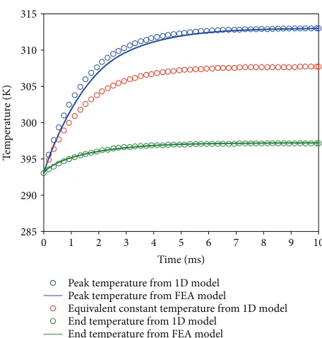
Figure 6, the peak temperature and the end temperature of the active sink as calculated using FEA are compared to the temperatures as inferred from the results of the Simulink simulation and (13) and (18). The equivalent constant temperature as calculated from the Simulink model is also plotted for comparison. It is important to note that it took over twenty minutes to solve the full 3D model of the active sink with FEA and less than ten seconds to solve the equivalent 1D case in Simulink.
In Figure 7, the transient response of the current flow
through the active sink as calculated by the FEA model assuming that the full three-dimensional temperature distri-bution and the equivalent one-dimensional distridistri-bution assumed in the Simulink model are compared. As the tran-sient response of the current and the calculated end temper-atures of the sink are the same in both models, it shows that the two are equivalent with the same amount of energy being generated and lost in both cases. The advantage of using the one-dimensional case instead of using FEA directly is the reduction of computational time and the ease of including feedback systems in the model without reducing accuracy
significantly. Discrepancies are likely to be due to the
assumption that the temperature distribution is parabolic which is only approximately true.
To summarise, it has been shown that the heat exchange through the insulator and protective skin layer can be expressed as (3). It has also been shown that the thermoelec-tric response of the sensor layer and the active sink can be given as (8) and (20), respectively. As the response of one
layer is directly affected by the response of neighbouring
layers, the governing equations are coupled and hence an analytical solution is unlikely. Fortunately, now the problem is in this reduced form, a numerical solution is possible.
315
310
305
300
395
290
285
T
em
p
era
tur
e (K)
0 1 2 3 4 5 6 7 8 9 10
Time (ms)
Peak temperature from 1D model Peak temperature from FEA model
Equivalent constant temperature from 1D model End temperature from 1D model
End temperature from FEA model
4. Feedback System
The purpose of using an active sink as part of the device is to prevent heat loss from the temperature sensor to the
sub-strate. This allows the heatflux through the polymer layer
due to changes in external temperature to be directly mea-sured by the temperature sensor. For this to work, the tem-perature of the active sink and the temtem-perature sensor has to set to the same constant value. This can be seen if (2) is applied to the temperature sensor. If the temperature is kept constant, the rate of accumulation of energy is zero. Simi-larly, if the active sink is at the same temperature as the sen-sor, there is no loss to the substrate. Therefore, if the accumulation and loss of energy is zero, the rate of energy coming into the sensor must equal the rate of energy being
generated. Put more simply, the change in heatflux through
the polymer will equal the change in electrical power needed by the sensor to maintain its temperature; that is, if the external temperature increases, the power through the sensor will decrease.
The feedback control to the active sink and temperature sensor consists of a simple proportional controller. By
mea-suring each element’s resistance at room temperature and
temperature coefficient of resistance, (7) can be used to
deter-mine the resistance of each element at the set temperature. In
the case of this device, the initial specified temperature is to
be set at 37.5°C to be comparable to the body temperature.
During the experiment, the instantaneous resistance of each element is compared to the required resistance and normal-ised and the voltage is changed by the normalnormal-ised resistance multiplied by a gain factor, that is,
V t =V t−dt +dV=V t−dt +GRreq−R t Rreq−Ro
, 21
wheredVis the change in applied voltage,Gis the gain,Rreq
is the required resistance, that is, the resistance calculated
using (7),Rois the resistance at room temperature, andR t
is the instantaneous resistance. In this way, the resistance is
kept constant and hence each element’s temperature. Theflux
coming through the polymer layer is then monitored by mea-suring the electrical power through the temperature sensor. The power through the sink will be essentially constant except at times of rapid external temperature change where there will be a small change before it returns to its usual level. Clearly implementation of more sophisticated feedback systems is quite simple, but not necessary.
4.1. Solution of the Model.As was mentioned previously, the
system model for the entire device can be solved using Simu-link; see Figure 8 for the model. The algorithm is as follows:
(1) Initially, it is assumed that all layers are in thermal equilibrium and are at substrate temperature. There is initially no power going to the active sink and temperature.
(2) In thefirst time step, the resistance of the
tempera-ture sensor and active sink is measured and com-pared to the required resistance equivalent to the
initial specified elevated temperature (37.5°C) and
the voltage is increased accordingly.
(3) This results in a change in temperature of the sink and sensor. Given these temperatures as boundary
conditions, the temperature profile throughout the
insulation and polymer layer is found by solving (3) using the Crank-Nicolson method as discussed in Appendix B. This is achieved using an embedded
Matlab code in Simulink. The heatflux being
trans-ferred to/from the sink and sensor can be found by
differentiating the temperature profile in the
insula-tion/polymer layer, respectively, at the interface as
per (5). This then determines the heatflow into and
out of the electrically heated layers.
(4) The instantaneous temperature of the temperature sensor is then found by integrating (8) using the fourth-order Runge-Kutta solver with discreet time-stepping built into Simulink.
(5) Similarly, the instantaneous temperature of the active sink is found by integrating (20) in the same manner as the sensor.
(6) The temperatures are then used tofind the resistances
of the active sink/temperature sensor using (7).
(7) Given the resistance and the applied voltage, the elec-trical power passing through the sensor is measured using (6).
(8) In the next time step, the resistances are compared again to the desired resistances and the voltages being applied to the active sink/temperature sensor are again changed accordingly. The sequence from step 3 to 8 is repeated for the necessary number of time steps.
3.335
3.33
3.325
3.32
3.315
3.31
3.305
C
ur
ren
t (mA)
0 1 2 3 4 5 6 7 8 9 10
Time (ms)
Data from 1D model Data from FEA model
(9) At some juncture, it is possible that the response to a change in external temperature is needed. The algo-rithm just described is the same except that the boundary conditions stated in step 3 for the polymer layer will change as the external temperature changes.
5. Results
For the purposes of simulation, it will be assumed that the temperature sensor will be made out of a gold layer 200 nm thick and with the same width and length as the active sink. The insulation layer and polymer layer will be assumed to have the same properties as PDMS for simplicity. The
insula-tion layer will be 10μm thick, and the protective polymer
layer will be 100μm. The properties of the layers are shown
in Table 2.
It should be noted that gold was considered as it is com-patible with a number of MEMS fabrication facilities. Other
materials, perhaps with a higher temperature coefficient of
resistance or electrical resistivity, could be used if convenient.
The time,dt, for each integration step is 1μs. The gain for the
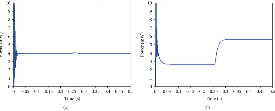
active sink proportional controller was set to 1 and for the temperature sensor was set to 0.05. It was assumed that the controllers would measure the resistances of the pertinent layers and change their voltages accordingly every 0.1 ms. The initial sensor temperature was set to 310.5 K, as before, and the external temperature was set to room temperature (293 K) until 0.25 s when the device was instantaneously brought into contact with an object at 273 K. The response for the active sink and temperature sensor can be that shown in Figure 9.
PSkin
PSensor
PSensor PSkin PInsulator
PInsulatorSensor
PInsulatorSink
PSink
PSink PInsulator PSubstrate
PSubstrate RSink RSensor
Voltage Voltage Tadd
TSensor
TSensor
TSensor
TSensor
TSink
TSink
TSink
TSink Voltage Voltage
RSink RSensor Tadd
Heat exchange through skin
Power in sensor
Power in sink Sensor transience
Heat exchange through insulator
Sink transience
Hear exchange through substrate
Sensor feedback
Sink feedback Power
−K −K
Figure8: The Simulink model depicting how the different layers are linked together.
Table 2: The properties of gold and PDMS as used in the temperature sensor, insulation, and polymer layers.
There are several features that are worth noting in the
response of the active sink and temperature sensor. Thefirst
is the initial transience. As the sink and sensor are starting from room temperature and need to be heated to 310.5 K, there is tendency for the contoller to overshoot before settling down to the correct temperature, especially if the sampling time of the controller is large. It is also important to note that while the temperature was changed instantly, it took the tem-perature sensor about 0.1 s to reach steady state. This is important because the external temperature can only be cal-culated analytically if the temperature gradient throughout the polymer layer is known. Also, while it can be predicted using solutions such as that given in Appendix A, in reality it is likely only to be known exactly when the gradient is con-stant, that is, when the sensor is at steady state. It is interest-ing to note the small increase in power in the active sink before returning to normal as it compensates for the sudden heat loss in the temperature sensor.
It should not be that such changes in power and even the small changes in the resistances of the gold layer are easily achieved using modern digital multimeters, such as NI 4070
[29], which is capable of measuring 1 V at 1μV resolution
and 20 mA at 10 nA resolution and therefore can measure
resistances to ca. 60μ·Ωand powers to 23 nW at the
appro-priate level to seven digits at 5 S/s, which is more than suffi
-cient. Cheaper options can be created using multimeter ICs,
such as MAX1367 [30], to provide a sufficient resolution.
Figure 9(b) shows how the electrical power in the temper-ature sensor changes with external power. Comparing Figure 9(b) with Figure 10 which shows how the heat energy
flowing into the polymer layer changes, it is clearly seen that
the electrical energy is completely converted into heat which
is lost through the polymer layer. This verifies the theory that
the active sink, if maintained at the same temperature as the sensor, does prevent any heat being lost to the substrate.
The effect of the control mechanism can be quite
pro-found. If the sampling rate is too low or the gain is too high,
abhorrent behaviour can occur masking the effects of
chang-ing the external temperature. For example, in Figure 11 the
response of the active sink and temperature sensor is given again for the system described above but with the sampling time increased to 5 ms. Even with the gains for the active sink and temperature sensor controller reduced to 0.5 and 0.05, respectively, the behaviour is not ideal. This will dictate what technology is used for the controllers.
The device temperature was set to 310.5 K which is com-parable to the body temperature and is therefore able to be handled safely. The reason for this high temperature is that
the steady-state temperature difference between this
temper-ature and room tempertemper-ature is 17.5 K which sets the limit for the highest external temperature measureable. It can be seen in Figure 12 that if the external temperature is decreased rel-ative to room temperature, the amount of electrical power converted to heat is increased. Conversely, if the external temperature is increased, the electrical power needed by the sensor to maintain its temperature is decreased. Eventually, the external temperature will be so high that even if no elec-trical power was passing through the sensor, it would still be
10
9
8
7
6
5
4
3
2
1
0
Po
w
er
(
m
W
)
0 0.05 0.1 0.15 0.2 0.25
Time (s)
0.3 0.35 0.4 0.45 0.5
(a)
10
9
8
7
6
5
4
3
2
1
0
Po
w
er
(
m
W
)
0 0.05 0.1 0.15 0.2 0.25
Time (s)
0.3 0.35 0.4 0.45 0.5
(b)
Figure9: (a) The response of the active sink to a change in external temperature of−20 K and (b) the reponse of the temperature sensor.
10
9
8
7
6
5
4
3
2
1
0
Po
w
er
(
m
W
)
0 0.05 0.1 0.15 0.2 0.25
Time (s)
0.3 0.35 0.4 0.45 0.5
at a higher temperature than required and no more increases in temperature can be measured as the power would be zero for all higher temperatures. The minimum external tempera-ture measureable by the sensor will be determined by how much power the control circuit can provide.
The responses given in Figure 12 show a trend which is more clearly seen in Figure 13. Figure 13 shows how the steady-state response changes when the external temperature is changed from room temperature. It can be seen that the
difference in the steady-state power levels in the sensor as
compared to the steady-state power level at room temperature
is a linear function of the change in external temperature. This is likely to be due to the assumption that the resis-tance of the sensor has a linear dependance on tempera-ture as given in (7).
6. Fabrication
As mentioned above, while there are several designs that are possible, they are all equivalent to each other provided that the sensor consists of two conductive elements (the dia-phragm and substrate) separated by an electrically, but not thermally, insulting layer (the oxide layer in this example).
The design configuration below provides an additional
com-mon ground between the detecting layer and the active sink. If the pressure sensor was as described above, that is,
16
14
12
10
8
6
4
2
0
Po
w
er
(
m
W
)
0 0.05 0.1 0.15 0.2 0.25
Time (s)
0.3 0.35 0.4 0.45 0.5
(a)
14
12
10
8
6
4
2
0
Po
w
er
(
m
W
)
0 0.05 0.1 0.15 0.2 0.25
Time (s)
0.3 0.35 0.4 0.45 0.5
(b)
Figure11: (a) The response of the active sink to a change in external temperature of−20 K given a reduction in the sampling rate of the feedback controller to 5 ms and (b) the reponse of the temperature sensor.
15
10
5
0
Po
w
er
(
m
W
)
0 0.1 0.2 0.3 0.4 0.5
Time (s)
dText = 20
dText = 15
dText = 10
dText = 0
dText = −10
dText = −20
dText = −30
dText = −40
dText = −50
dText = −60
Figure12: The responses of the temperature sensor due to changes in the external temperature. dText indicates the difference from room tempertaure (293 K). Note how the time to reach steady state is the same in all cases.
10
8
6
4
2
0
−2
−4
C
h
ange
i
n
p
o
we
r (
m
W
)
−60 −50 −40 −30 −20 −10 0 10 20
Change in external temperature (K)
fabricated on a bonded silicon-on-insulator (BSOI) wafer coated with a polymer layer for protection with the dia-phragm being released through selective etching of the insu-lating oxide layer, as is quite common, then a simple process plan to fabricate the temperature and capacitive sensors together is possible. A possible plan is given in Figure 14.
7. Conclusions
A temperature sensor capable of measuring temperatures
from 40°C to less than−60°C has been described. The sensor
has been designed with the expressed intent of being able to be integrated with existing compliant capacitive pressure sensors. It was noted that if these sensors are silicon-based,
heat loss to the substrate is significant. Therefore, the sensor
incorporates an active heat sink. The active sink and temper-ature sensor have individual proportional controllers allow-ing their temperatures to be maintained at a constant equal value, regardless of the external temperature. By keeping the active sink and temperature sensor at an equal tempera-ture, it has been shown that heat loss from the temperature sensor to the substrate is prevented, so that the change in heat
flux due to change in the external temperature can be directly
and accurately measured.
Even though it is inherently a three-dimensional
struc-ture, the thermoelectrodynamics has been simplified into a
one-dimensional Simulink model which allows for the response of the sensor to be known. The model incorporates
the effect of the temperature profile in the insulation layers as
well as the transient nature of heat generation. In this man-ner, the heat exchange mechanisms between the layers have been fully modelled. The fabrication plan for these sensors has also been described.
Appendix
A. Analytical Solution for Temperature
Distribution in Polymer Layer
As was previously mentioned, (3) does have an analytical solution. In the context of the numerical integration scheme discussed above, only the change in the
tempera-ture distribution, T x , during eachfixed time step, dt, is
required as this gives the heat flux flowing in/out of the
layer’s surface. In general, the temperature distribution
and the associated end temperatures, T1,2, of the
insula-tion/polymer layer are continuous functions of time. How-ever, in the numerical scheme, it is assumed that the end
temperatures are constant for the duration of the fixed
time step. Therefore, the boundary conditions to be used in the solution of (3) are:
T x,t =T1 t′ , whenx= 0,
T x,t =T2 t′ , whenx=L,
A 1
where t′ is the time during each time step, that is, 0≤
t′≤dt. The initial condition is the temperature
distribu-tion, g x , inherited from the solution of the previous time
step. When t= 0, it is assumed that the whole structure is
in thermal equilibrium with the environment and therefore the initial condition can be stated as
T x, 0 =TR, t= 0,
T x, 0 =g x , t> 0, A 2
1. Start with BSOI wafer
2. DRIE to define active sink
3. Use lift off to deposit input electrode on active sink
4. Deposit SU8 for insulation layer
5. Using lift off deposit thermal sensor and ground electrode
6. HF release
whereTR is the room temperature inK. As surface
condi-tions are assumed to be independent of time during each
time step, the general problem can be simplified to that of
two problems, one of steady temperature and one of variable temperature with prescribed initial temperature and zero surface temperature [25]. Put
T=u+w, A 3
whereuandwsatisfy the following equations:
d2u
dx2 = 0 0 <x<L , A 4
u=T1, whenx= 0,
u=T2, whenx=L,
A 5
∂w ∂t =α
∂2w
∂t2 0 <x<L , A 6
w= 0, whenx= 0 andx=L, A 7
w x, 0 =g x −u A 8
Straightaway, the solution to (A.4) can be given as
u= T1+ T2−T1 x
L A 9
If the initial temperature distribution, g x , can be
expanded in the sine series,
g x ≅ 〠
∞
n=1
ansin nπx
L , A 10
where
an=
2
L L
0
g x′ sin nπx′
L dx′ A 11
Then,
w x, 0 = 〠
∞
n=1
bnsin nπx
L , A 12
where
bn=
2
L L
0
g x′ −T1+ T2−T1
x′ L sin
nπx′
L dx′
A 13
It is clear that the solution to (A.6) must be
w x,t′ = 〠
∞
n=1
bnsin nπx
L e
−αn2π2 t′/L2
A 14
Therefore,
T x,t′ =T1+ T2−T1 x
L+
2
π〠
∞
n=1
T2cos nπ −T1
2n+ 1 sin
nπx
L e
−αn2π2t′/L2
+2
L〠
∞
n=1
sinnπx
L e
−αn2π2t′/L2 L
0
g x′ sinnπx′
L dx′
A 15
From (A.15), the temperature gradient at the surfaces
of the layer can be found and hence the heat flux
exchange into the layer in accord with (5). When g x is
a simple, known function, an exact answer for (A.15)
can be found. However, in general, g x will be the
solu-tion of (A.15) for the previous time step and will only be known numerically. This means that in general (A.15) will need to be solved using numerical integration methods. The problem is that (A.15) tends to converge slowly and so the integral becomes highly oscillatory. While there are numerical integration methods that can
be used effectively, such as that given in [31], an accurate
numerical solution to (A.15) is prohibitively computation-ally expensive and so the method detailed in Appendix B is used instead.
B. Numerical Solution for Temperature
Distribution in Polymer Layer
Equation (3) is a parabolic partial differential equation
fre-quently encountered in heat transfer problems. It is well known that boundary and initial conditions of the form
given in (B.1) are sufficient to ensure that the solution is
unique [26].
T 0,t =f0 t ,
T L,t =fL t ,
T x, 0 =g x
B 1
In this case, a solution is required for the region 0≤
x≤L, 0≤t≤dt, where dt is the time step in the system
numerical integration scheme. To solve this problem, a
finite difference approach is used. Here, a rectangular grid
is superimposed on this region, with equal increments, Δx,
in the space coordinate, and Δt in the time coordinate.
The grid points are then
xi=iΔx, i= 0,…,Nx,Δx= L Nx
,
tj=jΔt, j= 0,…,Nt,Δt= dt Nt
B 2
The Crank-Nicolson method can be used to solve this problem and has the advantage of being unconditionally
Thefinite difference expressions can be shown to be
1 2
Ti+1,j+1−2Ti,j+1+Ti−1,j+1
Δx 2 +
Ti+1,j−2Ti,j+Ti−1,j Δx 2
=αTi,j+1−Ti,j
Δt
B 3
By defining
γ= Δt
α Δx 2 B 4
Equation (B.3) can be rearranged by collecting all the j+ 1
terms on one side to give
γ
2Ti+1,j+1− 1 +γTi,j+1+
γ
2Ti−1,j+1 =−γ
2Ti+1,j+ γ−1 Ti,j−
γ
2Ti−1,j
B 5
These equations can be collected together for a specific
value ofjinto a single matrix equation:
A γ Tj+1=A γ Tj+1+ b, B 6
where
A γ =
1 +γ −γ
2 0 ⋯ 0
−γ
2 1 +γ −
γ
2 ⋯ 0
0 −γ
2 1 +γ ⋯ 0
⋮ ⋮ ⋮ ⋱ ⋮
0 0 0 ⋯ 1 +γ
, B 7
b = 1
2 f0 t0 +f0 t1 0
⋮
0 1
2 fL t0 +L t1
B 8
As the complete thermoelectric problem is being solved using a 4th-order Runge-Kutta algorithm with a small but
fixed time stepdt, Nt can be quite small and still produce
accurate results. In this case, Nt= 10, and Nx= 25. Even
though the subsequent matrices are quite small and could be solved using matrix division quite easily, due to the size of the complete problem and the resulting demands on com-puter memory, (B.6) is solved using sparse matrix methods to reduce computation times [26].
Data Availability
Relevant data will be stored on Lancaster University’s
institu-tional repository: Lancaster EPrints and in its Pure system.
Conflicts of Interest
The authors declare that they have no conflicts of interest.
Acknowledgments
This research was undertaken within the FP7-NMP NANO-BIOTOUCH project (contract no. 228844). The authors are
grateful for thefinancial support provided by the European
Commission.
References
[1] R. Bogue,“MEMS sensors: past, present and future,” Sensor Review, vol. 27, no. 1, pp. 7–13, 2007.
[2] W. P. Eaton and J. H. Smith, “Micromachined pressure sensors: review and recent developments,” Smart Materials and Structures, vol. 6, no. 5, pp. 530–539, 1997.
[3] S. S. Kumar and B. D. Pant,“Design principles and consider-ations for the ‘ideal’silicon piezoresistive pressure sensor: a focused review,” Microsystem Technologies, vol. 20, no. 7, pp. 1213–1247, 2014.
[4] Y. S. Lee and K. D. Wise,“A batch-fabricated silicon capacitive pressure transducer with low temperature sensitivity,” IEEE Transactions on Electron Devices, vol. 29, no. 1, pp. 42–48, 1982. [5] C. Pramanik, T. Islam, and H. Saha,“Temperature compensa-tion of piezoresistive micro-machined porous silicon pressure sensor by ANN,”Microelectronics Reliability, vol. 46, no. 2–4, pp. 343–351, 2006.
[6] V. Maheshwari and R. Saraf,“Tactile devices to sense touch on a par with a humanfinger,”Angewandte Chemie International Edition, vol. 47, no. 41, pp. 7808–7826, 2008.
[7] D. J. Beebe, A. S. Hsieh, D. D. Denton, and R. G. Radwin,“A silicon force sensor for robotics and medicine,” Sensors and Actuators A: Physical, vol. 50, no. 1-2, pp. 55–65, 1995. [8] A. M. Almassri, W. Z. Wan Hasan, S. A. Ahmad et al.,“
Pres-sure sensor: state of the art, design, and application for robotic hand,”Journal of Sensors, vol. 2015, 12 pages, 2015.
[9] N. Besse, S. Rosset, J. J. Zarate, and H. Shea,“Flexible active skin: large reconfigurable arrays of individually addressed shape memory polymer actuators,”Advanced Materials Tech-nologies, vol. 2, no. 10, 2017.
[10] M. F. P. Cruz, E. Fiedler, O. F. C. Monjarás, and T. Stieglitz,
“Integration of temperature sensors in polyimide-based
thin-film electrode arrays,”Current Directions in Biomedical Engi-neering, vol. 1, no. 1, pp. 529–533, 2015.
[11] J. Park, M. Kim, Y. Lee, H. S. Lee, and H. Ko,“Fingertip skin-inspired microstructured ferroelectric skins discriminate static/dynamic pressure and temperature stimuli,” Science Advances, vol. 1, no. 9, e1500661, 2015.
[12] A. Tong,“Improving the accuracy of temperature measure-ments,”Sensor Review, vol. 21, no. 3, pp. 193–198, 2001. [13] J. Kim, J. Kim, Y. Shin, and Y. Yoon,“A study on the
[14] T. K. Maiti, “A novel lead-wire-resistance compensation technique using two-wire resistance temperature detector,”
IEEE Sensors Journal, vol. 6, no. 6, pp. 1454–1458, 2006. [15] D. W. Osborne, H. E. Flotow, and F. Schreiner,“Calibration
and use of germanium resistance thermometers for precise heat capacity measurements from 1 to 25°K high purity copper for interlaboratory heat capacity comparisons,” Review of Scientific Instruments, vol. 38, no. 2, pp. 159–168, 1967. [16] D. Cheneler, J. Teng, M. Adams, C. J. Anthony, E. L. Carter,
and M. Ward, “Printed circuit board as a MEMS platform for focused ion beam technology,” Microelectronic Engineer-ing, vol. 88, no. 1, pp. 121–126, 2011.
[17] V. Rochus, B. Wang, H. A. C. Tilmans et al.,“Fast analytical design of MEMS capacitive pressure sensors with sealed cavities,”Mechatronics, vol. 40, pp. 244–250, 2016.
[18] G. Blasquez, Y. Naciri, P. Blondel, N. Ben Moussa, and P. Pons,
“Static response of miniature capacitive pressure sensors with square or rectangular silicon diaphragm,”Revue de Physique Appliquée, vol. 22, no. 7, pp. 505–510, 1987.
[19] Y. M. Chen, S. M. He, C. H. Huang et al.,“Ultra-large sus-pended graphene as a highly elastic membrane for capacitive pressure sensors,” Nanoscale, vol. 8, no. 6, pp. 3555–3564, 2016.
[20] M. Y. Cheng, X. H. Huang, C. W. Ma, and Y. J. Yang,“Afl ex-ible capacitive tactile sensing array withfloating electrodes,”
Journal of Micromechanics and Microengineering, vol. 19, no. 11, p. 115001, 2009.
[21] J. T. Bottomley,“Scientific worthies,”Nature, vol. 26, no. 678, pp. 617–620, 1882.
[22] E. Verdet,Théorie Méchanique de la Chaleur, Vol. 2, Lacroix éditeur, 1872.
[23] E. J. Davies, Conduction and Induction Heating, IEE Power Engineering Series, IET, 1990.
[24] J. R. Welty, C. E. Wicks, R. E. Wilson, and G. Rorrer, Funda-mentals of Momentum, Heat and Mass Transfer, Wiley & Sons, 4th edition, 2001.
[25] H. S. Carslaw and J. C. Jaeger,Conduction of Heat in Solids, Clarendon Press, 2nd edition, 1959.
[26] G. J. Borse,Numerical Methods with MatLab: a Resource for Scientists and Engineers, PWS Publishing Co., 1997.
[27] N. J. Siakavellas and D. P. Georgiou,“1D heat transfer through aflat plate submitted to step changes in heat transfer coeffi -cient,” International Journal of Thermal Sciences, vol. 44, no. 5, pp. 452–464, 2005.
[28] Multiphysics COMSOL, Version 4.2, COMSOL. Inc., 2011, http://www.comsol.com.
[29] Specifications PXI-4070,“Report 371304J-01,”2017, http://ni. com. June 2018, http://www.ni.com/pdf/manuals/371304j.pdf. [30] MAX1365/MAX1367, Maxim, 2006, June 2018, https:// datasheets.maximintegrated.com/en/ds/MAX1365-MAX13 67.pdf.
International Journal of
Aerospace
Engineering
Hindawi
www.hindawi.com Volume 2018
Robotics
Journal ofHindawi
www.hindawi.com Volume 2018
Hindawi
www.hindawi.com Volume 2018 Active and Passive Electronic Components
VLSI Design
Hindawi
www.hindawi.com Volume 2018
Hindawi
www.hindawi.com Volume 2018
Shock and Vibration
Hindawi
www.hindawi.com Volume 2018
Civil Engineering
Advances inAcoustics and VibrationAdvances in Hindawi
www.hindawi.com Volume 2018
Hindawi
www.hindawi.com Volume 2018
Electrical and Computer Engineering
Journal of
Advances in OptoElectronics
Hindawi
www.hindawi.com Volume 2018
Hindawi Publishing Corporation
http://www.hindawi.com Volume 2013
Hindawi www.hindawi.com
The Scientific
World Journal
Volume 2018Control Science and Engineering
Journal of
Hindawi
www.hindawi.com Volume 2018 Hindawi
www.hindawi.com Journal of
Engineering
Volume 2018
Sensors
Journal of Hindawiwww.hindawi.com Volume 2018 Machinery
Hindawi
www.hindawi.com Volume 2018
Modelling & Simulation in Engineering
Hindawi
www.hindawi.com Volume 2018
Hindawi
www.hindawi.com Volume 2018
Chemical Engineering
International Journal of Antennas and
Propagation
International Journal of
Hindawi
www.hindawi.com Volume 2018 Hindawi
www.hindawi.com Volume 2018 Navigation and Observation
International Journal of
Hindawi
www.hindawi.com Volume 2018