An Efficient High Speed VLSI Architecture
Based 16-Point Adaptive Split Radix-2 FFT
Architecture
S. Monica Devi Dr. T. Yasodha
Post Graduate Scholar H.O. D
Department of Electronics and Communication Engineering Department of Electronics and Communication Engineering Christian College of Engineering & Technology
Oddanchatram, India
Christian College of Engineering & Technology Oddanchatram, India
Abstract
Now a day, the MIMO-OFDM communication industry field is mainly focused by high data transfer and more channel capacity in mobile communication. Our proposed work is to design the VLSI architecture based radix-2 based architecture. The real time pipelined FFT architecture have mainly been adopted to address the difficulties due to their attractive properties, such as small chip area, high throughput, and high speed operation. Here, the signal input can be given as a data bit which can be split into real and imaginary bit selection. Then it undergoes pre-stage transformation process which includes carry select adder/ carry look ahead subtract or architecture & weighted equation constant bits. Here the parallel multiplier is used without register, so that the time delay can be reduced compared to existing system. This system consists of Radix-2 FFT which can optimize the number of multiplier count level. This system can increase the speed and reduce the power and system complexity.
Keywords:VLSI Architecture, Adaptive Split Radix-2, Pipelined FFT, MIMO-OFDM Communication, Parallel Multiplier ________________________________________________________________________________________________________
I. INTRODUCTION
OFDM has many advantages compared to other transmission techniques. One of such advantages is high spectral efficiency (measured in bits/sec/Hz).The Orthogonal in OFDM implies a precise mathematical relationship between the frequencies of the sub-channels that are used in the OFDM system. OFDM has been adopted in the IEEE802.11a LAN and IEEE802.16a LAN standards. Multiple-input multiple-output (MIMO) communication systems employ multiple antennas at both the transmitter and at the receiver to meet the requirements of next-generation wireless systems.
The prospects of MIMO are array gain, diversity gain, multiplexing gain. Array gain refers to picking up a larger share of the transmitted power at the receiver which mainly allows to extend the range of a communication system and to suppress interference. Diversity gain counters the effects of variations in the channel, known as fading, which increases link-reliability. Multiplexing gain allows for a linear increase in spectral efficiency and peak data rates by transmitting multiple data streams concurrently in the same frequency band.
Multiple input, multiple output-orthogonal frequency division multiplexing (MIMO-OFDM) is the dominant air interface for 4G and 5G broadband wireless communications. The combination of MIMO and OFDM is most practical at higher data rates. MIMO-OFDM is the foundation for most advanced wireless local area network (Wireless LAN) and mobile broadband network standards because it achieves the greatest spectral efficiency and, therefore, delivers the highest capacity and data throughput. A fast Fourier transform (FFT) algorithm computes the discrete Fourier transform (DFT) of a sequence, or its inverse. Fourier analysis converts a signal from its original domain (often time or space) to a representation in the frequency domain and vice versa. A FFT rapidly computes such transformations by factorizing the DFT matrix into a product of sparse (mostly zero) factors. As a result, it manages to reduce the complexity of computing the DFT from O(n2), which arises if one simply applies the definition of
DFT, O (nlog n), where n is the data size. FFTs are of great importance to a wide variety of applications, from digital signal processing and solving partial differential equations to algorithms for quick multiplication of large integers. In the paper Pipelined Radix-2k Feed Forward FFT Architecture, M.Garrido, J.Grajal, M.Sanchez proposed that a radix-2 k feed forward architectures require fewer hardware resources than parallel feedback ones, also called Multi-path Delay Feedback (MDF), when several samples in parallel must be processed. In feedforward architectures, radix-2 k can be used for any number of parallel samples which is a power of two.
II. EXISTING WORK
We introduce a novel pipelined quick Fourier change (FFT) building design which is equipped for delivering the yield succession in typical request. Consolidated single –way defer commutator-input (SDC-SDF) radix-2 pipelined quick Fourier change structural engineering, which incorporates log2 N − 1 SDC stages, and 1 SDF stage. A solitary way defer commutator preparing component (SDC PE) has been proposed interestingly, It spares a mind boggling snake contrasted and the ordinary radix-2 butterfly unit. The new pipelined construction modelling can be assembled utilizing the proposed preparing component. The proposed construction modelling can prompt 100% equipment usage and 50% decrease in the general number of adders and multipliers needed in the ordinary pipelined FFT outlines. In request to create the yield grouping in typical request, we likewise show a touch reverser, which can accomplish a 50% diminishment in memory use and complex postponement memory 2N + 1.5 log2 N −1.5 described in [10]
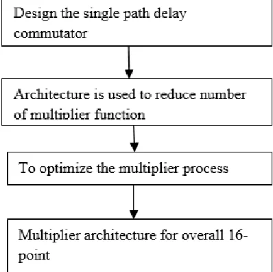
The existing system is to design the pipelined radix-2 based FFT architecture. This architecture is to consists of more no of multiplier architecture, so it affect the system performance level. The existing radix process is to modify the butterfly level for 16-point architecture and to implement the carry save adder architecture for multiplier adder section. The existing architecture is to analysis overall path delay for the real and complex multiplier system process. The existing system is a single path delay commutator – feed-back based FFT architecture and this work is to optimize the number of multiplier count level. Existing system is to identify the critical path section for overall 16-point radix-2 FFT architecture and to analysis weighted section for multiplier process. Existing system is to consists of bit reversal, adder/subtractor, and real multiplier and register architecture and to reduce the overall logical gate for proposed method.
Today’s electronic systems mostly run on batteries thus making the designs to be hardware efficient and power efficient. Application areas such as digital signal processing, communications, etc. employ digital systems which carryout complex functionalities. Hardware efficient and power efficient architectures for these systems are most required to achieve maximum performance. Fast Fourier Transform (FFT) is one of the most efficient ways to implement Discrete Fourier Transform (DFT) due to its reduced usage of arithmetic units. DFT is one of those primary tools that are used for the frequency analysis of discrete time signals and to represent a discrete time sequence in frequency domain using its spectrum samples.
The SDC PE consists of a data commutator, a real add/sub unit, and an optimum complex multiplier unit. In order to minimize the arithmetic resource of the SDC PE, the most significant factor is to maximize the arithmetic resource utilization via reordering the data sequences of the above three units. In the stage t, the data commutator shuffles its input data (Node−A) to generate a new data sequence (Node−B), whose index difference is N/2t, where t is the index of stage.
We propose a novel pipelined FFT architecture which produces the output data in normal order. Using the proposed combined single-path delay commutator (SDC) and single-delay feedback(SDF), the new pipelined architecture achieves 100% hardware utilization In order to produce the output sequence in normal order, a bit reverser saving 50% of memory requirement is proposed. Compared with the conventional pipelined FFT designs, the proposed architecture reduces the number of adders, multiplier s and hardware implementation complexity. Therefore, the proposed FFT architecture is suitable for the implementation of pipelined FFT processors with the input and output sequence in normal order. The SDF architecture does not meet the above constraint well since the sums of the all butterflies in the stage are produced first, followed by the corresponding differences. A novel pipelined FFT architecture which produces the output data in normal order.
In addition to this, the designs can achieve very high through puts, which makes them suitable for the most demanding applications. Indeed, the proposed radix-2 k Feed forward architectures require fewer hardware resources than parallel feedback ones, also called Multi-path Delay Feedback (MDF), when several samples in parallel must be processed. As a result, the proposed radix-2 k Feed forward architectures not only offer an attractive solution for current applications, but also open up a new research line on feed forward structures.
III. PROPOSED WORK
In proposed system a ADAPTIVE SPLIT variable length based 16-point FFT architecture is developed. This architecture reduce the register and bit reviser element. This Adaptive Split design transform process maintain the self optimizing approach and to implement the high performance based arithmetic operator architecture. These architectures perform the real and complex binary operation in 16-Point FFT adder, subtractor, parallel multiplier section. Then to increase the data rate for FFT transform function and to analysis the critical path functional level. Finally to improve the weighted section performance level and to improve the constant multiplier functional level.
However, some of the rotators in radix-2 3 and radix-2 4 FFTs can be simplified, as they only have to calculate rotations by W8 and W16. Compared to previous radix-2 4 parallel feedback architectures, the proposed radix-2 4 designs save 50% of the adders and reduce the memory requirements, while having the same number of rotators[10]. As regards 4-parallel architectures, the proposed radix-2 2 feed forward FFT and the radix-4 feed forward FFT [3] require the lowest number of rotators, adders and memory among all the designs in the literature. Although radix-2 2 and radix-4 architectures require the same total number of hardware resources for 4-parallel samples, the layout of these resources is different[8][5]. This FPGA includes DSP48E blocks that can be used to carry out mathematical operations. The fast Fourier transform (FFT) is one of the most important algorithms in the field of digital signal processing. It is used to calculate the discrete Fourier transform (DFT) efficiently. There are two main types of pipelined architectures: feedback (FB) and feed forward (FF)[2]. On the one hand, feedback architectures are characterized by their feedback loops, i.e., some outputs of the butterflies are fed back to the memories at the same stage.
Applications of proposed system:
1) Digital signal processing applications. 2) MIMO-OFDM channel process. 3) Biometric Solution.
4) Forensic applications
The forensic application is nothing but the analysis of DNA sequences. It can be used in the medical field.
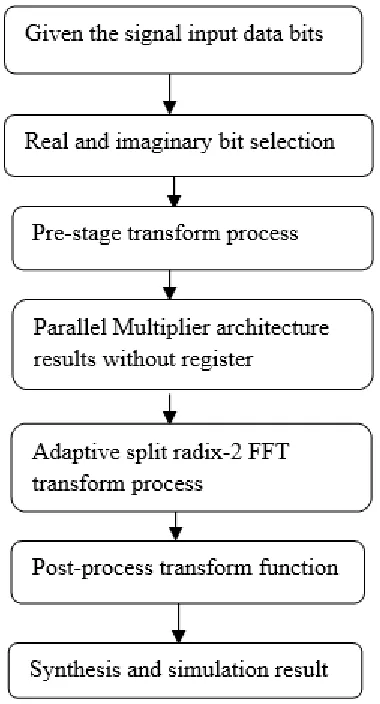
Proposed Architecture Diagram
Fig. 1: Proposed Architecture diagram
First select real and imaginary bits and add and subtract real and imaginary bit values. Then to update weighted value for required stage cycle for overall FFT architecture. The weight equation is to set 0 to 15 position level [1] and to obtain the 16-point radix -2 based FFT architecture. This section include the carry select adder and subtractor architecture for pre-stage operation. This section is to reduce the path delay complexity level. Finally, the architecture can be simulated.
Class diagram of Proposed System
Our FFT architecture consists the 4-bit, 8-bit, 16-bit adder and subtractor architecture. These architecture is used to process the frequency domain based digital transformation function. A basic full adder/half adder/ full subtractor/ half subtractor has three inputs and two outputs which are sum and carry. These logic circuits of this full adder can be implemented with the help of XOR gate, AND gates, NOT gates and OR gates. The XOR gate is the basic building block of the these type of addition and subtraction circuit.
Fig. 2: Class diagram
Adaptive Split Radix-2 Transform Design
We design a 16-point adaptive split radix-2 FFT architecture. This architecture reduces the register element and improve the arithmetic operation architecture. This design is to enhance the real and imaginary data transform process circuit complexity and process time delay level. An Adaptive Split FFT architecture is a way to compute the same result more quickly. Our ADAPTIVE FFT algorithms are also much more accurate than evaluating the DFT architecture.
Fig. 3: Aspects of Adaptive split FFT
Weight Update Unit
The weight update level is followed in equation of,
WNK = e(-j2πk/N)
These values are multiplied in single path transformation bit values and to generate the real multiplier section level. Our design is to develop a parallel multiplier architecture for weighted multiplication section level.
IV. RESULTS
Justification of Results
First we design a 16-point FFT architecture internal component. This structure consists of adder, subtractor, and multiplier architecture. So we focus the more no of arithmetic operator present in our proposed architecture. We design and modify the adder, subtractor component architecture using carry look ahead technique. Finally we design a efficient vlsi based ADAPTIVE SPLIT variable length based radix-2 FFT architecture and to optimize the circuit complexity level compare to the existing architecture. Finally we simulate and synthesis overall final FFT architecture and compare to existing methodology.
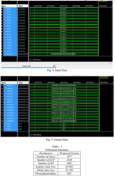
Fig. 4: Input Data
Fig. 5: Output Data
Table - 1 Utilization Summary Parameters Proposed System Number of slices 877
Number of LUT 1548 Number of IO 640 Latency time (ns) 53.965
Delay time (ns) 23.106 Throughput(mbps) 692
Power(mw) 811
Throughput Calculation
The throughput can be given as the ratio of number of data transmitted and the delay time. In proposed system, the throughput can be calculated as follows,
Throughput = Number of data transmitted / Delay Time = 16/23.106
= 0.6924 = 692Mbps
Comparison of Performance
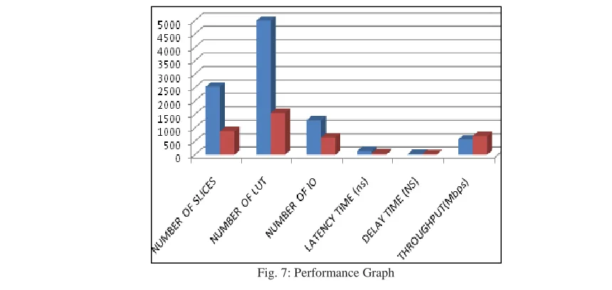
Table - 2 Comparison Table
Existing systems Proposed system
Parameters Pipelined feed forward FFT architecture (2015)
Multi-path delay commutator Architecture (2014)
Adaptive Split Radix-2 FFT architecture
NUMBER OF SLICES 2532 - 877
NUMBER OF LUT 4992 - 1548
NUMBER OF IO 1280 - 640
LATENCY TIME (ns) 140 - 53.965
POWER (mW) 858 - 811
THROUGHPUT(Mbps) 568 - 692
DELAY TIME (NS) - 28.162 23.106
Here, the tables shows the comparison performance of proposed system. The delay time and power can be highly reduced compare to the existing system. Data transmission speed can be highly optimized in our proposed system. The throughput calculation shown above can be done based on the data transmission and delay time and it will be increased compared to the existing system.
Fig. 7: Performance Graph
V. CONCLUSION AND FUTURE WORK
Finally, we design a efficient VLSI based Adaptive Split variable length based radix-2 FFT architecture and optimize the circuit complexity level compare to the existing architecture. In this system, the power can be reduced to 811mW and Data speed can be increased to 692Mbps compare to existing system. Our Future work is to optimize the parallel multiplier architecture level and to implement the VEDIC multiplier architecture for constant multiplication process. This architecture reduces the FFT architecture complexity level and to increase the transformation speed level and the architecture can be developing for 16 bits.
REFERENCES
[1] Cheng .C and Parhi K. K. “High throughput VLSI architecture for FFT computation,” IEEE Trans. Circuits Syst. II, Exp. Briefs, vol. 54, no. 10, pp. 339– 344, Oct. 2007.
[2] Cortes A, Velez.I, and Sevillano J.F, “RadixRKFFTs: Matricial representation and SDC/SDF pipeline implementation,” IEEE Trans. Signal Process., vol. 57, no. 7, pp. 2824–2839, Jul. 2009.
[3] Cho T, Tsai S, and Lee H, “A high-speed low-complexity modified radix-25 FFT processor for high rate WPAN applications,” IEEE Trans. Very Large Scale Inegr. (VLSI) Syst., vol. 21, no. 1, pp. 187–191, Jan. 2013.
[4] Garrido M, Grajal J, Sanchez M, and Gustafsson “Pipelined radix-2k feedforward FFT architectures,” IEEE Trans. Very Large Scale Inegr. (VLSI) Syst., vol. 21, no. 1, pp. 23–32, Jan. 2013.
[5] Liu X,Yu F, and Wang Z.K, “A pipelined architecture for normal I/O order FFT,” J. Zhejiang Univ. Sci. C, vol. 12, no. 1, pp. 76–82, Jan. 2011.
[6] LinY.W,. LiuH.Y, andLeeC.Y,“A1GS/sFFT/IFFTprocessor for UWB applications,” IEEE J. Solid-State Circuits, vol. 40, no. 8, pp. 1726–1735, Aug. 2005. [7] Narmadha. G and Deivasigamani. S,” An Efficient Multipath delay commutator architecture”, International journal of computer application,
July2014,vol.98,pp.21-23.
[8] Oh J.h and Lim M.S, “Area and power efficient pipeline FFT algorithm,” inProc. IEEE Workshop Signal Process. Syst. Design and Implementation, Nov. 2005, pp. 520–525.
[9] Rabiner L. R. and Gold B, Theory and Application of Digital Signal Processing. Englewood Cliffs, NJ, USA: Prentice-Hall,Nov. 2003, pp. 604–609. [10] Shin M. and Lee H., “A high-speed, four-parallel radix-2 4 FFT processor for UWB applications,” inProc. IEEE ISCAS, May 2008, pp. 960–963. [11] Zeke Wang, Xue Liu, Bingsheng He, and Feng Yu, “A Combined SDC-SDF Architecture for Normal I/O Pipelined Radix-2 FFT”, IEEE transaction on VLSI