e-ISSN: 2250-3021, p-ISSN: 2278-8719 Vol. 3, Issue 4 (April. 2013), ||V1 || PP 17-26
Simulation Aspects of Thyristor Controlled Series
Compensator in Power System
Kusum Arora
1, S.K. Agarwal
2, Narendra kumar
3, Dharam Vir
41, 2&4
YMCA University of Science & Technology, Faridabad, Haryana 3
Delhi Technological University, New Delhi
Abstract : The Thyristor controlled series compensator (TCSC) is one of the important members of FACTS
family that is increasingly applied with long transmission lines by the utilities in modern power systems. It can have various roles in the operation and control of power systems, such as scheduling power flow; decreasing unsymmetrical components; reducing net loss; providing voltage support; limiting short-circuit currents; mitigating sub synchronous resonance; damping the power oscillation and enhancing transient stability control of power systems, systems and procedures are used to compensate dynamically the detrimental effect of nonlinear loads. The compensation process should be carried out without important alteration of the signal quality along with some benefits like reduction of losses in distribution lines, harmonic content minimization and power factor improvement. The dynamic behavior of industrial load requires the use of that compensator which can be adapted to the load changes. Thyristor Controlled Series Capacitor (TCSC) is an important FACTS device which has been used in power system transmission networks; these few aspects of the TCSC operation which we are simulating in ORCAD and MATLAB (i) To calculate the various resonance points in the impedance characteristics of the TCSC w.r.t. various firing angle. (ii) Contribution of the TCSC to power system operation and control system and study by implementing the TCSC in small power model of power system using ORCAD and MATLAB.
Keywords: FACTS, Series Compensator, TCSC, Thyristor, MATLAB.
I. INTRODUCTION
Power electronic devices, such as high voltage dc converters and static var compensators, have long established their usefulness in bulk power transmission. The scope of application of such devices has been extended considerably in recent years, as these devices provide much better transient responses, compared with their mechanical, electrical and electromechanical counterparts. The use of any such device can increase the level of power that can be transferred over a transmission corridor without endangering the system stability [1] [9]. Thyristor-controlled series capacitors (TCSC) is a type of series compensator, can provide many benefits for a power system including controlling power flow in the line, damping power oscillations, and mitigating sub synchronous resonance. Shunt compensation is ineffective in controlling the actual transmitted power as given by [2]:
S R s
Z V V
P sin
Where Zs=Series Line Impedance, δ = Angle between the end voltages, P=Actual transmitted power, Vs= Sending end voltage, Vr= Receiving end Voltage
The variable series compensation is highly effective in both controlling power flow in line and improving stability, design, model and implement the TCSC in power system model is simulations are performed using the MATLAB. The rest of the paper is as organized section 2 Literature survey Section 3 TCSC model considering Section 4 Analysis of TCSC section 5 Experimental setup and response of the zero cross detector, response of the A/D converter, and firing pulses of the SCR i.e. output of the microcontroller, simulation analysis of the implemented TCSC circuit section 6 consists of conclusion and further scope of work.
II. LITERATURE SURVEY
Hailian Xie and Lennart Angquist designed a new control scheme instead of traditional firing angle control scheme called as the Static Voltage Reversal Control scheme. Following that scheme the simulation results are analyzed using real time simulator [3].
Dragan Jovcic, member IEEE and G.N.Pillai presents an analytical, linear, state-space model of TCSC. First a simplified fundamental frequency model of TCSC is proposed and the model results are verified. Using the nonlinear TCSC segment, a simplified nonlinear state space model is derived where frequency of dominant TCSC complex poles shows linear dependence on the firing angle. The nonlinear element is linearised and linked with the AC network model along with TCSC model and is implemented on MATLAB and verified on EMTDC/ PSCAD in frequency and Time domain for a range of operating conditions [5] [18].
T.Vengas and C.R. Fuerte-Esquivel develop a steady-state mathematical model of the new generation of power electronic based plant component presently emerging as a result of FACTS devices. Modeling is done in the phase domain considering the TCSC physical nature. A poly-phase power flow program based on Newton algorithm is developed in order to implement the proposed model [17].
III. TCSC MODEL CONSIDERING
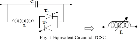
This device has been traditionally modeled as a thyristor-controlled reactor in parallel with a fixed capacitor; the reactor and capacitor are represented only by their corresponding reactance.
Fig. 1 Equivalent Circuit of TCSC
3.1 Modes of operation of TCSC
There are three modes of operation of TCSC depending upon the firing angle of the pulses fed to the thyristor [8].
Thyristor blocked mode
Thyristor by passed mode
Vernier operating mode
3.1.1 Thyristor blocked Operating Mode:
When the thyristor valve is not triggered and the thyristors are kept in non conducting state, the TCSC is operating in blocking mode. In this mode, the TCSC performs like a fixed series capacitor.
3.1.2 Thyristor bypass Operating mode:
In bypass mode the thyristor valve is triggered continuously and the valve stays conducting all the time; so the TCSC behaves like a parallel connection of the series capacitor with the inductor, Ls in the thyristor valve branch. In this mode, the resulting voltage in the steady state across the TCSC is inductive and the valve current is somewhat bigger than the line current due to the current generation in the capacitor bank. For practical TCSC’s with ratio (XL/XC) between 0.1 to 0.3 ranges, the capacitor voltage at a given line current is much lower in bypass than in blocking mode. Therefore, the bypass mode is utilized as a means to reduce the capacitor stress during faults [6] [15].
3.1.3 Vernier Operating Mode:
In Vernier control the TCSC dynamics are varied continuously by controlling the firing angle. The firing angle is possible from 0o to 90o for each half cycle when it is generated from the zero crossing of the line current hence divided into two parts [8] [10];
Capacitive Boost mode: In capacitive boost mode a trigger pulse is supplied to the thyristor having forward
Inductive Boost Mode: In inductive boost mode the circulating current in the TCSC thyristor branch is bigger than the line current. In this mode, large thyristor currents result and further the capacitor voltage waveform is very much distorted from its sinusoidal shape. The peak voltage appears close to the turn on. The poor waveform and the high valve stress make the inductive boost mode less attractive for steady state operation. This mode increases the inductance of the line, so it is in contrast to the advantages associated with the application of TCSC [7] [19].
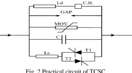
3.2 Practical TCSC circuit:
Practical TCSC circuit has various protection elements including MOV, circuit breaker in series with an inductor. TCSC module with different protective elements is as shown below.
Fig. 2 Practical circuit of TCSC
Basically, it comprises a series capacitor, in parallel with a Thyristor Controlled Reactor (TCR), Ls. A Metal Oxide Varistor (MOV), essentially a nonlinear resistor, is connected across the series capacitor to prevent the occurrence of high capacitor over voltages. Not only does the MOV limit the voltage across the capacitor, but it allows the capacitor to remain in the circuit even during fault conditions and helps improve the transient stability. A circuit breaker is also installed across the TCSC module to bypass it if a severe fault or equipment malfunction occurs. A current limiting inductor, Ld is incorporated in the circuit to restrict both the magnitude and the frequency of the capacitor current during the capacitor bypass operation [11] [13].
IV. TCSC IMPLEMENTATION ON HARDWARE
4.1 Design of Power circuit:
The power circuit of TCSC is designed with the small model of the power system .The main power supply is treated as the transmitting end generator’s output with zero phase angle and 220 volts rms .From transformers secondary we can get twelve volts output to regulate it to +5 volts using center tapped full wave rectifier and regulator 7805 which is required for energizing zero cross detector, for the Vcc of microcontroller, for biasing of the transistor used as drivers and for opto-isolator but here we used it only for the opto isolator circuit and for other circuit another transformer is being used [14].
4.2 Design of Transmission line model:
Further after the generator there exists the transmission lines and here transmission lines are replaced by their pre calculated values of line inductance and resistances .Here value of line inductor assumed is 14mH and value of resistance is 4ohms.After transmission line TCSC is implemented in the middle of the circuit and again at the receiving end there is transmission line of the same rating. Resistances are taken with minimum of 5W power rating and inductors are designed in the lab by own [12].
4.3 Design of Inductors:
The inductor is designed around the soft ferrite E core. Soft ferrite core can operate in the power range of 200W-500W at a frequency of 100KHz.Two E cores are joined together with an air gap between the legs. Use of a gapped core can reduce the effect of permeability and result in high saturation level because the air gap can withstand much higher field strengths. Insulated copper wire is wound around the inner legs of the core. The inductance is directly proportional to the square of the number of turns of the winding and corresponding area of the core and inversely proportional to the length of the air gap as given below [15]:
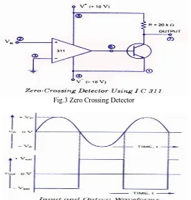
4.4 Zero crossing detector circuit:
edge of the square wave. This rising edge will occur after every ten milliseconds for a line frequency of 50Hz. In this way α is generated by delaying the trigger pulses to thyristor firing pulses [16].
Here the firing pulses of the power semiconductor devices are synchronized with the line voltage because such procedure reduces the signals harmonic content .Therefore, a signal whose waveform coincides with that of the line voltage is required.
Fig.3 Zero Crossing Detector
Fig. 4 Output waveform of the zero cross detector:
4.5 TCSC Hardware Implementation:
Fig. 5 Hardware implementation of TCSC
and pasting it in the shape of former. After getting wound value of the inductance is measured on the inductance meter and if there were any ups or downs the no of turns were decreased or increased accordingly. Similar way other inductors were designed. Similarly capacitance and load resistance and load inductance is estimated. In this case the estimated parameters are Rt=0.01ohms; Ct=500uF; L-load=5mH; R-load=15ohm.
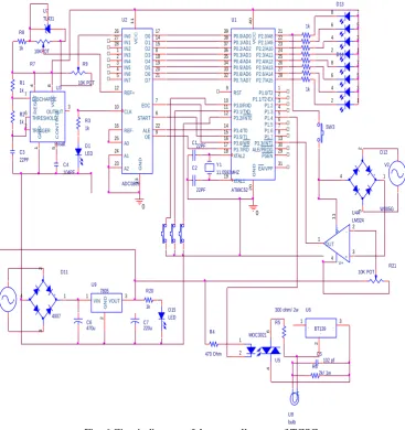
4.6 Microcontroller based control circuit:
In this stage an 89C52 microcontroller is used. The microcontrollers detects the zero crossings of the square signal coming out of the signal conditioning stage, and delivers a firing pulse with a delay time proportional to the desired firing angle using even input bits. Each thyristor has a separate pulse and the firing angle has an accuracy of one electrical degree. The input port of the microcontroller is set for the condition of zero cross detector and the required delay is fed through the helical potentiometer through which analog I/P is given and the microcontroller inside A/D converter will convert those analog output into digital and hence delay is defined w.r.t. the high level of zero cross detector .The output port of Microcontroller will provide the trigger pulse only if zero cross detector o/p is high and the delay is defined w.r.t. the high output of the zero cross detector. Fig 6.
Fig. 6 Circuit diagram of the controller part of TCSC
The input port of the microcontroller is set for the condition of zero cross detector and the required delay is fed through the helical potentiometer through which analog I/P is given and the microcontroller inside A/D converter will convert those analog input into digital and hence delay is defined w.r.t. the high level of zero cross detector .The output port of Microcontroller will provide the trigger pulse only if zero cross detector o/p is high and the delay is defined w.r.t. the high output of the ZCD [20].
V. SIMULATION OF TCSC FOR SINGLE RESONANT POINT
U1 AT89C52 RST 9 XTAL2 18 XTAL1 19 GN D 20 PSEN 29 ALE/PROG 30 EA/VPP 31 VC C 40 P1.0/T2 1 P1.1/T2-EX 2 P1.2 3 P1.3 4 P1.4 5 P1.5 6 P1.6 7 P1.7 8 P2.0/A8 21 P2.1/A9 22 P2.2/A10 23 P2.3/A11 24 P2.4/A12 25 P2.5/A13 26 P2.6/A14 27 P2.7/A15 28 P3.0/RXD 10 P3.1/TXD 11 P3.2/INT0 12 P3.3/INT1 13 P3.4/T0 14 P3.5/T1 15 P3.6/WR 16 P3.7/RD 17 P0.0/AD0 39 P0.1/AD1 38 P0.2/AD2 37 P0.3/AD3 36 P0.4/AD4 35 P0.5/AD5 34 P0.6/AD6 33 P0.7/AD7 32 U2 ADC0809 CLK 10 OE 9 EOC 7 D0 17 D1 14 D2 15 D3 8 D4 18 D5 19 D6 20 D7 21 START 6 ALE 22 VC C 11 GN D 13 REF+ 12 REF-16 IN0 26 IN1 27 IN2 28 IN3 1 IN4 2 IN5 3 IN6 4 IN7 5 A0 25 A1 24 A2 23 U3 555alt GN D 1 TRIGGER 2 OUTPUT 3 R ESET 4 C ON T R OL 5 THRESHOLD 6 DISCHARGE 7 VC C 8 U4A LM324 + 3 - 2 V+ 4 V-11 OUT 1 U5 MOC3021 1 2 6 4 D13 7 8 5 6 4 2 3 1 Y1 11.0592MHZ D14 7 8 5 6 4 2 3 1 C122PF C2 22PF 0 R1 1k R2 1k R3 1k C3 22PF C4 104PF D1 LED SW3 R21 10K POT U6 BT139 . 1 . 3 . 2 R4 470 Ohm R5 300 ohm/ 2w
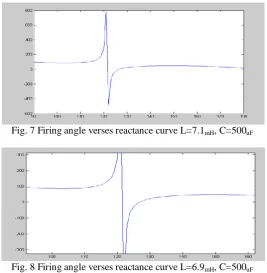
5.1 Impedance Characteristics Curve:
With the given parameters of a TCSC, the steady-state mapping relationship between the firing angle and fundamental frequency reactance can be analyzed by writing the equation for the given TCSC circuit in the m.file of the MATLAB [17] [18] .These programs are written in simple language. Relationship between reactance and firing angle is different for the various values of the inductance and capacitance and also resonant points may be one or more depending upon the various values of capacitor inductance combination. If the frequency of supply is 50Hz then for a given values of capacitor=500uf and inductor=7.1mH as taken in the provided software and hardware circuit, also one reference example is also considered for the evaluation of its reactance this circuit used in Kayanta substation in USA having inductance value 6.9mH and capacitance of 177uF we can have various frequency responses
Fig. 7 Firing angle verses reactance curve L=7.1mH, C=500uF
Fig. 8 Firing angle verses reactance curve L=6.9mH, C=500uF
5.2 Various parameters of TCSC circuit:
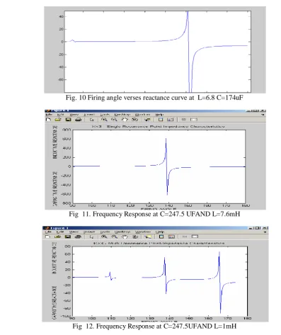
If the equation used is as given above , where instead of firing angle ,conduction angle is used in the calculation and parameters are also according to one of the places where TCSC is really installed and frequency of the power system is also 60 Hz. Simulation response of this equation written above is as given below:
Fig. 9 Firing angle verses reactance curve at L=6.85mH,C=174uF
Fig. 10 Firing angle verses reactance curve at L=6.8 C=174uF
Fig 11. Frequency Response at C=247.5 UFAND L=7.6mH
Fig 12. Frequency Response at C=247.5UFAND L=1mH
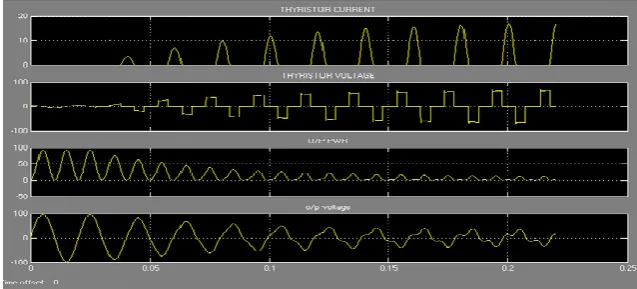
response of the TCSC to demanded change in from 1 p.u. to 2.1p.u., corresponding to a change in firing angle from to 175o to151o. It can be seen from scope output that more than 200 ms is needed for the fundamental frequency reactance to reach its new steady-state value. Simulation results of the TCSC model with pulsar having phase delay of 5.2ms=91.2o will give the results as shown below. As shown below it takes almost 200ms or we can say about five complete cycles for fundamental frequency to reach its new steady state value.
Fig. 13 shows Thyristor current, Thyristor voltage, Thyristor output power and output voltage.
5.3 Simulink Model of TCSC:
Fig. 14 shows the Simulink Model of TCSC
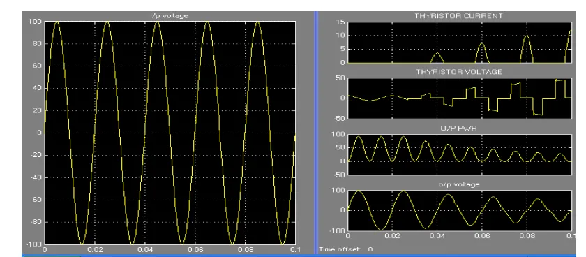
5.4 Simulation Results of TCSC:
Fig. 16 Simulation results shows of output Thyristor current, Thyristor voltage, o/p power, o/p voltage when Delay of pulser1=0.0175s and delay of pulser2=0.0275s i.e. α=125o and 300o
Transient response of TCSC is analyzed by increasing the simulation time. The response got stable after few seconds of the firing as shown above.
VI. CONCLUSION AND FUTURE SCOPE OF WORK
Similarly in future implementation could be of a three-phase device as well as the evolution to series compensation may be by voltage sourced converters it can also be implemented with Neuro and fuzzy logic or some different strategies may now be developed to control the reactance of the TCSC through firing angle adjustments.
REFERENCES
[1]. Y.H. Song, “Flexible AC Transmission Systems (FACTS)”, the Institution of Electrical Engineers, London, 1999.
[2]. H.F. Wang, F.J. Swift, “A unified model of FACTS devices in damping power system oscillations
part-1”: single-machine infinite-bus power systems, IEEE.
[3]. Sidhartha Panda, N.P. Padhy, Comparison of particle swarm optimization and genetic algorithm for FACTS-based controller design, Appl. Soft Computing.
[4]. N.G. Hingorani and L. Gyugyi “Understanding FACTS Concept and Technology of Flexible AC
Transmission Systems”,IEEE Press.
[5]. N.Christl, R.Heddin, K.Sadek, Plutzelbergger (Siemens AG) – Germany & P.E. Krause, S.M.McKenna, A.H.Montoya , D.Torgerson (United States) – United States “Advanced Series Compensation(ASC) with Thyristor Controlled Impedance”, CIGRE 3.5 Rue De Metz 75010 Paris – 14/37/38-05.
[6]. T.Vijayakumar, A. Nirmalkumar and N.S.Sakthivelmurugan – Implementation of FC – TCR using Low Cost 89c2051 Controller- Research Journal of Applied Sciences, Engineering & Technology 1(2) 40-43, 2009.
[7]. Pavel Zuniga Haro, Student Member, IEEE and Juan Manuel Ramirez Arredondo, Member,IEEE - “Experimental results on a Lab Scale Single Phase TCSC” – 0-7803-7519-X/02, 2002 IEEE.
[8]. Mojtaba Noroozian, Senior Member IEEE, Mehrdad Ghandhari,Student Member , IEEE, Goran Andersson, Fellow,IEEE, J.Gronquist, Member IEEE and I.Hiskins,Senior Member IEEE – “A robust control strategy for Shunt and Series Reactive Compensators to Damp Electronmechanical Oscillations – 0885-8977 /2001 IEEE.
[9]. Jonas Persson, Lennart Soder , Stockholm, Swedan – “Validity of a Linear Model of a Thyristor Controlled Series Capacitor for Dynamic Simulations” – 14th PSCC, Sevilla, 24-28 June 2002
[10]. John Persson, Student Member IEEE, Luis Rouco and Lennart Soder, Member IEEE – “Linear Analysis
with Two Linear Models of a Thyristor Controlled Series Capacitor” – IEEE Bologna Power Tech Conference on June 23rd-26th, Italy – 0-7803-7967-5/03/ 2003 IEEE.
[11]. Preeti Singh, Mrs.Lini Mathew, Prof.S.Chatterji, NITTTR, Chandigarh “Matlab based Simulation of
TCSC FACTS Controller” – 2ND National Conference on Challenges & Opportunities in Information
Technology (COIT-2008) - March 2008.
[12]. N.Magaji, M.W.Mustafa ,University Technology, Malaysia ON “Optimal Thyristor Control Series
Capacitor Neuro-Controller for Damping Oscillations” Journal of Computer Science 5 (12) :983-990, 2009 ISSN 1549-3636.
[13]. K.Vijayakumar and R.P.Kumudini Devi, Anna University, Tamilnadu ON “A Hybrid Genetic Algorithm
for Optimal Power Flow Incorporating FACTS devices” – Asian Journal of Scientific Research 1(4): 403-411,2008 ISSN 1992:1454.
[14]. G.Escobar, A.M.Stankovic- USA, P.Mattavelli-Italy, R.Ortega-France ON “On the nonlinear control of
TCSC” – 0-7695-1435-9/ 2002 IEEE.
[15]. B.H.Li, Q.H.Wu, Senior Member IEEE, P.Y.Wang, X.X.Zhou, Fellow IEEE ON “Influence of the
Transient Process Process of TCSC and MOV on Power System Stability –IEEE Transactions on Power Systems, Vol:15, No; 2, May 2000.
[16]. T.Venegas, C.R.Fuerte – Esquivel ON “Steady State Modeling of TCSC for phase domain load flow analysis of Electrical Networks” 0-7803-5902-x/ 2000 IEEE.
[17]. Mojtaba Khederzadeh and Tarlochan Singh Sidhu, Fellow IEEE ON “Impact of TCSC on the Protection
of Transmission Lines” – IEEE Transactions on Power Delivery, Vol: 21, No: 1, January 2006.
[18]. S.Meikadasivam, Rajesh Kumar Nema, Shailendra Kumar Jain ON “Behavioral Study of TCSC Device –
A Matlab/ Simulink Implementation”- World Academy of Science, Engineering and Tech. 45 – 2008.
[19]. Alireza Daneshpooy,A.M. Gole “Frequency Response Of The Thyristor Controlled Series Capacitor”
IEEE TRANSACTION ON POWER DELIEVERY,VOL.16 ,NO.1,JANUARY 2001.
[20]. X.D.Liu, Y.X.Ni, C. Chen (S.M. IEEE) and Felix F. Wu (Fellow IEEE) ON “Bifurcation Phenomenon of