IMPLEMENTATION OF DIGITAL
FILTERS FOR HIGH THROUGHPUT
APPLICATIONS ON FPGA
T.PUSHPA
Asst.professor., Vignana bharathi institute of technology,Hyderabad,AP,India, [email protected]
M.VENKATLAKSHMI
Asst.professor,Vignana bharathi institute of technology,Hyderabad,AP,India, Email: [email protected]
Abstract:
The digital filter implementation in FPGA,utilising the dedicated hardware resources can effectively achieve ASIC-like performance while reducing development time cost and risks. Advantage of FPGA approach to digital filter implementation including sampling rates than are availablefrom traditional DSP chips. In this paper a low pass,band pass and highpass FIR filter is implemented on FPGA.This approach gives a better performance than the common filter structures in terms of speed of operation,cost and power consumption in real time.In this technique, codes for direct fixed point FIR filter have been realized. Modules such as multiplier, adder, ram and two’s complement were used. For an N order filter the filter the number of registers and adders required is N and the number of multipliers required is N+1.For high speed and high throughput applications,MAC is used and that consumes less power.
Keywords: Filters, MAC, DA algorithm and FPGA. 1. Introduction
The finite impulse response(FIR) filter is a digital filter widely used in digital signal processing applications in various fields like imaging, instrumentation, communications etc. Programmable digital signal processors (pdsps) can be used in implementing the fir filter. However,in realizing a large-order filter many complex computations are needed which affects the performance of the common digital processors in terms of speed,cost,flexibility etc. FPGA has become an extremely cost-effective means of off-loading computationally intensive digital signal processing algorithms to improve overall performance. In real time signal processing requires high speed and high throughput Multiplier-Accumulator(MAC) unit that consumes low power,which is always a key to achieve high performance DSP system.The purpose of this work is to design and implementation of low power geometrics that give optimized power, area and delay.This paper presents methods of implementing high speed binary multiplication and distributed arithmetic is well suited for LUT based FPGA architectures.Which make the memory size smaller and minimizing the latency, with the goal being the implementation of the fastest multiplication blocks possible.
2. Multiplier and Accumulation
In general, a multiplier uses Booth’s algorithm and array of full adders (FAs), or Wallace tree instead of the array of FA’s., i.e., this multiplier mainly consists of the three parts: Booth encoder, a tree to compress the partial products such as Wallace tree, and final adder. Because Wallace tree is to add the partial products from encoder as parallel as possible, its operation time is proportional to, where is the number of inputs. It uses the fact that counting the number of 1’s among the inputs reduces the number of outputs into. In real implementation, many (3:2) or (7:3) counters are used to reduce the number of outputs in each pipeline step: 2.1 Overview Of MAC
Fig: 2.1 Basic arithmetic steps of multiplication and accumulation
The Basic arithmetic steps of multiplication and accumulation is shown in Fig. 2.1. The last is the final addition in which the process to accumulate the multiplied results is included.
3. Distributed Algorithm
Distributed Arithmetic (DA) algorithm appeared as a very efficient solution especially suited for LUT-based FPGA architectures. Croisieretal had proposed the multiplier less architecture of DA algorithm and it is based on an efficient partition of the function in partial terms using 2’s complement binary representation of data. The partial terms can be pre-computed and stored in LUTs. Yoo et al. [8] observed that the requirement of memory/LUT capacity increases exponentially with the order of the filter, given that DA implementations need 2K – words, K being the number of taps of the filter.
3.1 Distributed Arithmetic (DA) The FIR digital filter is presented as:
(1)
Where y[n] is the FIR filter output, x[n − k] is input data and c[k] represents the filter coefficients Equation(1) shows that multiplier-based filter implementations may become highly expensive in terms of area and speed.
Distributed arithmetic (DA) is an important FPGA technology. It is extensively used in computing the sum of products
( 2) DA system, assumes that the variable x[n] is represented by-
( 3) If c[n] are the known coefficients of the FIR filter, then output of FIR filter in bit level form is:
(4)
In distributed arithmetic form (5) In Equation (5) second summation term realizing as one LUT. The use of this LUT or ROM eliminates the multipliers [9]. For signed 2’s complement number output of FIR filter can be computed as-
(6) Where B represents the total number of bits used. Fig 2.1 shows the Distributed architecture for FIR filter and different with the MAC architecture. When x[n] <0, Binary representation of the input is [10],
( 8)
If the number of coefficients N is too large to implement the full word with a single LUT (Input LUT bit width = number of coefficients), then partial tables can be and add the results as shown in Fig 4.2. If pipeline registers are also added, then this modification will not reduce the speed, but can dramatically reduce the size of the design.
3.2 Parallel distributed arithmetic Architecture
A basic DA architecture, for a length nthsum-of-product computation, accepts one bit from each of N words. If two bits per word are accepted, then the computational speed can be essentially improved. The maximum speed can be achieved with the fully pipelined word-parallel architecture. For maximum speed, a separate ROM (with identical content) for each bit vector xb[n] should be provided
Numerical example: Input
Integer binary multiplication
7 0111 7*2^0+1=8 3 0011 3*2^1+8=14
1 0001 1*2^2+14=18
Proposed Method
Memory efficiency when "000" => 0; when "001"=> 2; when "010"=> 3; when "011"=> 5; when "100"=> 1; when "101"=> 3; when "110" => 4; when "111" => 6;
integer binary
7 111
3 011
1 001
P0=0 Iteration 1
P1= (P0/2)*(memory*4)=p1=[(0/2)+(2*4)]=8 Iteration 2
8
2
(5 * 4)
24
2
p
Iteration 3
24
3
(6 * 4)
18
2
p
1
0
0
1
1
0
1
1
1
4. Implementation: 4.1 Design procedure
Step1: Derive the filter coefficient according to specification of filter. Step2: Store the inputs value in input register.
Step3: Design the LUTs as which represents all the possible sum combination of filter coefficients.
Step4: Accumulate and shift the value according to partial term beginning with LSB of the input and shift it to the right to add it to the next partial result.
Step5: First value must be subtracted, due to negative bit of MSB.
Step6: Analyze the output of filter as per specifications, otherwise go to step 1.
Step7: The same procedure is applied for Parallel DA FIR from step 1 to step 6 except in Step3
where bit address value is being called for 2-bits at single time, so that two times LUT is required in comparison to the serial DA.
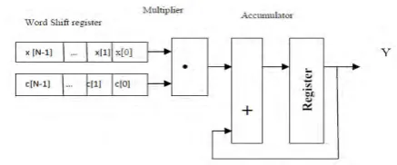
Fig 4.1 Distributed architecture for FIR filter with MAC architecture.
4.2 Implementation:
High Level Specifications are nothing but the requirements to understand and begin the design. In this stage the designer main aim is to capture the behavior of the design using mostly behavioral constructs of the HDL’s. The next step after capturing the designs functionality is to segregate the design in all possible ways and try to write a synthesizable code which infers available primitives from the library.
Here mostly the mixed style of modeling is used and only synthesizable constructs of the HDL is used. Then comes the synthesis step which is actually target driven. Here we have an FPGA as the target device. Then Implementation is nothing but the process of placing and routing the design on an FPGA. Mostly it is a tool driven and no manual intervention of the designer is required. Designer only needs to specify constrain file in design if any.
5. Simulation Results Iteration 1
Iteration 3
Wallace Tree
Da Algorithm
6. Conclusion:
DA algorithm which is implemented consumes low power of 0.10 watts when compared with recent implementation like Wallace tree which consumes 0.30 watts power .An achievement of 0.20 watts power has been implanted using distributed algorithm. The proposed method has been implemented for 3 bit multiplier and results obtained without any computation error.
In general, a multiplier uses Booth’s algorithm and array of full adders (FAs), or Wallace tree instead of the array of FA’s., i.e., this multiplier mainly consists of the three parts: Booth encoder, a tree to compress the partial products such as Wallace tree, and final adder. Because Wallace tree is to add the partial products from encoder as parallel as possible, its operation time is proportional to, where is the number of inputs. It uses the fact that counting the number of 1’s among the inputs reduces the number of outputs into. In real implementation, many counters are used to reduce the number of outputs in each pipeline step.
7. Future Scope:
The future scope is advancement can be made by implementing the parallel method without Memory requirement. The most effective way to increase the speed of a multiplier is to reduce the number of the partial products because multiplication precedes a series of additions for the partial products.
To reduce the number of calculation steps for the partial products, MBA algorithm has been applied mostly where Wallace tree has taken the role of increasing the speed to add the partial products. To increase the speed of the MBA algorithm, many parallel multiplication architectures have been researched .Among them, the architectures based on the Baugh–Wooley algorithm (BWA) have been developed and they have been applied to various digital filtering calculations.
References:
[1] D. Wu, Y. H. Wang, H. Z. Lu,“Distributed Arithmetic and its Implementation in FPGA,”Journal of National University of Defense Technology, 2000, vol. 22
[2] H. Chen, C. H. Xiong, S. N. Zhong,“FPGA-based efficient programmable polyphase FIR filter,” Journal of Beijing lnsititute of Technology,2005,
[3] Instructors. Professor Mike Schulte, [email protected]., PMJake Adriaens, [email protected] , [email protected]
[5] L. Zhao, W. H. Bi, F. Liu, “Design of digital FIR band pass filter using distributed algorithm based on FPGA,” Electronic Measurement Technology,2007,vol.30.
[6] M. Nagamatsu et al., “A 15ns 32 x 32-bit CMOS Multiplier an Improved Parallel Structure,”Proc. CICC, pp.10.3.11989
[7] P. Girard, O. Héron, S.Pravossoudovitch, and M.Renovell, “Delay Fault Testing of Look-Up Tables in SRAM-Based FPGAs,” Journal of ElectronicTesting, 2005,
[8] W. Zhu, G. M. Zhang, Z. M. Zhang,“Design of FIR Filter Based on Distributed Algorithm with Parallel Structure,” Journal of Electronic Measurement andInstrument, 2007, vol. 21