15
Digital Control Of A Buck Converter Using An 8
Bit STM Microcontroller
Muhammad Umar Abbasi
Abstract: The aim of this paper is to describe the modeling and digital control of a buck converter using an 8 bit STM microcontroller. The modeling procedure including the inductor dc resistance and capacitor esr using both the circuit averaging as well as the state space averaging method is described in a simple manner. The resulting small signal control to output transfer function is used to select a suitable PID controller in order to obtain satisfactory control loop performance and also maintain ease of implementation. Practical issues involved in implementing digital control using 8 bit microcontrollers are discussed. MATLB Simulations and practical implementation results on a STM8S controller are presented to validate the modeling and controller design approach. The perspective applications of this controller are discussed.
Index Terms: buck convertor; average circuit modeling; state space modeling; digital control; 8 bit STM controller; PID Controller; MATLAB
————————————————————
1
I
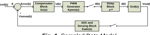
NTRODUCTIONThe aim of this paper is to describe the sampled data modeling of a switching regulator and the practical implementation of a digital compensator on an 8 bit microcontroller. The major blocks comprising a digital control loop are described and their transfer functions are derived. Practical issues involved in digital control using low cost 8 bit microcontrollers are discussed and results are presented. Modeling of switching regulators in continuous time domain is a well established discipline. Introduced by S. Cuk [1], the averaging approach for switching regulator modeling is a well known and widely popular technique. In this approach, the non-linear switching waveforms are averaged over one switching period thereby removing switching ripple and associated non-linearity. This is justified as in a well designed converter the switching ripple is small as compared to dc quantities. Small signal models can then be derived and used for control system design. The advantages of this approach are its simplicity and ease of use. Moreover, analog control design tools can be used for designing control systems. However, these models are accurate up to half of the switching frequency. Discreet time modeling of switching regulators was introduced by J. Packard [2]. In this approach, instead of averaging, converter waveforms are described at the instant of sampling [9]. This captures the behavior of converter at the sampling instant which is then extended over entire switching period. This modeling results in exact small signal models of switching regulators which can be used to design control systems using MATLAB. These models are accurate throughout the frequency range. However such models suffer from the complexity of the results as well as lack of close form results. Sampled data modeling approach introduced by A.R. Brown [3] combines the simplicity of average modeling approach with the accuracy of discreet time modeling technique. The entire system is modeled in continuous domain using conventional Laplace transform transfer functions. The delay associated with the digital control loops is modeling using a single delay block.
Gvd(s) Delay
Block e-st PWM
Generator Kpwm(s)
ADC and Sensing Block
Kadc(s) Compensator
Block Gc(s) Vref(k)
Vsense(k) Error(k) +
-U(k) d(k) d(t) Vout(t)
Fig. 1. Sampled Data Model
This retains the closed form results nature of the model and also incorporates the physical delays associated with the practical systems. In this work, a sampled data model of a buck converter is used to model the system and select compensator. The efficacy of the compensator designed is validated through MATLAB simulations. The digital loop is closed around an 8 bit microcontroller from ST Micro. The aim of this work is to provide an easy to understand derivation of sampled data model as well as demonstrate the capability of an 8 bit system to control a switching converter with acceptable performance for a given application. The paper is presented in following way: section 2 and 3 provide derivation of average circuit modeling approach and state space averaging approach for a special case of buck converter including inductor dc resistance and capacitor esr. It is assumed that the converter operates in continuous conduction mode. Section 4 provides description of transfer functions for various building blocks of a digital control loop. Section 5 provides simulation results of compensator designed in MATLAB as well as practical implementation details. Section 6 describes potential applications of this converter.
2. Average Circuit Modeling
We begin with the basic buck converter schematic as shown below. Note that inductor dc resistance and capacitor esr are ignored initially and will be incorporated later.
Vg(t)
L
C R
Diode MOSFET
Non-Linear Switching Portion
+
-V
(t)Fig. 2. Buck Converter _______________________
16 The aim of the modeling is to replace the non linear switching
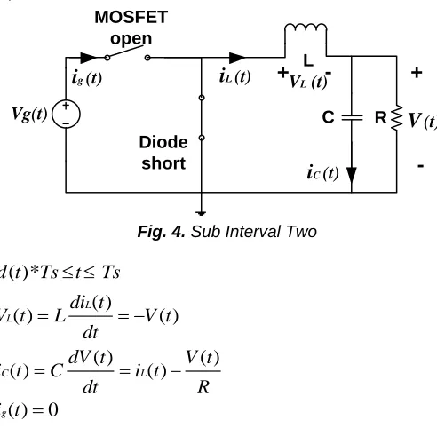
part of the converter with linear circuit elements so that the circuit can be solved for transfer functions using linear circuit analysis tools. The buck converter in continuous conduction mode operates periodically in two states; subinterval one in which MOSFET switch is ON and diode is off; subinterval two in which MOSFET switch is OFF and diode is ON. In first step, both these subintervals along with the equations describing inductor current and output voltage are shown:
Vg(t)
L
C R
Diode open MOSFET
short
i
L (t)V
(t)+
-+
V-L (t)
i
C (t)i
g (t)Fig. 3. Sub Interval One
0
t
d t
( )*
Ts
(1)( )
( )
L( )
( )
L g
di t
V t
L
V t
V t
dt
(2)( )
( )
( )
( )
C L
dV t
V t
i t
C
i t
dt
R
(3)
( )
( )
g L
i t
i t
(4)Where d(t) is the duty ratio function representing the time MOSFET switch is ON. Ts is the switching period. Equation (1) represent the time duration when MOSFET is ON.
Vg(t)
L
C R
Diode short MOSFET
open
i
L (t)V
(t)+
-+
V-L (t)
i
C (t)i
g (t)Fig. 4. Sub Interval Two
( )*
d t
Ts t
Ts
(5)( )
( )
L( )
L
di t
V t
L
V t
dt
(6)( )
( )
( )
( )
C L
dV t
V t
i t
C
i t
dt
R
(7)
( )
0
g
i t
(8)
Applying the averaging operator <x(t)>Ts [4] to these equations
and combining for both intervals using duty cycle functions d(t) and d’(t),where d(t) represents the time of switching period during which MOSFET is ON and d’(t) = 1-d(t), we arrive at large signal model of buck converter:
( )
[
( )
( )
]* ( )
[
( )
]* '( )
L Ts
Ts Ts
Ts
d
i t
L
Vg t
V t
d t
dt
V t
d t
(9)
( )
( )
( )
Ts Ts
L Ts
d
V t
V t
C
i t
dt
R
(10)
( )
( )
* ( )
g Ts L Ts
i t
i t
d t
(11)The above equations describe the large signal model of the buck converter. In order to derive the small signal model of the buck converter, a steady state solution is assumed to exist (Vg, V, I, D) and following variables are perturbed and linearized:
( )
( ),
( )
( ),
( )
( ),
( )
( ),
( )
( ),
'( )
( )
g Ts g g g Ts g g
Ts L Ts L
V t
V
v t
i t
I
i t
V t
V
v t
i t
I
i t
d t
D
d t
d t
D
d t
(12)
Where the small perturbation in x(t) is denoted as x̂(t) and it is further assumed in accordance with small ripple approximation that: x̂(t) << X i.e. the perturbation is very small as compared to dc quantities. Equations (9), (10) and (11) become:
[
( )]
[
( )
( )]*[
( )]
[
( )]*[
( )]
L
g g
d I
i t
L
V
v t
V
v t
D
d t
dt
V
v t
D
d t
(13)
[
( )]
( )
( )
L
d V
t
V
v t
C
i t
dt
v
I
R
(14)[
( )]*
( )
[
( )]
g g
i t
LI
i t
I
D d t
(15)After ignoring DC and higher order terms, one arrives at the small signal model of buck converter:
( )
[ * ( )] [
* ( )]
( )
L
g g
di t
L
dt
D v t
V
d t
v t
(16)( )
( )
( )
Ld v t
C
dt
v t
i t
R
(17)[
*
( )
( )] [ ( )* ]
g
D
Li t
i t
d t
I
(18)And the equivalent circuit is shown below:
vg(t)
L
C R
+
-v (t)
d (t)*I ig (t)
1 : D
Vg*d(t) iL (t)
Linear Circuit Elements
Fig. 5. Equivalent Average Circuit Model
17 side voltage source vĝ (t) is set to zero so as to assume zero
variation in supply voltage. This result in elimination of dc transformer and following circuit is obtained.
sL
1/sC R
+
-v
(s)Vg* (s)
i
L (s)rl
rc
Z2(s) Z1(s)
Fig. 6. Equivalent Impedances
Here rl and rc represent the dc resistance of inductor and esr of capacitor respectively. Also all the impedances are represented in Laplace domain. This circuit can be very easily simplified to obtain Gvd(s) using voltage divider rule as shown below:
( ) * 2( ) ( )
1( ) 2( ) ( )
g vd
v s V Z s
G s
Z s Z s
d s
(19)
1
1( )
,
2( )
|| (
)
Z s
rl
sL
Z
s
R
rc
sC
(20)2
* * ( * * 1) ( )
* * * ( ) * ( * * * * ( )
vd
g G
V R s C rc
s
s L C R rc s L rc rl C R C rc rl R rl
(21)
This is the desired control to output transfer function and coincides with the results such as those given in [7].
3. State Space Average Modeling
The general state space representation of a switching converter is given by following two equations [4]:
( )
( )
* ( )
* ( )
d x t
d t
A x t
B u t
(22)
( )
* ( )
* ( )
y t
C x t
E u t
(23)Where x(t) is the state vector of the system consisting of inductor current and capacitor voltage and is given by:
( )
( )
( )
LC
i t
x t
V t
(24)U(t) is the system input vector which consists of input source
Vg(t). We define the state vectors in the following manner [4]:
* 1
' * 2
* 1
' * 2
* 1
' * 2
* 1
' * 2
A
D A
D
A
B
D B
D
B
C
D C
D
C
E
D E
D
E
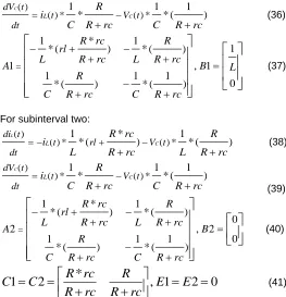
(25)Where D and D’ are duty ratio and its complement respectively. In order to derive state space average model including the effects of inductor dc resistance and capacitor esr, following circuits are used for subinterval one and subinterval two respectively:
Vg(t)
L
C R
Diode open MOSFET
short
iL (t)
v(t)
+
-+
-vL (t)
iC (t)
ig (t) rl rc
+
-Vc(t)
Fig. 7. Sub Interval one
0
t
d t
( )*
Ts
(26)( )
( )
L( )
( ) *
( )
L
di t
g LV t
L
V t
i t
rl V t
dt
(27)( )
( )
( )
( )
C L
C
dV t
V t
i t
C
i t
dt
R
(28)Vg(t)
L
C R
Diode short MOSFET
open
iL (t)
v(t)
+
-+
-vL (t)
iC (t)
ig (t) rl rc
+
-Vc(t)
Fig. 8. Sub Interval Two
( )*
d t
Ts t
Ts
(29)( )
( )
L( ) *
( )
L
di t
LV t
L
i t
rl V t
dt
(30)( )
( )
( )
( )
C L
C
dV t
V t
i t
C
i t
dt
R
(31)
The output voltage V(t) is due to two state variables iL(t) and
VC(t). We use superposition to obtain V(t). V(t) due to iL(t):
short circuit VC(t), we use current divider rule:
( )
rc
* ( ) *
LV t
R
rc
i t
R
(32)V(t) due to VC(t): open circuit iL(t), we use voltage divider rule:
( )
R
*
C( )
V t
R
rc
V t
(33)( )
*
C( )
* ( ) *
LR
rc
V t
R
rc
V t
R
rc
i t
R
(34)The result coincides with the one in [8]. Replacing the value of V(t) in above equations:
( )
( ) ( ) * ( ) *
1 1 * 1
* * ( ) * ( )
L
g L C
di t
V t t rl V t
dt
R rc R
i
L L R rc L R rc
18
( )
( ) *1* ( ) *1* ( 1 )
C
C
L
dV t
t V t
dt
R i
C R rc C R rc
(36)
1 * 1
1
* ( ) * ( )
1 , 1
1 1 1
0
* ( ) * ( )
R rc R
rl
L R rc L R rc
A B L
R
C R rc C R rc
(37)For subinterval two:
( )
( ) *1* ( * ) ( ) *1* ( )
L
C
L
di t
t rl V t
dt
R rc R
i
L R rc L R rc
(38)
( )
( ) *1* ( ) *1* ( 1 )
C
C
L
dV t
t V t
dt
R i
C R rc C R rc
(39)
1 * 1
* ( ) * ( )
0
2 , 2
1 1 1 0
* ( ) * ( )
R rc R
rl
L R rc L R rc
A B
R
C R rc C R rc
(40)*
1
2
R rc
R
, 1
2
0
C
C
E
E
R
rc
R
rc
(41)After state matrices have been calculated, the small signal control to output transfer function can be easily calculated using the following equations [4]:
( )
( )
* ( ) * ( ) [(A1 A 2) * X (B1 B 2) * U] * d(t)
d t
d t
x
A x t B u t
(42)
* ( ) * ( ) [( 1 2) * X ( 1 2) * U] * d(t)
( )
C x t E u t C C E Ey t
(43)where X and U are the dc state and input matrices given as:
X = [IL Vc] T
and U =[Vg] (44)
We assume zero input supply disturbances and take Laplace transform of the remaining equations with following parameters:
1 2, 1, 2 0, 1 2, 1 2 0
AA A BB B CC C EE E (45)
* ( ) * ( ) B* U* ( )
s x s A x s d s (46)
( ) * ( * ) B* U* ( )
x s s IA d s (47)
1
( ) ( * ) * B* U* ( )
x s s IA d s (48)
Also:
( )s
* ( )
y
C x s
(49)1 ( )
*( *
) * *
( )
sy
C
s I
A
B U
d s
(50)The above equation can be easily solved using MATLAB to obtain desired control to output transfer function.
4. Digital Control Loop
The general digital control loop implemented around a microcontroller is shown below:
Gvd(s) Delay Block e-st PWM Generator Kpwm(s) ADC and Sensing Block Kadc(s) Compensator Block Gc(s) Vref(k) Vsense(k) Error(k) +
-U(k) d(k) d(t) Vout(t)
Fig. 9. Digital Control Loop
The output voltage is sampled by ADC at sampling frequency equal to switching frequency. The discreet error is processed by compensator and built in PWM module generates pulses with duty cycle as provided by compensator block. The modulation and processing delays are lumped in a single delay block as shown. There are various blocks in the system which are described as under:
4.1 Power Stage
The power stage of a switching regulator is modeled using either average circuit modeling approach or state space averaging approach as described in section 2 and 3 respectively. The modeling of the power stage is necessary to completely understand the dynamics of power stage and to explicitly model the effects of parasitic elements such as inductor and capacitor dc resistances. The converter transfer function Gvd(s) is usually control to output voltage transfer function, however other parameters such as inductor current can also be used as controlled variable.
4.2 ADC and Sensing Block
19 Vout
R1
R2
Kdiv = R2/ (R1+R2)
+
-Voltage Follower Rf
Cf
Kfilter = 1/(1+s/wf) wf=1/Rf*Cf Vsense
8-Bit ADC
Kquantization = 256
Fig. 10. ADC and Sensing Block
The complete gain of the sensing stage is:
( )
*
( )*
Kadc s
Kdiv Kfilter s
Kquantization
(51)4.3 PID Compensator
The design of compensators for switching regulators is a well established discipline in analog domain. The transfer function of power stage is used to determine the type of compensation required, namely type 2 or type 3. PID compensators (two zeros and one integrator) have also been used to control switching regulators [5]. The advantage of PID controller, apart from its easy implementation, is the high phase boost provided by the pair of zeros as well as steady state regulation provided by single pole at origin. For these reasons, a PID regulator is a suitable choice for implementation on 8 bit microcontrollers [6]. The general transfer function of PID regulator in continuous domain is given as:
( )
Ki
*
Gpid s
Kp
Kd s
s
(52)Using Euler’s method, the transfer function is converted to a discreet difference equation for implementation in controller as follows:
( ) * ( ) * * ( ) *[ ( ) ( 1)]
d k Kp e k Ki Ts e k Kd e k e k
Ts
(53)Where e(k) is the discreet error and d(k) is the discreet duty cycle output from the PID controller. The gains of the PID compensator are selected as powers of two. This makes the implementation of PID compensator with the limited resources of an 8 bit microcontroller possible. The time taken to determine the duty cycle from equation above is critical as it directly affects the loop delay. To minimize duty cycle calculation time, shift operations are used instead of multiplication operation.
4.4 PWM Modulator
The output of the compensator block is passed to PWM generator. In microcontroller systems, the PWM generator is counter based PWM block. This puts limits on the maximum frequency and output voltage sensing resolutions. For example, if 16 MHZ clock is used to generate 100 KHZ PWM, then timer period value is 16M/100K = 160. Now, with input voltage of 20V, one bit change in duty cycle value will correspond to 20 V/160 = 125mV change in output voltage. Therefore the minimum value of output voltage change that can induce one bit change in ADC value must be greater than 125mV in order to avoid limit cycle oscillations. The value of the compensator output is so limited that the minimum and maximum values correspond to the minimum and maximum
duty cycles respectively.
1
( )
Kpwm s
Timer Period Value
(54)The timer period value is dependent upon the microcontroller clock frequency for a given system.
4.5 Delay Block
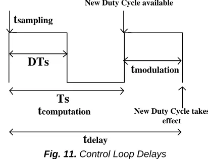
In digital control loops, two types of delays are present [10]. First delay is due to ADC conversion and compensator block calculations. This delay is called computational delay. Second delay is due to the fact that any change in the value of duty cycle becomes visible only after the falling edge has occurred. This is called modulation delay. This is illustrated in following figure.
DTs
t
samplingNew Duty Cycle available
New Duty Cycle takes effect
Ts
t
computationt
modulationt
delayFig. 11. Control Loop Delays
The above figure shows the case when entire switching cycle is required for duty cycle calculation as is the case of 8 bit systems. As can be seen, duty cycle change takes effect only after falling edge of PWM train and hence the resulting modulation delay. In 8 bit systems, the system computational power limits the time available for control law calculation as well as ADC conversion. Therefore, a complete switching cycle is dedicated to ADC conversion and duty cycle calculation. For a steady state duty cycle of 0.5, the total delay is 1.5 Ts, where Ts is the switching period. Duty cycle calculated in current switching interval is used in the next switching interval and so on.
( )
tdGdelay s
e
(55)4.5 Loop Gain
The complete loop gain of the system is the product of the individual gains of all the blocks that comprise the system and is given as:
( ) ( ) * ( ) * ( ) * ( ) * ( )
T s Gvd s Kadc s Gpid s Kpwm s Gdelay s (56)
5. Buck Converter Example
20 the author, available in any 8 bit microcontroller system. The
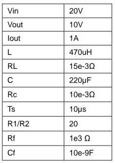
ADC has a fixed 10 bit resolution. This can be a detrimental keeping in view the fact that PWM resolution at 100 KHz switching frequency is lower than 10 bits. However, using external voltage divider and by compromising on output voltage resolution (contingent upon application), one can avoid limit cycle oscillations. The following table shows the buck converter parameters used to demonstrate the example:
Table 1 Buck Converter Parameters
Vin 20V
Vout 10V
Iout 1A
L 470uH
RL 15e-3Ω
C 220µF
Rc 10e-3Ω
Ts 10µs
R1/R2 20
Rf 1e3 Ω
Cf 10e-9F
The schematic diagram of the system is shown next:
20 V
470µH
10Ω 1N4007
IRF3205
+
-v(t)
15mΩ 10mΩ
220µF
Gate Driver Circuit IR2110
Timer based PWM Block
ADC
PID Compensator
Block
R1
R2
Kdiv = R2/(R1+R2)
+
-Voltage Follower Rf
Cf
STM8S105C8T6
Fig. 12. Schematic of Buck Converter Controlled by STM8S
5.1 MATLAB Simulation
The transfer functions of the various blocks are provided next:
7 2
( )
0.0004*
200
9.409
*
0.00052*
10.02
Gvd s
s
e
s
s
(57) 65
( )
5.1
1
Kadc s
e
s
e
(58) ( )0.00063
Kpwm s (59)
1.5*
( ) Ts
Gdelay s
e
(60)The uncompensated Loop gain is obtained by setting compensator transfer function to unity:
1.5*
( ) ( ) * ( ) * ( ) * Ts
Tu s Gvd s Kadc s Kpwm s e (61)
6
7 3 2 6
1.5 5* ( )
12.75 * 6.375
9.409 * 0.0946 * 62.02 * 1
e s
Tu s e
s e
e s s s e
(62)
The bode plot of the uncompensated loop gain is obtained in MATLAB.
Fig. 13. Bode Plot - Uncompensated System
The phase margin comes out to be -7.48ᵒ. It should be emphasized here that by using an 8 bit microcontroller, the main parameter of interest is the phase margin of the system. The bandwidth of the system is of secondary importance as the proposed applications of this particular converter do not require very fast speed of the control loop. We select the zeros of PID controller as shown below:
2
( )
0.125*
64*
16
512*
Gpid s
s
s
s
(63)The resulting bode plot of the compensated system is shown below:
Fig. 14. Bode Plot - Compensated System
The gain margin comes out to be 68ᵒ with a cutoff frequency of 2.7 KHz. It should be noted that the zeros of PID controller are selected such that after simplification, the individual gains Kp,Ki and Kd come out to be powers of 2 which helps in implementation.
5.2 Practical Implementation
21 available. Although assembly language implementation
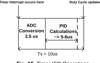
provides much faster code, implementation in C language is far easy and practical and is used for this application. A timer available in the STM8S controller is used to generate duty cycle controlled PWM waveform as well as implement compensation algorithm. The timer is configured for PWM of 100 KHz with interrupt on the timer overflow event, which is the event at which the timer starts recounting. In interrupt service routine, ADC conversion of output voltage and compensation algorithm are implemented sequentially. The duty cycle can only be updated at the beginning of the timer cycle. Therefore, a complete switching cycle is dedicated for ADC conversion and control law implementation. This is the worst case scenario and is inevitable in an 8 bit controller with very limited computational power. However with proper implementation, it can still provide acceptable performance.
ADC Conversion
2.5 us
PID Calculations
~= 5-6us
Ts = 10us
Timer Interrupt occurs here Duty Cycle updated
Fig. 15. Timer ISR Operations
The flowchart of the main ISR used to implement the controller is shown below:
Timer ISR
Clear Interrupt Flag
Start ADC Conversion
Vout = Read ADC Data
Error = Vref - Vout
Kp = error * Kp_gain
Limit Kp
Integral_Sum += error * Ki_gain1
Limit Integral_Sum
Kd = (error – error_1) * Kd_gain
Limit Kd
Duty_cycle = Kp + Ki + Kd
Limit Duty_cycle
Load Duty_cycle Ki = sum *Ki_gain2
Fig. 16. Timer ISR
All the variables used in the software are signed or unsigned integers. The programmer should take care of implicit conversion between signed and unsigned conversions as this can lead to hard to track errors. In 8 bit systems, the computational power as well as time available for control loop is limited, therefore simple integers are used instead of number representations which are more suitable for high
speed DSPs. Also it should be noted that the controller outputs Kp, Ki and Kd are limited in addition to duty cycle limits. Such limits do effect the controller behavior but are necessary for practical reasons such as noise and register over runs. Such limits should be decided dynamically after practical measurements and observations. Apart from this, it should be noted that gain such as Ki is implemented in stages. This is done because it results in more stable operation as observed practically. The practical setup on bread board along with STM8S discovery kit is shown next:
Fig. 17. Practical Setup
Fig. 18. Steady State Output Voltage
As can be observed, the output voltage is steady at a constant level without limit cycle oscillations.
Fig. 19. Startup Response
22 on the actual gains in controller implementation which are
necessary due to practical reasons.
6. POTENTIAL APPLICATIONS
This paper presented a digitally controlled buck converter using an 8 bit microcontroller. One might wonder the scope of applications where this controller might be used. Although analog and DSP based digital controllers provide far better dynamic and steady state performances and have been well established, yet not every application warrants use of such costly (DSP based) or inflexible (analog) solutions. Ease of implementation, flexibility and low cost are the key merits of this 8 bit microcontroller based converter. Potential applications can be battery charging, maximum power point tracking, dc-dc converters in ups applications (12V to 400 V converters). Although an 8 bit controller with 16 MHZ clock was used for this application, the system clock in 8 bit systems can be increased upto 48 MHZ which can provide further performance boost and flexibility in human machine interface implementation. Moreover, in this application, 100KHZ was the switching frequency selected for buck converter which is a reasonable frequency for most dc-dc converter applications.
7. CONCLUSION
This paper presented mathematical modeling of a buck converter including the effects of parasitic such as inductor dc resistance and capacitor esr. A sampled data model of digitally controlled buck converter system was derived next. A suitable PID controller was selected to obtain the satisfactory control loop performance. MATLAB simulation and practical implementation results were presented to validate the theoretical work. It is believed that such low cost controller can be successfully employed in battery charging and similar applications.
REFERENCES
[1] Middlebrook, R.D., Cuk, S., “A general unified approach to modeling switching power converter stages,” Proceedings of Power Electronics Specialists Conference, 1977
[2] Packard, D. J., “Discrete Modeling and Analysis of Switching Regulators”, Ph.D Thesis, California Institute of Technology, Pasadena California, 1976.
[3] Brown, A. R., “Topics in the Analysis, Measurement and Design of High-Performance Switching Regulators”, Ph.D Thesis, California Institute of Technology, Pasadena California, 1981.
[4] Erickson, R.W., Maksimovic, D., “Fundamentals of Power Electronics”, 2nd
Edition, Kluwer Academic Publishers, 2000.
[5] Erickson, R.W., et.al, “Design and Implementation of a Digital PWM Controller for a High-Frequency Switching DC-DC Power Converter,” IECON’01: The 27th
Annual Conference of the IEEE Industrial Electronics Society.
[6] Nelms, R.M., et.al, “Simulation and Modeling of a DC-DC Converter Controlled by an 8-bit Microcontroller,” Department of Electrical Engineering, Auburn University.
[7] Miftakhutdinov, R., “Compensating DC/DC Converters with Ceramic output capacitors”, Texas Instruments Applications Note.
[8] Tzou, Y.Y., Jung, S.L., “Full Control of a PWM DC-AC Converter for AC Voltage Regulation”, IEEE Transc. On Aerospace and Electronic Systems, Vol. 34, No. 4,October 1998.
[9] Maksimovic, D., et al. “Digital Control of High Frequency Switched Mode Power Converters”, 1st