A Study on the Impact of Nothing (SON) Versus
Silicon-on-Insulator (SOI) on the Electrostatic Performance of a Transistor
Noraini Othman1*, S. N. Sabki1 and H. Aris1
School of Microelectronic Engineering, Universiti Malaysia Perlis, Pauh Putra Campus, 02600 Arau, Perlis, Malaysia.
ABSTRACT
In this work, we investigate the impact of employing silicon-on-nothing (SON) versus silicon-on-insulator (SOI) on the electrostatic performance of a transistor with various ground-plane (GP) structures of Lg = 10 nm through the use of Sentaurus TCAD simulator. The digital figure-of-merit (FoM) of interest includes the results of drain-induced barrier lowering (DIBL) which is a major indicator of a control of short-channel effects (SCEs). It is found that SOI devices produce a lower off-current (Ioff) as compared to SON. In terms of the different GP architectures, the introductions of various GP architectures were found to affect the values of DIBL in SOI whereas the impact on SON is negligible. It can be concluded that GP-B architectures with ground plane underneath the channel areas of SOI is most effective in suppressing substrate depletion effects as evidenced from the lowest DIBL produces.
Keywords: Silicon-on-Nothing; Silicon-on-Insulator, DIBL, SCEs, Ground-Plane, CMOS.
1. INTRODUCTION
The continuous down scaling of the conventional complementary metal-oxide-semiconductor field-effect transistor (CMOS) is the major booster for the growth of the semiconductor industry. However, as the scaling of conventional CMOS is approaching technological limits, there is a growing need for replacement technology and device architecture. An interesting alternative approach is given by silicon-on-nothing (SON) and silicon-on-insulator (SOI). SON is an efficient solution for parasitic substrate coupling suppression through the substrate on the transistor behavior. The ‘nothing’ region is obtained by the selective removal of silicon-dioxide layer [1]. Meanwhile, in a SOI technology, a layer of buried silicon dioxide (BOX) is used to isolate a thin layer of silicon from the silicon substrate. Short-channel effects (SCEs) in SOI devices are related to the doping density of thin-film, the thickness of thin-film, the substrate biasing, the thickness of buried oxide and the processing technology. When a very thin BOX is being used, the coupling between the gate and substrate is stronger which may cause both the static behaviour and the frequency response of the device to deteriorate depending on the space-charge conditions at the substrate-BOX interface. If the substrate is lightly-doped, the space-charge will be depleted by the gate and drain electric fields and behave as a dielectric. This will cause the depleted layer to be effectively added to the physical oxide thickness of the BOX [2], and the thin BOX loses its advantages. Thus, ground plane (GP) architectures are used to suppress the fringing electric fields through the substrate [3]–[6]. In this work, we perform an analytical comparison to understand the relative performance of SON and SOI MOSFET, together with implementations of various GP architectures to uncover their impacts towards the electrostatic performance of the device.
154
2. METHODOLOGY
2.1Simulation Methodology
Figure 1. Device structure for std-GP, GP-A and GP-B on (a) SOI and (b) SON.
The simulations were performed using Sentaurus TCAD Tools in 2D. Various ground plane (GP) architectures for both SON and SOI devices as in Figure 1 were simulated to determine the effectiveness of the structure in supressing substrate depletion effects. The transistor simulated is of gate length, Lg = 10 nm, buried oxide thickness, TBOX = 10 nm and silicon-body thickness, Tsi
= 7 nm. The channel is undoped with 6.5x1014 cm-3 of acceptor concentrations [7] while S/D are
doped with 1x1020 cm-3 of donor concentrations. An effective oxide thickness (EOT) of 1.2 nm
and metal gate work function, of 4.65 eV are used. Apart from the difference in SON and SOI structure, comparisons are also being made between the different GP architectures , i.e. standard ground plane (std-GP), ground plane A (GP–A) and ground plane B (GP–B). The std-GP consists of P+ dopant concentration of 1x1018 cm-3 of thin layer underneath the BOX area. For
GP-A, P+ dopant concentration of 1x1020 cm3 is made under the S/D area [8]. In GP-B, P+
concentration of 1x1018 cm3 is formed under the channel. It has been demonstrated in [9][10]
that these architectures can be built in a self-aligned manner with a localized highly doped regions formed in the substrate underneath the BOX.
The physical model used in the simulation includes the Shockley-Read-Hall (SRH) recombination model where the carrier lifetimes depend on the doping level, temperature and electric field. Meanwhile, Lombardi mobility model was used in order to include the parallel and perpendicular electric fields. The band gap narrowing (caused by heavy doping) as a result of shrinkage of bandgap when impurity concentration increases was also considered for the carrier statistics. Hydrodynamic model that takes into account the transfer of energy and lattice heatings was also included. The device is operated at a power supply voltage of 1.5 V. For the analysis of the digital figure of merit (FoM), graphs of drain current versus gate voltage (Id–Vg)
are plotted at Vd = 20 mV and 1.0 V, while Vg is swept from 0 V to 1.5 V.
155
3. RESULTS AND DISCUSSIONS
3.1 Drain Current-Gate Voltage (Id –Vg) Characteristics
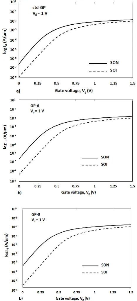
Figure 2. Id-Vg characteristics showing SON vs SOI for (a) std-GP (b) GP-A and (c) GP-B structures at Vd = 1
156
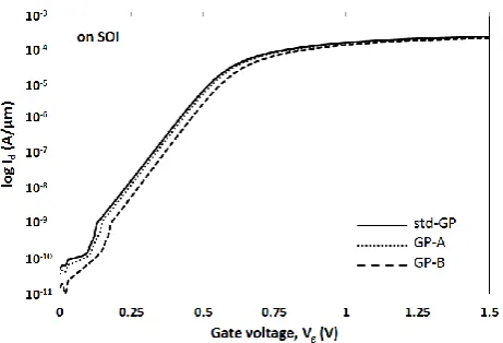
Figure 3. logid-vg for soi with various gp architectures at vd = 20 mv.
Figure 2 (a) – (c) show the Id - Vg characteristics for a std-GP, GP-A and GP-B architectures for
SON and SOI respectively. It is found that for all three GP architectures, SON exhibits a slightly higher on-current, Ion as compared to SOI. However, this advantage was overridden as the
off-current, Ioff of SON was significantly higher by about 1- 2 magnitude throughout std-GP, GP-A
and GP-B architectures. Meanwhile, in terms of the different GP architectures, it is found that different GP architectures affect the corresponding Ion and Ioff for SOI as shown in Figure 3.
However, it is found that different GP architectures does not give any impact on SON, thus the results are not shown.
3.2 Drain-Induced Barrier Lowering (DIBL)
Table 1 DIBL for various GP architectures with SON and SOI of Lg = 10 nm
GP Structures DIBL (mV/V) with SON DIBL (mV/V) with SOI
Std-GP 224 224
GP-A 224 199
GP-B 224 179
DIBL refers to reduction in barrier height for channel carriers at the edge of the source as a result of drain electric field upon application of high drain voltage, and is an important indicator of SCEs [11]. DIBL in this work is defined as the difference in threshold voltage, Vth when the
drain voltage, Vd is increased from 0.02 V (linear mode) to 1 V (saturation mode). In other
words, DIBL = [(Vthlin – Vthsat) / (Vdsat – Vdlin)], where Vth extraction in this work is performed
using a constant-current method where Vth is taken as the intercept of Vg axis of the Id-Vg
characteristic at drain current, Id = 1x10⁻⁷ A/µm. Table 1 shows the results of DIBL for different
GP architectures for SON and SOI respectively. It can be seen that by employing SON, implementation of different GP architectures did not give any effects. However, it is found that different GP architectures in SOI give a significant impact towards the corresponding DIBL results, with GP-B architecture producing the lowest DIBL. Thus, it can be concluded that GP-B architecture with the implementations of p-type doping underneath the channel areas effectively suppress the substrate depletion effects.
4. CONCLUSIONS
In this work, we investigate the effectiveness of implementing different GP architectures in suppressing substrate depletion effects for SON and SOI devices. It is found that although the implementation of GP architectures managed to produce a slightly higher Ion in SON devices, this
advantage was counteracted by the significantly higher Ioff. Further investigation shows that
157
devices. In SOI devices, GP-B architecture was found to produce the lowest DIBL among all other architectures which is translated into its effectiveness in curbing substrate depletion effects and ultimately the SCEs.
REFERENCES
[1] T. M. Chung, B. Olbrechts, U. Södervall, S. Bengtsson, D. Flandre & J. P. Raskin, “Planar double-gate SOI MOS devices: Fabrication by wafer bonding over pre-patterned cavities and electrical characterization,” Solid. State. Electron. 51, 2 (2007) 231–238.
[2] C. Fenouillet-Beranger, T. Skotnicki, S. Monfray, N. Carriere & F. Boeuf, “Requirements for ultra-thin-film devices and new materials for the CMOS roadmap,” Solid. State. Electron.,
48, 6 (2004) 961–967.
[3] C. Fenouillet-Beranger, S. Denorme, P. Perreau, C. Buj, O. Faynot, F. Andrieu, L. Tosti, S. Barnola, T. Salvetat, X. Garros, M. Cassé, F. Allain, N. Loubet, L. Pham-Nguyen, E. Deloffre, M. Gros-Jean, R. Beneyton, C. Laviron, M. Marin, C. Leyris, S. Haendler, F. Leverd, P. Gouraud, P. Scheiblin, L. Clement, R. Pantel, S. Deleonibus & T. Skotnicki, “FDSOI devices with thin BOX and ground plane integration for 32nm node and below,” Solid. State. Electron. 53, 7 (2009) 730–734.
[4] R. Yan, R. Duane, P. Razavi, A. Afzalian, I. Ferain, C. Lee, N. D. Akhavan & B. Nguyen, “LDD and Back-Gate Engineering for Fully Depleted Planar SOI Transistors with Thin Buried Oxide,” IEEE Trans. Electron Devices 7, 6 (2010) 1319–1326.
[5] M. Saremi, B. Ebrahimi, A. A. Kusha, M. Saremi & K. Abad, “Process Variation Study of Ground Plane SOI MOSFET,” in 2nd Asia Symposium on Quality Electronic Design 6, (2010) 66–69.
[6] C. Fenouillet-Beranger, P. Perreau, S. Denorme, L. Tosti, F. Andrieu, O. Weber & S. Monfray, “Impact of a 10 nm ultra-thin BOX ( UTBOX ) and ground plane on FDSOI devices for 32 nm node and below,” Solid State Electron. 54, 9 (2010) 849–854.
[7] V. Kilchytska, D. Levacq, D. Lederer, G. Pailloncy, J. Raskin & D. Flandre, “Substrate Effect on the Output Conductance Frequency Response of SOI MSOFETs,” in Nanoscaled Semiconductor-on-Insulator Structures and Devices, S. Hall, A. . Nazarov, and V. S. Lysenko, Eds. Dordrecht: Springer, (2007) 221–238.
[8] H. Makiyama, Y. Yamamoto, T. Tsunomura, T. Iwamatsu, K. Sonoda, H. Oda, N. Sugii & Y. Yamaguchi, “Novel Local Ground-Plane Silicon on Thin BOX ( SOTB ) for Improving Short-Channel-Effect Immunity,” in Euro SOI 2, January (2012) 27–28.
[9] W. Xiong & J. P. Colinge, “Self-aligned implanted ground-plane fully depleted SOI MOSFET,” Electron. Lett. 35, 23 (1999) 2059–2060.
[10] W. Xiong, K. Ramkumar, S. J. Jang, J.-T. Park & J.-P. Colinge, “Self-Aligned Ground-Plane FDSOI MOSFET,” in IEEE International SOI Conference, (2002) 23–24.