E-mail: {m5201118, m5191117, hiroshis}@u-aizu.ac.jp
Keywords:asynchronous circuits, FPGAs, processors
Received:November 18, 2016
In this paper, we propose a modeling method and a design flow to design asynchronous processors with bundled-data implementation on commercial Field Programmable Gate Arrays (FPGAs). The modeling method mainly concerns modeling of an asynchronous control circuit on commercial FPGAs. In addition to the use of a design environment provided by FPGA vendor, the design flow includes constraint generation, timing analysis, and delay adjustment to design asynchronous processor from a prepared model to FPGA programming. In the experiments, we design three asynchronous MIPS processors. Comparing with the synchronous counterpart, one of them reduces global cycle time which results in 13.8% performance improvement and another one reduces energy consumption 9.3% for a multiplication and 8.8% for a matrix multiplication.
Povzetek: Opisan je razvoj novega sinhronega procesorja na osnovi tržnega FPGA.
1
Introduction
Field Programmable Gate Arrays (FPGAs) are reconfig-urable circuits where circuit structure can be changed by designers freely. Therefore, compared to Application Spe-cific Integrated Circuits (ASICs), the lifetime of FPGAs is long. In addition, the design cost is low because FPGA vendors provide the design environment free of charge. Re-cently, due to the advance of the FPGA technology, FPGAs are well adopted in embedded systems and servers for data centers [1]. As there are a rich number of resources on FPGAs, we can accelerate performance by implementing Multi-Processor System-on-Chip (MPSoC). Current ad-vanced FPGAs such as Altera Cyclone V include an ARM Cortex processor as a hard-macro to support MPSoC.
Most of commercial FPGAs are synchronous circuits. Circuit components in synchronous circuits are controlled by global clock signals. In synchronous circuits, clock skew, power consumption, and electromagnetic radiation will be significant problems when the semiconductor sub-micron technology is advanced more and more. In addi-tion, generally, the power efficiency of FPGAs is worse than ASICs. Therefore, low power designs on FPGAs are very important.
Compared to synchronous circuits, circuit components in asynchronous circuits are controlled by local hand-shake signals. Due to the absence of global clock sig-nals, asynchronous circuits are potentially low power con-sumption and low electromagnetic radiation. Therefore, asynchronous circuits may be useful for FPGAs where low power design is important. However, the design of achronous circuits is more difficult than the design of
syn-chronous circuits. To represent circuit behaviors, circuit model including delay model, data encoding scheme, and handshake protocol should be considered. Based on the considered model, asynchronous circuits are designed. In addition, asynchronous circuit designs are also difficult for commercial FPGAs because the design environment pro-vided by FPGA vendors is assuming synchronous circuit designs.
Figure 1: Circuit structure of asynchronous circuits with bundled-data implementation.
In this paper, we propose a modeling method and a de-sign flow to dede-sign asynchronous processors with bundled-data implementation on FPGAs. We address how to im-plement an asynchronous control circuit on the commer-cial FPGAs, how to synthesize the asynchronous processor with the generation of design constraints, and how to carry out timing verification correctly. We design three pipelined MIPS processors using the proposed method and design flow to evaluate area, execution time, dynamic power, and energy consumption.
The rest of this paper is organized as follows. In section 2, we describe asynchronous circuits with bundled-data im-plementation. In section 3, we describe about FPGAs. In section 4, we describe the proposed modeling method and design flow. In section 5, we describe the experimental re-sults by designing three MIPS processors. Finally, in sec-tion 6, we conclude this work.
2
Asynchronous circuits with
bundled-data implementation
Asynchronous circuits with bundled-data implementation shown in Fig.1 are one of data encoding schemes in asyn-chronous circuits. Timing of data operations is guaranteed by delay elements on request signals. Therefore, the per-formance depends on the delay of the control circuit. Com-pared to other implementations such as dual-rail implemen-tations [7] where one bit signal is represented by two wires and the completion detector is required, bundled-data im-plementation can be realized easily because we can use the same data-path resources as synchronous circuits. In addi-tion, the circuit area and the power consumption become smaller and lower than other implementations.
2.1
Circuit model
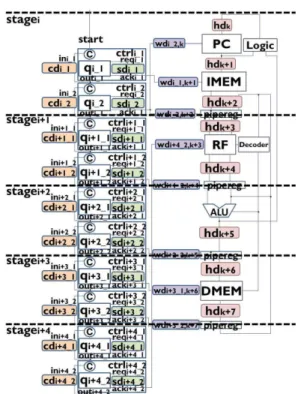
Figure 2 represents a bundled-data implementation model used in this paper. It is a pipelined processor model with several pipeline stagesi. The left side is the control circuit and the right side is the data-path circuit. The data-path cir-cuit consists of Program Counter (PC), Memories (IMEM and DMEM), pipeline registers (pipereg), Decoder, Reg-ister File (RF), ALU, and delay elementswdi,k andhdk.
PC stores the address of the instruction memory. IMEM
Figure 2: An asynchronous processor model with bundled-data implementation.
is a memory to store instructions. DMEM is a memory to store data. piperegs are registers to separate pipeline stages. RF is a collection of registers. Data from DMEM and ALU are written into RF.wdi,kandhdk are delay
ele-ments for registers or memories to guarantee simultaneous writing constraints and hold constraints.
The control circuit consists of control modules ctrli_j
(j= 1,2). A control modulectrli_jconsists of a Q-module
qi_j [8], delay elementssdi_j andcdi_j, and a C-element
ci_j [7].sdi_jis used to guarantee setup constraints. cdi_j
is used to guarantee control initialization constraints. The C-elementci_jis a synchronization component. The output
of the C-element is 0 when all inputs are 0. The output is 1 when all inputs are 1. Otherwise, the output does not change. Logical 1 for the output of the C-element means that the execution at the previous control module and the initialization of the current control module finish.
There are two notes in the control circuit. First, com-pared to ordinal asynchronous pipelined circuits such as Micropipelines [9] where a feedback signal for the C-element is generated from the output of the C-C-element in the next control module, the feedback signal in this control circuit is generated fromouti_j. This is because to keep the
same execution time in all pipeline stages. Second, we use two control modulesctrli_1andctrli_2to control a pipeline stageito hide the overhead caused by handshake signals.
Control modulesctrli_j operate as follows. When the
execution at the previous control module and the initializa-tion of the current control module finish,ci_jassertsini_j
Figure 3: Data-pathsdpi,land control pathscpi,lfor setup
constraints: (a) forward path and (b) backward path.
reqi_j. After the signal passes tosdi_j, it is returned toqi_j
with the assertion ofacki_j. Then, the Q-moduleqi_j
de-assertsreqi_j. After the signal passes tosdi_j again, it is
returned toqi_jwith the deassertion ofacki_j. The
deasser-tion ofacki_jassertsouti_jto move the control to the next
control module. Memories and registers in the data-path circuit are controlled by the output of sdi_j. The
initial-ization of control modulesctrli_j starts immediately after
outi_j is asserted. It is tuned to the deassertion ofini_j
andouti_j. The next operation starts immediately after the
execution at the previous control module finishes.
2.2
Timing constraints and cycle time
The bundled-data implementation model used in this pa-per must satisfy five types of timing constraints, setup con-straints, hold concon-straints, control initialization concon-straints, and simultaneous writing constraints.
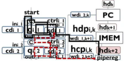
Setup constraints mean that input data of registers must be stable before writing to registers. Figure 3 represents paths related to setup constraints. sdpi,l (solid line)
rep-resents a data-path from sdi_1 to the destination register
pipereg where data is written through the source mem-ory IMEM. scpi,l (dotted line) represents a control path
fromsdi_1 to the destination registerpipereg through the control modulectrli_2. tminscpi,l,tmaxsdpi,l,tsetupk, and
smi,lrepresent the minimum delay ofscpi,l, the maximum
delay ofsdpi,l, the setup time for the destination register
pipereg, and the margin for tmaxsdpi,l. The setup con-straint can be represented by the following equation:
tminscpi,l> tmaxsdpi,l+tsetupk+smi,l (1)
If this constraint is violated, we need to adjust the delay elementsdi_1orsdi_2.
There are two types of sdpi,l. One is a forward path
where the source register is controlled by a previous con-trol module as shown in Fig.3(a) and the other is a back-ward path where the source register is controlled by a next control module as shown in Fig.3(b). We define local cycle timelcti and global cycle timegct. The local cycle time
lctiis defined for each pipeline stageiin which is equal to
the maximum delay ofscpi,l,tmaxscpi,l, in pipeline stage
i. The global cycle timegctis the maximum lcti for all
lcti. The global cycle time with input data interval decides
the throughput of asynchronous pipelined processors.
Figure 4: Data-pathhdpi,k and control path hcpi,k for a
hold constraint.
Figure 5: Forward path cf pi_1 and backward pathcbpi_1 for a control initialization constraint.
Hold constraints mean that input data of registers must be stable during writing to registers. Figure 4 represents paths related to hold constraints. hcpi,k (dotted line)
rep-resents a control path from sdi_1 to the destination reg-ister pipereg where data is written. hdpi,k (solid line)
represents a data-path from sdi_1 to the destination reg-ister pipereg through data-path resources. tminhdpi,k,
tmaxhcpi,k,tholdk, andhmi,k represent the minimum de-lay ofhdpi,k, the maximum delay ofhcpi,k, the hold time
for the destination register pipereg, and the margin for
tmaxhcpi,k. The hold constraint can be represented by the following equation:
tminhdpi,k > tmaxhcpi,k+tholdk+hmi,k (2)
If this constraint is violated, we need to adjust the delay elementhdk.
Control initialization constraints mean that the initializa-tion of control modules must be completed after the control signal by the assertion ofouti_jreaches to the next control
module. Otherwise, the assertion is disabled. Figure 5 rep-resents paths related to a control initialization constraint.
cf pi_1(solid line) represents a control path fromsdi_1to
ci_2. cbpi_1 (dotted line) represents a control path from
sdi_1toci_2 throughqi_1. tmaxcf pi_1 represents the max-imum delay of cf pi_1 and tmincbpi_1 represents the min-imum delay of cbpi_1. cmi_1 represents the margin for
tmaxcf pi_1. The control initialization constraint can be rep-resented by the following equation:
tmincbpi_1 > tmaxcf pi_1+cmi_1 (3)
Figure 6: The maximum delays of two control pathsscpi,l
andscpi+1,lmust be nearly equal to each other in
simulta-neous writing constraints.
Simultaneous writing constraints mean that all of regis-ters must be written to the same timing. In pipelined cir-cuits, the throughput depends on the global cycle timegct. Therefore, to delay all of register writing timing until the global cycle time does not affect the throughput. In ad-dition, as a difference of register writing timing may lead to setup/hold violations, to preserve these constraints re-duces the occurrence of setup/hold violations. On the other hand, to satisfy simultaneous writing constraints results in behaviors like synchronous circuits. Different from syn-chronous circuits where global clock signals are used, reg-isters are controlled by different control modules in this cir-cuit model. Therefore, we expect low power consumption for designed asynchronous processors even though these constraints are preserved. Figure 6 represent two control pathsscpi,l(dotted line) andscpi+1,l(solid line) for setup
constraints. These constraints can be represented by the following equation:
tmaxscpi,l 'tmaxscpi+1,l'gct (4)
If the above relationship is violated, we adjust delay ele-mentssdi_2andwdi_2,kfortmaxscpi,land delay elements
sdi+1_2, andwdi+1_2,kfortmaxscpi+1,l.
3
Field programmable gate array
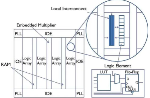
Field Programmable Gate Array (FPGA) is one of recon-figurable devices. FPGA has been used in many embedded systems because of the advantage such as lower design cost and flexibility to change circuit structure. Figure 7 shows the structure of Altera Cyclone IV FPGA.
The FPGA consists of Logic Array Blocks (LABs), Em-bedded Multipliers, Random Access Memories (RAMs), Input/output Elements (IOEs), and Phase Locked Loops (PLLs). A logic array consists of 16 logic elements (LEs). A logic element consists of a D Flip-Flop (DFF) and a 4-to-1 Look Up Table (LUT). Any logic function with four inputs can be implemented on an LUT based on a Static
Figure 7: Structure of Altera Cyclone IV FPGA [10].
RAM. Most of commercial FPGAs has the similar struc-ture like this FPGA.
We use two primitives in Altera FPGAs. One is LCELL and the other is DLATCH. LCELLs are used to implement delay elements such assdi_j and DLATCHes are inserted
after C-elements to carry out static timing analysis cor-rectly with the initialization of C-elements. Both of them are mapped to LUTs.
4
Design of asynchronous processor
on commercial FPGAs
In this section, we describe the proposed modeling method and design flow. Even though we target Altera FPGAs in this paper, as there is a similar design environment, we think that we can design asynchronous processors on other FPGAs such as Xilinx FPGAs with the modification of the proposed modeling method and design flow.
4.1
Modeling method
As shown in Fig.2, bundled-data implementation used in this paper consists of a control circuit and a data-path cir-cuit. We use the same data-path resources as the ones used in synchronous circuits. Therefore, we mainly describe modeling of the control circuit.
The proposed modeling method extends the method de-scribed in [11] where FPGAs are not considered. Initially, pipeline stages are modeled by a Finite State Machine (FSM) where nodes represent a pipeline stage and edges represent a control flow between pipeline stages. Figure 8(a) represents an FSM for a 5 stage pipelined processor. IF, ID, EX, MEM, and WB represent instruction fetch from the instruction memory, instruction decode, execution, data memory access, and write back to the register file.
Figure 8: Modeling flow of control circuit: (a) FSM and (b) generation of a control circuit from FSM.
Figure 9: Internal structure of control modules.
fromouti_j toci_j are inserted. In the modeling, we just
insert delay elementssdi_j which consist of one LCELL.
All other delay elements are inserted during delay adjust-ment after synthesis because other delay eleadjust-ments are re-quired when timing constraints such as hold constraints are violated.
Resisters and memories are triggered byacki_jof
corre-sponding control modules. We insert a glue logic to regis-ters and memories to generate a local clock signal for them fromacki_j and other conditional signals generated from
the data-path circuit.
Figure 9 shows the structure of ctrli_j for Altera
Cy-clone IV FPGA. There are two DLATCHes in a ctrli_j.
One is after the C-element ci_j and the other is after the
C-element in the Q-moduleqi_j. They are used to initialize
the output of C-elements and to execute static timing analy-sis correctly. Delay elementssdi_j,hdk,cdi_j, andwdi_j,k
consist of LCELLs. They work as buffers. To avoid renam-ing of the output signals of delay elements by the synthe-sis tool Altera Quartus Prime, we assignsynthesis_keep
commands to the output signals of delay elements. Note that we need to avoid logic optimization of control mod-ules and all of delay elements by Quartus Prime. If they are optimized after synthesis by Quartus Prime, we need re-synthesis by assigningdesign_partitioncommands to control modules and delay elements.
Finally, we prepare two models of the bundled-data
im-Figure 10: Verilog HDL models of an asynchronous pro-cessor: (a) simulation model and (b) synthesis model.
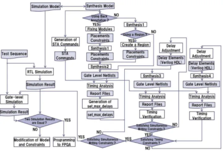
Figure 11: Proposed design flow.
plementation by Verilog Hardware Description Language (HDL) which is a standard modeling language for FPGAs. The first model is for Register Transfer Level (RTL) simu-lation before synthesis and the latter model is for synthesis. As RTL simulation does not allow to involve primitive cells DLATCHes and LCELLs, we represent them using logic expressions. Figure 10 (a) and (b) represent the simulation model and the synthesis model forqi_j in control module
ctrli_jusing Verilog HDL.
4.2
Design flow
The proposed design flow uses the design environment Al-tera Quartus Prime. To design asynchronous processors with bundled-data implementation on commercial FPGAs, we need to consider timing analysis, constraint generation, and delay adjustment for asynchronous processors which are not supported by the design environment.
Figure 11 represents the proposed design flow to imple-ment asynchronous processors on Altera FPGAs. The in-puts of the design flow are the simulation model and the synthesis model of an asynchronous processor.
correctly by TimeQuest Timing Analyzer in the Quar-tus Prime, we generate report_timing commands and
report_path commands. report_timing commands are used to analyze path delays between registers to ob-tain setup and hold times tsetup and thold for registers.
report_pathcommands are used for other paths. Note that Altera recommends us to set start and end points of paths with primary inputs, registers (flip-flops and latches), and primary outputs. On the other hand, most of paths related to timing constraints in the bundled-data implementation starts or ends by other pins or nets through registers. For example,sdpi,lstarts from the output ofsdi−1_2to the des-tination register through the source register. In such cases, we divide paths into sub-paths and preparereport_timing
andreport_pathcommands for divided sub-paths. For ex-ample ofsdpi,l, areport_pathcommand is prepared to
an-alyze from the output ofsdi−1_2to the source register and a
report_timingcommand is prepared to analyze from the source register to destination register.
In the design flow, we synthesize bundled-data imple-mentation without any constraints at first (Synthesis1). Then, we decide whether we generate placement con-straints or not. There are two possibilities to generate placement constraints. First is to fix the locations of placed resources in the first synthesis (Back Annotate). Second is to prepare a region to place logics of a given processor model (Create a Region). If we use the placement con-straints, we carry out the second synthesis (Synthesis2). From the static timing analysis result for the first or sec-ond synthesis, we analyze the global cycle timegctof the synthesized circuit. Then, we generate the maximum path delay constraints for all paths with the global cycle time
gctso that the global cycle time of iterative synthesis re-sults closes togct. Then, with the generated constraints, we repeat synthesis and static timing analysis (STA) until simultaneous constraints are satisfied (Synthesis3). Then, we repeat synthesis and and STA until all other timing straints are satisfied (Synthesis4). If some of timing con-straints are violated, we carry out delay adjustment for cor-responding delay elements. Finally, through the gate-level simulation for the synthesized processor, we program the synthesized processor on the target FPGA. In the rest of this sub-section, we describe the generation of constraints and the approach for delay adjustment.
4.2.1 Generation of design constraints
Generation of the Maximum Delay Constraints.We as-sign the maximum delay constraints to all paths related to setup constraints usinggctobtained from the STA re-sults by TimeQuest Timing Analyzer in Quartus Prime with
Figure 12: Generation of the maximum delay constraints.
report_timingandreport_pathcommands.
From the STA results, first, we analyze local cycle time lcti for each pipeline stage and global cycle time
gct. Second, we decide the margin smi,l for tmaxsdpi,l. Third, we decide two parameters scpmargin and dif f.
scpmargin represents a margin between tmaxsdpi,l and
tminscpi,l. Largerscpmarginmay result in that setup con-straints seem to be satisfied easily. However, it degrades the performance of the synthesized processor because it may lengthengctafter the third synthesis. dif f represents the difference betweentmaxscpi,landtminscpi,l.
The maximum delay constraints forscpi,l,tconstcp, are
calculated by the following equation.
tconstcp=gct (5)
The maximum delay constraints forsdpi,l,tconstdp, are
calculated by the following equation.
tconstdp=tconstcp−scpmargin−dif f−smi,l (6)
As same asreport_timingandreport_path, we assign the maximum delay constraints to sub-paths ofscpi,land
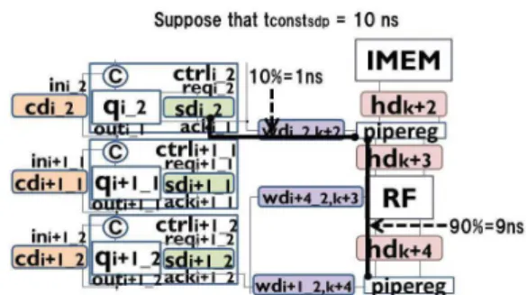
sdpi,lif these paths include several registers. From the STA
results, we decide the ratio of delay for each sub-path. For example, suppose thattconstdpforsdpi,lin Fig.12 is 10 ns
and the ratio of delay from sdi_2 to the source register is 10% oftmaxsdpi,lobtained from STA. Then, the maximum delay constraint fromsdi_2to the source register becomes 1 ns and the maximum delay constraint from the source register to the destination register becomes 9 ns.
We use set_max_delay commands to represent the maximum delay constraints. We prepare a Synop-sys Design Constraint (SDC) file which includes all of
set_max_delaycommands.
Generation of Placement Constraints. There are two approaches to generate placement constraints. The first ap-proach is to make a region for placement. In the first syn-thesis report (Synsyn-thesis1), we can get the information about the number of used logic elements. From the number of logic elements, we decide a region of FPGA. The region is created by usingLogicLockin Quartus Prime.
ap-Figure 13: Effect of placement constraints: (a) based on a region and (b) based on the back annotation.
proach, we assignLogicLockfor each resource (i.e., data-path resources such as registers and control modules) in the synthesis model (Fixing Modules). Through the first syn-thesis with placement constraints byLogicLock, we back annotate the locations of used logic elements, pins, multi-pliers, and memories in the first synthesis result to a con-straint file using Quartus Prime. The locations of resources are represented byset_location_assignmentcommands in the constraint file.
As the second approach fixes the locations of the logic to the first synthesis result, it may reduce the number of delay adjustment. However, it may worse performance if more delay elements are required because the placed logic may affect the placement of newly introduced LCELLs for delay elements. On the other hand, the first approach may allow to place newly introduced LCELLs so that they can be placed freely inside the region. However, it may increase the number of delay adjustments. Figure 13(a) and (b) rep-resent placed logics in the target FPGA when the first and the second approaches are used.
4.2.2 Delay adjustment
From the static timing analysis (STA) result with
report_timing andreport_path commands, simultane-ous writing constraints are checked. For a given margin
gctmarginfor the global cycle timegct,sdi_j orwdi_j,k
are adjusted so that all of tmaxscpi,l are within gct ±
gctmargin. sdi_j is adjusted if all oftmaxscpi,l are out ofgct±gctmarginwhilewdi_j,kis adjusted if only
cor-responding tmaxscpi_j,l is out of gct ±gctmargin. We generate Verilog HDL models for adjusted delay elements. Figure 14 represents an example of delay adjustment for simultaneous writing constraints.
Next, we adjust setup, hold, and control initialization constraints. As the adjustment ofhdk affects tosdpi,l, we
adjust hold constraints at first and then we adjust setup
Figure 14: Delay adjustment for simultaneous writing con-straints.
straints reflecting the added or removed delay forhdk to
sdpi,l. The adjustment ofcdi_jdoes not affect to the paths
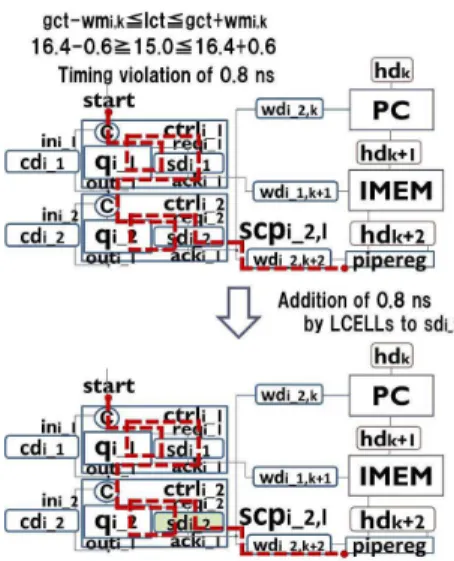
related to setup and hold constraints. Therefore, there is no order for delay adjustment between setup (hold) constraints and control initialization constraints. From the STA result usingreport_timingandreport_pathcommands, we as-sign the delays to both left side and right side of in the inequalities (1), (2), and (3) (see Section 2). By the sub-traction of the right side value from the left side value, we add LCELLs to corresponding delay elements to satisfy the constraint if the subtraction result is a negative value (i.e., a timing violation). On the other hand, we remove LCELLs from corresponding delay elements if the left side value is larger than the right side value plus the marginscpmargin. Although that the left side value is larger than the right side value means no timing violation, the large left side value results in that gctbecomes a large value. Therefore, we remove LCELLs if the left side value overs the right side value plusscpmargin. Figure 15 represents an example of delay adjustment for setup constraints.
After we generate Verilog HDL files for adjusted delay elements are generated, we repeat synthesis, STA, and de-lay adjustment until all of timing constraints are satisfied.
5
Experiments
5.1
Experimental results
Figure 15: Delay adjustment for a setup constraint.
Figure 16: Block diagram of the MIPS processor in [12].
data memory access, and write back). The asynchronous MIPS processor supports 9 instructions (lw, sw, j, beq, add, sub, or, and, slt).
We compare the designed asynchronous MIPS proces-sors with the synchronous MIPS processor in terms of area, execution time, dynamic power consumption, and energy consumption. The used synthesis tool and simulation tool are Altera Quartus Prime ver.15.1 and ModelSim-Altera ver.10.4b. TimeQuest timing analyzer in Quartus Prime is also used to analyze path delays. The target device is Altera Cyclone IV (EP4CE115F29C7).
Initially, we synthesize the synchronous MIPS proces-sor "Sync" by changing clock cycle time so that the clock frequency is maximum. The clock cycle time of "Sync" is 16 ns. Then, we design three asynchronous MIPS proces-sors. "Async1" is the one without placement constraints. "Async2" is the one that the asynchronous MIPS proces-sor is placed inside a region represented by a placement constraint. "Async3" is the one that the locations of all used resources are fixed to the same locations as the first synthesis in the design flow. Table 1 represents parame-ters for three asynchronous MIPS processors. We decide
LEs, (b) the number of LUTs, and (c) the number of regis-ters (DFFs).
Figure 18: Execution time of MIPS processors: (a) multi-plication and (b) matrix multimulti-plication.
gctmargin,smi,scpmargin, anddif f from the STA
re-sults for the first and second synthesis. gctis the value obtained by the STA result for synthesized circuit where all timing constraints are satisfied.
Table 2 represents the number of delay adjustments for three MIPS processors. "Simul" and "Others" represent the number of delay adjustments for simultaneous writing constraints and other timing constraints such as setup con-straints.
Figure 17 represents the area of the MIPS processors. Figure 17(a), (b), and (c) represent the number of used LEs, LUTs, and registers (DFFs). These are reported by Quartus Prime. Comparing to "Sync", the increase of LUTs and registers in three asynchronous MIPS processors is less than 5%. However, the number of LEs is increased 25% for "Async1", 54.5% for "Async2", and 54.0% for "Async3". This is because LUTs and DFFs are separated to different LEs even though an LE has one LUT and one DFF.
Figure 18 represents the execution time obtained by gate-level simulation after the designs using ModelSim-Altera. We prepare two test benches, (a) a multiplica-tion and (b) a matrix multiplicamultiplica-tion. In both cases, com-pared to "Sync", the execution time is increased 12.5% for "Async2" and 18.8% for "Async3" and decreased about 13.8% for "Async1". This is because the global cycle time of "Async2" and "Async3" is increased and the global cy-cle time of "Async1" is decreased compared to the cycy-cle time of "Sync" (see Table 1).
Table 2: The number of delay adjustments.
name Simul Others
Async1 3 0
Async2 6 0
Async3 3 0
Figure 19: Dynamic power consumption of MIPS proces-sors: (a) multiplication and (b) matrix multiplication.
the other hand, compared to "Sync", the dynamic power consumption of "Async2" and "Async3" is reduced 19.4% and 15.3% for the multiplication and 18.9% and 14.2% for the matrix multiplication. As dynamic power consumption depends on frequency which is a reciprocal of the clock cy-cle time, the longer global cycy-cle time results in the lower dynamic power consumption. On the other hand, the dy-namic power consumption caused by the global clock sig-nals (Clock in Fig.19) is reduced in all of asynchronous MIPS processors.
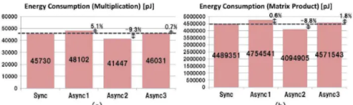
Figure 20 represents the energy consumption which is obtained by the product of execution time and dynamic power consumption. Compared to "Sync", in both multipli-cation and matrix multiplimultipli-cation, the energy consumption is increased 5.1% and 0.6% for "Async1" and 0.7% and 1.8% for "Async3". On the other hand, compared to "Sync", in both multiplication and matrix multiplication, the energy consumption is reduced 9.3% and 8.8% for "Async2".
5.2
Discussion
The experimental results show that the proposed model-ing method and design flow generate two possibilities of asynchronous processors on commercial FPGAs. First it to generate a high performance asynchronous processor like "Async1". As the global cycle time is smaller than the shortest clock cycle time, it increases throughput. To gen-erate the high performance one, we should rely on
com-Figure 20: Energy consumption of MIPS processors: (a) multiplication and (b) matrix multiplication.
Table 3: Ratio of dynamic power consumption ([%]).
name test bench block routing
Async1 multiplication 47.4 52.6
matrix multiplication 46.9 53.1
Async2 multiplication 52.3 47.7
matrix multiplication 50.9 49.1
Async3 multiplication 46.8 53.2
matrix multiplication 46.3 53.7
mercial design environment without placement constraints. Second is to generate a low energy asynchronous processor like "Async2". To generate the low energy one, we should prepare a region to place the logics of processors.
In all of three asynchronous processor designs, there is no big difference for the number of delay adjustments. On the other hand, interestingly, to satisfy simultaneous writ-ing constraints may reduce the possibilities of other timwrit-ing violations.
cessors. Comparing with a synchronous MIPS processor, one of them reduced the global cycle time which results in 13.8% performance improvement and another one reduced the energy consumption 9.3% for a multiplication and 8.8% for a matrix multiplication.
In our future work, we are going to reduce the number of used logic elements to reduce the dynamic power con-sumption of routing resources. In addition, we are going to design different asynchronous processors to generalize the proposed method.
Acknowledgement
This work is partially supported by Grant-in-Aid for Sci-entific Research from Japan Society for the promotion of science (#15K00080).
References
[1] A. Putnam et al., "A Reconfigurable Fabric for Ac-celerating Large-Scale Datacenter Services", Proc. ISCA’14, pp.13–24, 2014.
[2] M. Tranchero and L. M. Reyneri, "Exploiting syn-chronous placement for asynsyn-chronous circuits onto commercial FPGAs", Proc. FPL, pp.622–625, 2009.
[3] Q. T. Ho et al., "Implementing Asynchronous Circuits on LUT Based FPGAs", Proc. FPL, pp.36–46, 2002.
[4] H. Saito et al., "A Floorplan Method for Asyn-chronous Circuits with Bundled-data Implementation on FPGAs", Proc. ISCAS, pp.925–928, 2010.
[5] K. Takizawa et al., "A Design Support Tool Set for Asynchronous Circuits with Bundled-data Implemen-tation on FPGAs", Proc. FPL, pp.1–4, September 2014.
[6] Nikolaos Minas et al., "FPGA Implementation of an Asynchronous Processor with Both Online and Of-fline Testing Capabilities", Proc. Async, pp.128–137, 2008.
[7] Jens Sparso and Steve Furber, "Principles of Asyn-chronous Circuit Design: A Systems Perspective", Springer, 2001.
[8] F. U. Rosenberger et al., "Q-Modules:Internally Clocked Delay Insensitive Modules", IEEE Transac-tion of Computer, vol. C-37, no.9, pp. 1005-1018, 1988.
[11] S. Iwasaki, "Design and Evaluation of a Low Power Asynchronous AVR Processor considering a Cycle Time Constraint", Master Thesis, the University of Aizu, 2014.