S
AN
L
UIS
O
BISPO
C
OLLEGE OF
ENGINEERING
D
EPARTMENT OFE
LECTRICALE
NGINEERINGRF Power Amplifier
Authors
A
NDREWF
ERGUSONA
NGELD
ELGADOR
ACHANONW
AJANAKUNAKORNAdvisor
D
R. D
EANA
RAKAKIAbstract
Wireless devices are part of everyday life, cellphones and radio receivers impact more people than any piece of technology. Thus, the respective building blocks continue to advance and achieve better performance. A primary component of all wireless communication systems is the power amplifier that drives the antenna. The Institute of Electrical and Electronics Engineers (IEEE) holds the International Microwave Symposium (IMS) every year where teams compete internationally for the most efficient RF Power Amplifier (PA). Power amplifier technologies strive to maximize efficiency and linearity. Topologies to consider are D, E, F, F-1 and Doherty
since they have a maximum theoretical efficiency of 100%. This project focuses on the design and simulation of a power amplifier in which design is optimized for Power Added Efficiency (PAE) at 3.5GHz using the class F topology and it will use IMS competition rules and performance metrics. Power conversion efficiency from DC to RF is referred to as PAE and linearity is the maximum spur to fundamental power ratio. An ideal class F amplifier creates a square output drain voltage and a half wave rectified sinusoidal current in order to maximize efficiency. For this project, a 3.5GHz GaN HEMT based power amplifier is designed and simulated in Keysight Advanced Design System (ADS) and Momentum [1]. Load-pull simulation, including the transistor model, sweeps the load impedance to find the optimal load for maximized efficiency or power output. An input and output microstrip stub network can be designed to match these ideal impedances to a 50Ωline. Momentum, an ADS integrated EM simulation software, is used
CONTENTS
I Introduction 3
II Design Specifications 3
III Topology Selection 3
III-A Class A Amplifier . . . 3
III-B Class AB, B, and C Amplifiers . . . 3
III-B1 Class B . . . 4
III-B2 Class AB . . . 4
III-B3 Class C . . . 4
III-C Class F/F-1 Amplifier . . . . 4
III-D Doherty Power Amplifier . . . 5
IV Component Selection 6 IV-A Transistor Selection . . . 6
V Class F Amplifier Design 6 V-A Bias Point Selection . . . 6
V-B Load Pull Simulation . . . 6
V-C Matching Network Design . . . 7
V-C1 Input Network . . . 7
V-C2 Output Network . . . 8
VI Simulation Results 9 VI-A EM Simulation . . . 9
VI-A1 Input Network . . . 9
VI-A2 Output Network . . . 10
VI-B Harmonic Balance Amplifier Simulation . . . 11
VII Results 13
VIII Improvements/Future Endeavors 13
References 13
Appendix A: Figures 14
I. INTRODUCTION
Power Amplifier (PA) topologies F, F-1, and Do-herty all exhibit 100% theoretical efficiency. The amplifier topology chosen in this design is a Class F because it enables a high efficiency for constant power signals such as the one used for determining the amplifier’s figure of merit. This is only achieved when infinite harmonics are controlled to create a square-wave drain voltage and half-wave sinusoidal drain current. Theoretically the transistor dissipates zero power since there is always either zero voltage across the transistor or zero current through the transistor at all given time.
PAE is calculated by,
P AE = Pf und−Pin
Pdc
(1)
where Pfund, Pin, and Pdc are the output power at
the fundamental frequency, input power, and power supplied by the DC source respectively.
In practice, designs only control up to the third harmonic since it reduces complexity and compo-nents. Designs that control up to fifth harmonic are rarely used since the performance improvement for effort involved is too small to justify.
II. DESIGNSPECIFICATIONS
The specifications for the power amplifier are set primarily to comply with the International Mi-crowave Symposium High Efficiency Power Ampli-fier Student Design Competition rules. The figure of merit (FoM) used in the competition is defined by,
F oM =P AE∗ffund0.25 (2)
where ffund is the fundamental frequency.
The power amplifier specifications are outlined in Table I. The decision of 3.5GHz as the fundamental frequency is due to component availability at that frequency. To compete with previous competition
TABLE I: Given design parameters
Parameter Value Unit
Fundamental Frequency 3.5 GHz Power Added Efficiency >80 % Carrier to Intermodulation Ratio >30 dB
Input Power 27 dBm
Output Power 40 dBm
Number of Ports 2 –
Number of DC Rails 2 –
winners outlined in Figure 1, a minimum PAE of 80% must be achieved. Maximum input power and allowable output power are 27dBm and 4-40W (36dBm-46dBm) respectively. The chosen transis-tor, CG2H40010F CREE HEMT, limited the output power to 10W, or 40dBm. Transistor selection is discussed in section IV.
Fig. 1: Previous IMS Contest Winners
III. TOPOLOGY SELECTION
Topology selection parameters include efficiency, linearity, and design complexity. Brief descriptions of common amplifier topologies are given below.
A. Class A Amplifier
Class A amplifiers are the simplest topology. The amplifier consists of a single transistor in a common-emitter configuration with its base or gate biased to maintain the transistor in the on state. This corresponds to a conduction angle of 360°. Since the output is a scaled version of the input wave, this technique ensures a highly linear amplifier. Un-fortunately, due to constant conduction through the transistor, class A amplifiers suffer from undesirable maximum theoretical efficiency of 50%.
B. Class AB, B, and C Amplifiers
Fig. 2: Theoretical Amplifier Topology Efficiencies [3]
1) Class B: The bias point for a Class B ampli-fier is set such that only half of the input waveform turns on the transistor. Therefore, the output current waveform is a half-wave rectified sine wave. This bias point increases the efficiency to a maximum theoretical value of 78.5%, but maintains the same output power capability as a class A amplifier. This effect is shown in Figure 4. However, the lower conduction angle causes signal distortion. Figure 3 shows the affect of conduction angle on signal distortion. In general, as the conduction angle decreases, the ratio of power at the fundamental frequency to power in the harmonics also decreases. Due to decrease in linearity, but increase in effi-ciency, there is a trade-off between choosing class B over class A.
Fig. 3: Harmonic Power in Amplifier Output Signal due to Decreasing Conduction Angle [6]
2) Class AB: Class AB amplifiers use a bias point between class A and class B. This results in a improved linearity but decreased efficiency relative to class B. This trade-off can be acceptable depending on the application. Class AB maximum output power can be greater that a class A, as shown in Figure 4. This could be useful in a power optimized design.
3) Class C: The bias point in a class C amplifier reduces the conduction angle to less than 180°. Once again, this increases efficiency but results in severe signal distortion, hence this amplifier topology is unsuitable for linear amplification applications. In addition to the linearity issue, the output power decreased significantly at low conduction angles (see Figure 4). Although it is theoretically possible to reach 100% efficiency with a class C amplifier, this is not realizable, since conduction angles very close to 0° will result in no output power.
Fig. 4: Theoretical Amplifier Topology Output Power and Efficiency [6]
C. Class F/F-1 Amplifier
To improve upon the efficiency of class A-C amplifiers, class F and F-1 apply waveshaping to
but the voltage waveform requires an overdriven transistor and an additional output network design. By overdriving the transistor into its knee region, voltage output will no longer be linear with respect to transistor current as seen in Figure 5. Thus, distortion will occur in the signal, producing power at the harmonic frequencies of the fundamental.
Fig. 5: Ideal Transistor Knee Region [5]
Fig. 6: Theoretical Drain Voltage (Red) and Current (Blue) Waveform
Since the square wave is composed of odd harmonics the waveform is shaped by an output network with appropriate impedances at each har-monic. For class F, even harmonics must be very low impedance to ground (shorted) and the odd harmonics must be presented with a high impedance (open). At frequencies less than 1GHz lumped ele-ments are used. However, at frequencies exceeding 1GHz (3.5GHz design frequency), transmission line based circuits minimize footprint and improve wave shaping performance. This project focuses on class F amplifier design; detailed information contained in section V.
In an ideal class F amplifier, a theoretical 100% PAE is possible due to no power dissipation in the transistor. However, to obtain this theoretical PAE, the load must control an infinite number of harmonics and all non-transistor components must be lossless. In practice, class F designs are tuned up to the 3rd or 5th harmonic; the 5th providing
mini-mal improvements compared to design effort. One consideration is the parasitic drain-source capaci-tance which will short relatively high frequencies to ground, thereby limiting wave shaping control. As a result, typical class F applications have efficiencies in the 80% range. Figure 7 shows a basic class F schematic with 3rd harmonic control. The second LC network resonates (open circuit) at the funda-mental frequency f0, shorting all other harmonics to
ground. The first LC network at the collector output resonates at the 3rd harmonic 3f
0. This results in
only odd harmonics at the drain.
Fig. 7: Simplified Third Harmonic Lumped Element Class F Amplifier Schematic
D. Doherty Power Amplifier
A major issues with all previously mentioned classes is that they are designed and biased for one specific input power. Their operating performance degrade outside of a small range of powers. Many modern wireless communication protocols include a variable input amplitude over time. A Doherty amplifier aims to fix this issue by implementing two separately biased transistors that work together to amplify a wider range of input powers. One transistor is always on and amplifies the low power components of the signal and one transistor that amplifies the peak power regions. Doherty ampli-fiers can have better efficiency ratings in many real world applications than class F/F-1. Since IMS2020
IV. COMPONENT SELECTION
A. Transistor Selection
The CG2H40010 transistor excelled in three main metrics in comparison to other transistors manufac-tured by CREE: Power rating, operating frequency at maximum efficiency, and cost. Table II lists the viable transistors manufactured by CREE that met the competition criteria. The CG2H40010 has the highest efficiency at a power rating within the design criteria with the added advantage of having an ADS model from CREE and being available for free sampling. There are several advantages to this transistor which make it the ideal selection for the design. For one, the Gallium Nitride (GaN) on Silicon Carbide (SiC) structure of transistors manufactured by CREE maximize power density and minimize package size and parasitics. Thus, this transistor is more suitable for high frequency applications.
TABLE II: Transistor Selection Table
Transistor Max Efficiency at Power Max
Operating Frequency Frequency
CG2H40010 72% Eff @ 3.7GHz 10W 6GHz CGH40006S 65% Eff @ 2.0GHz 6W 6GHz CGH40006P 65% Eff @ 2.0GHz 6W 6GHz CG2H40025 72% Eff @ 3.8GHz 25W 6GHz CGH40035F 68% Eff @ 3.7GHz 35W 4GHz
To produce a 180° conduction angle, an initial bias point is chosen using the transistor model in DC simulation. Results are shown in Figure 8. The selection is at a point where the input signal can overdrive the transistor.
Fig. 8: Drain Current vs. Drain-Source Voltage over Various Gate Voltages
Figure 9 shows the test circuit used to simulate and adjust values of gate and drain biasing for Figures 8 and 10.
Fig. 9: FET Test Circuit Schematic
Fig. 10: Drain Current vs. Gate-Source Voltage over Various Drain Voltages
Figure 10 shows the drain current with respect to gate bias. Observe the region around VGS=−2.9V
where the FET is in the boundary of conduction.
V. CLASSF AMPLIFIERDESIGN
A. Bias Point Selection
The first step in the design process is to select a bias point for the transistor. The transistor bias point of −2.8V Vgsmaximizes efficiency, maximizes
output power, and ensures 180° conduction angle. Both class F and class B use identical bias point selection methods. A gate bias voltage of −2.8V is near the cutoff point on the Id vs. Vgsplot in Figure
10, which ideally results in a 180° conduction angle.
B. Load Pull Simulation
Fig. 11: Load Pull Analysis Displaying Maximum PAE Load Impedance
Fig. 12: Load Pull Analysis PAE & Output Power Contours
The drain voltage is set to the data sheet rec-ommended 28V, and bias voltage to −2.8V as de-termined by the previous harmonic-balance sim-ulations (Figure 8) for class F operation. Input power is set to 27dBm and fundamental frequency to 3.5GHz. For this specific simulation, the only sweep parameters available are the load impedance at the fundamental frequency and harmonic fre-quencies individually. As seen in Figure 11, the harmonic frequency load values can be set to pre-determined values while one of them is swept at a time. The real and imaginary min/max values to sweep can be set using theZ real min, Z real max, Z imag min, Z imag max respectively. Increasing the number of ZL points (Z real num points and
Z imag num points in Figure 11) and narrowing
the sweep range will increase accuracy and reso-lution, but also simulation time.
Results are displayed in contours on theΓL plane
which outline the impedances required to achieve a specific PAE or output power as seen in Figure 12. Load pull simulation variants also include bias point sweeps and can be performed for both single and two-tone signals that will determine a preferable bias point.
Since the source impedance is specified as one of the simulation parameters, an iterative simulation method is employed. The steps for this design technique are as follows:
1) Set source impedance to 50Ω.
2) Set gate bias to -2.8V, set drain bias to 28V,
Pavs dBm to 27.
3) Set a large enough sweep range to see contours on any location in the smith chart.
4) Simulate and move black mPdel vs PAE Rho
marker to point of maximum PAE. 5) Record input impedance.
6) Use conjugate of the recorded input impedance as the new source impedance.
7) Repeat steps 4 through 6 until improvement between iterations is negligible.
Figure 13 shows the resulting data from the final load pull analysis at the mPdel vs PAE marker. Expected PAE, Power Delivered, and target load impedance are 83.2%, 40.7W, and 6.42 + j5.26 re-spectively. The load and input impedance specified are the target impedances for both the input and output networks of the amplifier.
Fig. 13: Load Pull Amplifier Characteristics at 83% PAE
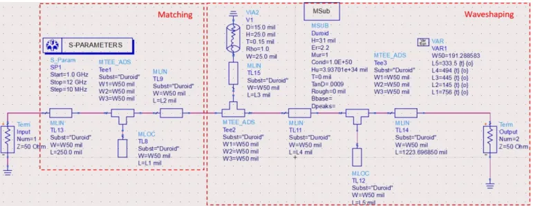
C. Matching Network Design
1) Input Network: To avoid reflections at the input and maximize PAE, the input network must match the 50Ω termination to the desired source
Fig. 14: ADS Input Network
previously. The second and third harmonics created by the transistor are filtered from the transistor gate to maintain a sinusoidal input, containing only the fundamental frequency. In order to design a network that both filters and matches, the filter is designed first by creating a stub filter with a matched S22 at
the harmonics. After that, the network should match the targetΓL to 50Ωby first translatingΓLacross the
filter network. This design procedure can be done using a Smith chart and a simple single stub tuning method.
Due to the matched impedance at the 2nd and 3rd harmonics (7GHz and 10.5GHz), seen from the tran-sistor gate, S22 is minimized at those frequencies, as
seen in Figure 15, while achieving the target source impedance at the fundamental.
Fig. 15: ADS Input Network |S22|
2) Output Network: Output network design is similar to the input network. The goal is to simul-taneously control the impedances presented to the drain of the transistor at the fundamental frequency, and the second and third harmonics. The waveshap-ing network in Figure 16 ensures the correct loads at the harmonics.
Fig. 16: Amplifier Output Waveshaping Network
In Figure 16, the CG2H40010F transistor will re-place Term1 and the matching network will rere-place Term2. TL5 is λfund/4 at the fundamental, which
presents an open and short circuit impedance to the transistor at the fundamental and second harmonics respectively. A voltage source can be connected in parallel with the capacitor, DC Block1, to provide the VDS bias to the circuit.
Fig. 17: Amplifier Output Network
circuit stub at the third harmonic, which rotates to a short circuit across at the length of the stub. This then rotates 3λ3rd/4 (third harmonic) across TL1 and
presents an open circuit to the transistor.
The fundamental impedance is not set to ZL
by the waveshaping network, so a matching work is required. The single stub matching net-work is placed after the waveshaping netnet-work so that the fundamental impedance can be moved without affecting the second and third harmonic impedances. The network will match the 50Ω load
to an impedance, ZA shown in Figure 17, which
becomes ZL when it is translated back across the
waveshaping network. The first step to design this is to determine the required ZA. This is done by
translating ZL across TL1 and TL6 in Figure 17
toward Term2. A single stub matching network is then designed on a Smith chart to match the 50Ω
load to the calculated ZA. The Smith chart design is
shown in Appendix A, Figure 33. The waveshaping network and matching network are shown together in Figure 17.
Fig. 18: Tuned Output Network Schematic
After the initial design is completed on the Smith chart, it is implemented in an ADS schematic using microstrip lines. The electrical lengths from the Smith chart design are converted to physical lengths using the ADS LineCalc tool. The schematic is
then tuned using the ADS tuning tool. The tuned schematic is shown in Figure 18.
VI. SIMULATIONRESULTS
A. EM Simulation
Electromagnetic (EM) simulations analyze the physical structure of a design to calculate the s-parameter response. ADS includes an EM simula-tion module, Momentum, which analyzes the input and output network layouts. The EM simulation is set up to include the board stack-up as seen in Figure 19, input and output ports, and the frequency plan.
Fig. 19: EM Simulation Layer Stack-up
Fig. 20: EM Simulation Port Editor
In order to simulate accurate port connections, the
port editor defines reference impedance (50Γ), port
layer (Conduction Layer), and feed type (TML). Through testing we found that feed type affects results significantly. The transmission line (TML) feed type most closely approximates ADS piece-wise simulation.
Fig. 21: Input Network Layout
placed on the top side in order to avoid coupling between the first two stubs since EM simulation includes radiation and coupling effects.
Once S-Parameters are generated, the S22 (Figure
22) and impedance values are compared in Table III. Figure 22 compares ADS piece-wise simulation (red) against Momentum results (blue) from 0 to 8.5GHz. The impedance match is close to the target
ΓS at the fundamental, however the network no
longer filters at the 3rd harmonic as seen in the magnitude plot.
Fig. 22: EM (red) and piece-wise (blue) Simulation Input Network |S22|
TABLE III: ADS vs. Momentum Source Impedance Results
ADS Momentum
1.85 - j11.79 1.52 - j13.11
Discrepancies between Momentum and ADS sim-ulations can be attributed to the 62mil thickness. Via length from signal to ground introduce sig-nificant phase shift for frequencies above 8.5GHz. Changing a single via property, height, diameter, or metal thickness, in the short circuit stub has drastic results on the S22 response. Momentum simulations
account for physical dimension effects to result in accurate network design
2) Output Network: The output network is also simulated in Momentum. EM simulations confirm the ADS model. First, a layout is generated from the ADS schematic, as shown in Figure 23.
Fig. 24: Amplifier Output Network Momentum vs. ADS S11 Response
Fig. 23: Amplifier Output Network Layout
The S11 response is plotted on a Smith chart and
is shown in Figure 24
Markers on the ADS and Momentum traces show S11 locations at the fundamental, second, and third
Fig. 25: Harmonic Balance Simulation with Microstrip Components
Fig. 26: Drain Voltage FFT, Class F Amplifier with Microstrip Components
B. Harmonic Balance Amplifier Simulation
The Harmonic Balance (HB) simulation in con-junction with an S-parameter simulation verifies the amplifier design and operation while providing final efficiency and gain values.
The schematic in Figure 25 includes the entire amplifier design with microstrip components as ob-tained in Matching Network Design, section V-C. The DC bias point for the transistor gate and drain is −2.8V and 28V, respectively. The bias point was selected in section V-A. Figure 26 confirms the output network design of a short at the second harmonic for the drain voltage. Figure 27 displays a short at the third harmonic for the drain current.
Fig. 27: Drain Current FFT, Class F Amplifier with Microstrip Components
Fig. 28: Drain Voltage and Current Time Domain, Class F Amplifier with Microstrip Components
Fig. 29: Amplifier |S21| at ffund, −2.8V Gate Bias
Fig. 30: Amplifier |S11| at ffund, −2.8V Gate Bias
harmonic magnitude to be 13 of the fundamental. Figure 26 shows a fundamental and third harmonic magnitude of 16.5V and 4.0V, respectively, a ratio of 14. Furthermore, since the drain current should reflect a half-wave rectified sinusoid, the drain cur-rent’s second harmonic should be proportional to the fundamental by 34π ≈ 0.424. Figure 27 shows fundamental and second harmonic magnitude of 1.65A and 0.35A, respectively, for a ratio of only 0.212. Since harmonic control includes up the third harmonic and the third harmonic does not meet expected values, addition tuning is required.
Power probe components in ADS detected an input power of 236mW, less than the 500mW (27dBm) provided by the input signal. This leads to S-parameter simulations which justify the input
Fig. 31: Amplifier |S21| at ffund, −3.1V Gate Bias
Fig. 32: Amplifier |S11| at ffund, −3.1V Gate Bias
power discrepancies.
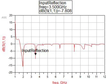
Figure 29 displays amplifier |S21| values of port 1 as the input and port 2 as the load. Figure 30 displays amplifier input reflection |S11|. At the
op-erating frequency of 3.5GHz, an |S11| of −2.413dB
represents 57.3% reflected power. This justifies the input power difference noted in HB simulation. Fig-ure 29 displays an amplifier |S21| plot. At 3.5GHz,
the simulated gain is 16.7dB, greater than the desired minimum gain of 13dB. Interestingly, the forward gain peak (and subsequently decrease in input reflection) is located at 3.48GHz.
Gate bias adjustment to −3.1V resulted 80.78% efficiency and 15.913dB of forward gain (see Figure 31). This adjustment also yielded an |S11| local
VII. RESULTS
A power amplifier design comparable to IMS contest winners, requires minimum PAE and output power. Project results in Table IV show amplifier performance over a range of bias points. At −3.1V bias, PAE is 80.8%, just greater the 80% minimum. Power output is 9W (39.5dBm) which is well over the 4W (36dBm) requirement. A 15.91dB gain meets the 13dB minimum. The gate bias was revised from −2.8V to −3.1V. If system is redesigned at this revised bias level, improved performance could be attained.
TABLE IV: Power Amplifier Design Results
Gate DC Input Output
Bias Power Power Power Efficiency Gain
(V) (W) (mW) (W) (dB)
-2.8 11.613 236 9.127 76.56% 16.700 -2.9 11.325 242 9.081 78.05% 17.062 -3.0 11.057 249 9.041 79.52% 17.173 -3.1 10.826 256 9.001 80.78% 15.913 -3.2 10.654 263 8.951 81.55% 4.959
With these performance metrics, the figure of merit for this design is 110.5, exceeding all IMS contest winner from 2006 to 2014 (See Figure 1). However, while parasitics and physical characteris-tics dimensions were included in simulation, actual results might degrade if the design is fabricated and tested.
VIII. IMPROVEMENTS/FUTURE ENDEAVORS
The simulation results performed on this project were promising for a high performance RF am-plifier. However, design process refinements could improve results and ensure proper operation when fabricated.
It is recommended that future project teams opti-mize gate bias as the initial design step to maxiopti-mize PAE. While the −2.8V gate bias places the transistor in the knee region, this does not optimize efficiency and gain. Determining the optimal point improves overall system performance, as seen in Table IV.
The input and output network design could be improved in future projects. In this project, the input wave shaping network is designed to filter out all harmonics generated by the transistor. However, performance might be improved if the harmonics were shorted to ground instead of filtered. This
creates destructive interference at the transistor gate, and ensures only fundamental frequency power ex-ists at the transistor. Also, further input network tuning would improve input matching and reduce source input reflection. The output network match-ing performance at the third harmonic should be refined to produce the desired power ratio. This will improve efficiency by reducing overlap of voltage and current waveforms.
In addition to improving the design methodology, the design process could be improved by performing Momentum EM simulations earlier and more often. Tuning the physical layout, as opposed to schematic. The importance of this step was seen in the EM simulation of the output network that did not meet expectations.
Lastly, implementing this design in hardware will validate the design method, design process, and sim-ulations. The simulation results show an amplifier that meets all design requirements, but performance could be improved with further work.
REFERENCES
[1] Santa Rosa, CA, USA. Keysight.(2019) [Online]. Available: https://www.keysight.com/us/en/products/software/pathwave-design-software/pathwave-advanced-design-system.html, Accessed on: Feb. 12, 2020.
[2] G. Eason, B. Noble, and I. N. Sneddon, “On certain integrals of Lipschitz-Hankel type involving products of Bessel functions,” Philosophical Transactions of the Royal Society of London. Series A, Mathematical and Physical Sciences, vol. 247, pp. 529–551, April 1955.
[3] https://www.electronics-tutorials.ws/amplifier/amplifier-classes.html
[4] P. B. Kenington, High-linearity RF amplifier design. Milton Keynes, UK: Lightning Source UK Lts., 2010.
[5] https://www.electrical4u.net/electrical-basic/use-knee-point-voltage/
APPENDIXA
FIGURES
APPENDIX B
SENIOR PROJECT ANALYSIS
Project Title: RF Power Amplifier
Student Names: Andrew Ferguson Angel Delgado
Rachanon Wajanakunakorn
Advisor’s Name: Dr. Dean Arakaki
Summary of Functional Requirements
In order to fabricate a power amplifier that would be able to compete in the International Microwave Symposium, competition requirements needed to be met while meeting performance characteristics similar to previous competition winners. Therefore, this project required: minimum 13dB gain, 4-40W output power, 80% Power Added Efficiency, and -30dBc spur at minimum output power. In order to have access to components optimized to operate at our target frequency, the frequency of operation for this project was selected to be 3.5GHz.
Primary Constraints
The main constraint we needed to consider when deciding design requirements for an RF power amplifier was access to lab equipment which would be able to test at a high enough frequency. Most of the lab equipment we had access to could only support frequencies below 5GHz, constraining our frequency of operation. The second constraint we faced was the access to high power, high frequency transistors due to the high price point. In the end, we were constrained to a transistor that CREE could provide for free.
Economic Impact
Human Capital - The RF amplifier will create many jobs in engineering, manufacturing and sales. The group will hire engineers, sales people, and manufacturing technicians to assist in bringing the product to market. On top of the direct impact, the increased performance will allow a small boost in the industries that use it, creating even more secondary jobs.
Financial Capital - The increased performance of the RF power amplifier will draw customers from many industries. This will cause a large demand for the product, which will justify its high price. Therefore, the device will be very lucrative and create a lot of financial capital.
Natural Capital - The RF power amplifier uses semiconductor materials and printed circuit boards, which use harsh chemicals in manufacturing. These chemicals can cause negative effects if released into natural environments. The group will ensure proper use of chemicals and potentially produce circuit boards by milling instead of photolithography to cut down on chemical use.
Cost and Timing - While still in early development, initial cost targets have been made for the RF power amplifier. A cost of 1500USD will place the product in an aggressive sales position, with its list of engineering specs. In order to allow wholesale at this price, the product must be manufactured under 1000USD. Therefore, the cost of components will be tracked through development. The product is set to be sold in August of 2020. Therefore, development must be completed by June of that year.
If manufactured on a commercial basis:
Environmental
Since this project focused on simulation, environmental impacts only included electricity. The carbon footprint is dependant on the energy source. In 2018, California generated less than 1% of electrical energy from oil or coal. This further reduces the project’s environmental impact. However, if this project were to proceed to fabrication of boards, there would be environmental impacts related to that process:
What environment impacts are associated with manufacturing or use of the product?
The RF power amplifier has negative environmental impacts due to its use of semiconductors and printed circuit boards. However, current technology also uses these materials, so the addition of the RF power amplifier to the market will have no impact on the overall environmental burden of communication systems. On top of this, the RF power amplifier will excel in efficiency, which will save energy in these systems. This will have a positive impact on the environment.
Which natural resources and ecosystem services does the project (directly and indirectly) improve or harm?
The RF power amplifier uses semiconductors, which are mined materials. This places a burden on the environments surrounding these mines, and can negatively impact the ecosystem around it. However, these materials are very abundant on Earth and therefore, there is little risk of depleting the resource. The amplifier also requires electrical energy to run, which could be generated from a non renewable source. This can be fixed by using more renewable energy generation methods.
Does the project impact other species?
The RF power amplifier can affect the ecosystem of the areas around where the raw materials are mined. This can negatively impact plant and animal life in the area and reduce the biodiversity of an area if species are forced away.
Manufacturability
The RF power amplifier could be very easily manufactured using traditional printed circuit board techniques. The product would be simply developed and sold as a PCB, so would use a photolithography or milling process for board manufacturing and reflow soldering process for attaching components to the board. Much of this can be automated, decreasing the cost in the long term.
Sustainability
The RF power amplifier will be a very low maintenance component of a larger RF system. After initial integration, the amplifier should not need maintenance. If there is an issue with the device, the whole amplifier will be replaced, meaning that there is no direct maintenance. The amplifier should also be a reliable component since the base components that build up to it are all reliable.
The RF power amplifier impacts the sustainable use of resources because it uses raw materials which are non renewable such as semiconductors. While it does make use of these materials, current technology that the amplifier would replace also use the same materials. Therefore, there is no net effect on the consumption of non renewable raw materials. However, the amplifier will reduce the energy consumption of systems it is in, resulting in less energy resources being used.
The design on the RF power amplifier would be improved if it were designed to be more broadband than it currently is. While the amplifier will be very high performance compared to other competing designs, its usefulness is limited by the fact that it can only be used at a very specific frequency.
Ethical
While the applications for RF amplifiers most often include RF communication services for the public such as phone and radio services, private communications, and satellite communications, there are high frequency applications that can be borderline unethical. When the average individual thinks of wireless, they will probably think of our ability to communicate wirelessly through electromagnetic waves in space. However, they may not think about the side of wireless that actually causes damage to materials. On a small scale, microwaves essentially bombard your cold food with high powered 2.4GHz waves which so happens to be the same resonance frequency as water. This will cause the water molecules to vibrate and lead to a buildup of energy, and boiling. On a larger scale, a pulse of EM waves set off by a malicious individual can fry all electronics in a radius of the pulse. This is also known by the military as an EMP (Electromagnetic Pulse Attack). While wireless can be used in a safe and useful way, it can also be used for malicious attacks that can range from damage to people and properties.
One such example is the U.S government’s Active Denial System. This device uses millimeter waves with a short enough wavelength that it will not penetrate a person’s skin more than a 1/64th of an inch in order to radiate a ‘man-sized’ beam that will induce a burning sensation from a range of up to 1,000 meters that will instinctively cause crowds to move out of the way and disperse. While it is true that the waves at about 94GHz will not have the same effect as a 2.4GHz microwave oven on a person, the waves still literally cause people’s skin to burn immediately but the government claims that because the person will move out of the way instinctively, it is not a dangerous weapon. They also claim that any damage caused by this weapon is ‘reversible’, which can be said for just about anything but a 3rd degree burn. In the case of the Active Denial System, RF Power Amplifiers are being used in a way that we believe to be unethical and go against our moral values. We believe that while we cannot control the use of our product in these unethical applications, we will not sell or support and individual or company that comes into possession of one of our amplifiers.
Health and Safety
The health concerns surrounding out product ultimately come down to the customer use case and product application. While the direct use of our product cannot harm a person directly, it can be used to radiate signals which can be of concern to public safety. The power rating at which our amplifier will operate will only be harmful if used to transmit frequencies such as 2.4GHz while in direct proximity of the public. At max power (40W) this frequency could have harmful effects if not shielded correctly. One way companies avoid such effects is by modulating signals to different frequencies and keeping any transmitters far away from populated areas as well as directional shielding.
Social and Political
Depending on our market choice, there are political implications surrounding this product in regards to the governmental defense sector aid that it could provide. Selling this product to the government could tie our design efforts to any kind of action the military decides to use the amplifier for. Any direct or indirect action taken as an effect of a communications system or direct military weapon in which this device is used could be seen as our direct effort to strengthen the U.S military. However, any efforts towards the greater connectivity of our country as a whole with the goal of creating a more integrated society would therefore further our cause by introducing more efficient and powerful communication technology in order to help the U.S spearhead the next generation of mobile networking.
Development
![Fig. 2: Theoretical Amplifier Topology Efficiencies [3]](https://thumb-us.123doks.com/thumbv2/123dok_us/8219425.2179192/5.918.80.447.81.304/fig-theoretical-amplifier-topology-efficiencies.webp)
![Fig. 5: Ideal Transistor Knee Region [5]](https://thumb-us.123doks.com/thumbv2/123dok_us/8219425.2179192/6.918.86.442.256.532/fig-ideal-transistor-knee-region.webp)