LEABHARLANN CHOLAISTE NA TRIONOIDE, BAILE ATHA CLIATH TRINITY COLLEGE LIBRARY DUBLIN OUscoil Atha Cliath The University of Dublin
Terms and Conditions of Use of Digitised Theses from Trinity College Library Dublin
Copyright statement
All material supplied by Trinity College Library is protected by copyright (under the Copyright and Related Rights Act, 2000 as amended) and other relevant Intellectual Property Rights. By accessing and using a Digitised Thesis from Trinity College Library you acknowledge that all Intellectual Property Rights in any Works supplied are the sole and exclusive property of the copyright and/or other I PR holder. Specific copyright holders may not be explicitly identified. Use of materials from other sources within a thesis should not be construed as a claim over them.
A non-exclusive, non-transferable licence is hereby granted to those using or reproducing, in whole or in part, the material for valid purposes, providing the copyright owners are acknowledged using the normal conventions. Where specific permission to use material is required, this is identified and such permission must be sought from the copyright holder or agency cited.
Liability statement
By using a Digitised Thesis, I accept that Trinity College Dublin bears no legal responsibility for the accuracy, legality or comprehensiveness of materials contained within the thesis, and that Trinity College Dublin accepts no liability for indirect, consequential, or incidental, damages or losses arising from use of the thesis for whatever reason. Information located in a thesis may be subject to specific use constraints, details of which may not be explicitly described. It is the responsibility of potential and actual users to be aware of such constraints and to abide by them. By making use of material from a digitised thesis, you accept these copyright and disclaimer provisions. Where it is brought to the attention of Trinity College Library that there may be a breach of copyright or other restraint, it is the policy to withdraw or take down access to a thesis while the issue is being resolved.
Access Agreement
By using a Digitised Thesis from Trinity College Library you are bound by the following Terms & Conditions. Please read them carefully.
TW O -PH O TO N-ABSO RPTIO N
IN SEMICONDUCTOR
MICRO-CAVITIES
by
T o rs te n K ru g
A th esis s u b m itte d for a d eg ree of
D o c to r of P h ilo so p h y
in t h e U n iv e rsity of D u b lin
u n d e r t h e su p e rv isio n of
P ro f. J o h n F. D o n eg a n
School of P h y sics
T rin ity College D u b lin
'TRINITY COLLEGE' 1 5 MAY 2006
This thesis has not been subm itted as an exercise for a degree at any other university. The work described herein is entirely my own, with the exception of the assistance mentioned in the acknowledgements and the collaborative work noted in the publications.
I hereby agree th a t the Library may lend or copy the thesis upon request.
Acknowledgement
My appreciation to Herve Folliot, the originator of the work on tw o-photon ab
sorption in micro-cavities in this group. Herve Folliot designed the cavities used
in this research. Herve Folliot also provided the early modelling backup for this
project.
I would like to th an k all people who were p art of the Sem iconductor Photonics
G roup over the last couple of years.
This research would not have been possible w ithout the support and sam ples pro
vided by Sheffield University. I particularly want to th an k Geoff Hill and John
R oberts for providing the samples.
I would like to say special thanks to Prof. John Donegan for giving me the op
p o rtu n ity to join his research group and for providing resources for my work and
travel.
I am grateful to Dr. Louise Bradley for academic guidance, helpful conversations
over the last few years and m ost im portantly for accepting to proof read this
m anuscript.
Special thanks also to Paul M aguire and Dr. Liam B arry from D ublin C ity Uni
versity for great support in this collaboration. Paul, th an k you very much for all
the ’’black” boxes you drove back and forth.
Words of thanks go also to lots of other people.
To Dr. Vincent Weldon for proof reading this m anuscript and all th e help and
optim ism he pu t into the m aintenance of the O PO and Ti-Sapphire laser.
To Mick Lynch for his vast and sometimes confusing knowledge (well, it certainly
got me confused, m ost of the tim e) and technical expertise which led to so many
ideas and results along the way.
PhD student John O ’Dowd, over the final few m onths.
O utside of college, I th an k all my friends who contributed in th eir own ways to
this thesis. To Janka, Anna, Bocky, M atthias, B ettina, Roisin, M arg and Ralf.
Special thanks goes to the members of the
Schnickels
group for lots of interesting
conversations and many, many, many emails th a t provided essential com fort and
always rem inded me th a t there is also a life outside th e lab. On to p of th e list of
who I have to th an k how^ever is Irene, for all our good tim es th a t m ade th e last
two years a great time.
P u b lica tio n s and P resen ta tio n
”Two-Photon Absorption photocurrent enhancem ent in a bulk A lG aA s sem icon
ductor m icrocavity”, T .K ru g , H.Folliot, M.Lynch, A.L.Bradley, J.F.D onegan, L.P.Barry,
J.S .R oberts and G.Hill, presented a t Euroconference on Q uantum O ptoelectron
ics for NanoTechnology: U ltrafast Processes in Solid S tate N anostructures, Les
Houches, April 2002
”Two-photon absorption enhancem ent in AlG aAs microcavities”,
T.K rug, M.
Lynch, A.L.Bradley, J.F.D onegan, H.Folliot, L.P.Barry, J.S .R oberts and G.Hill,
presented a t 26th International Conference on the Physics of Semiconductors,
Edinburgh, July 2002
”Two-photon absorption enhancem ent in a I l l - V sem iconductor m icrocavity”,
T.K rug, H.Folliot, M.Lynch, A.L.Bradley, J.F.D onegan, L.P.Barry, J.S.R oberts
and G.Hill, presented at SPIE O pto Ireland: O ptoelectronic and Photonic De
vices, Galway, Septem ber 2002
’’Design o f micro-cavity sem iconductor devices fo r highly efficient optical sw itch
ing and sampling applications”,
L.P.Barry, P.M aguire, T.K rug, H.Folliot, M .Lynch,
A.L.Bradley, J.F.D onegan, J.S.R oberts and G.Hill, presented a t Laser and Electro-
O ptics Society (LEGS 2002), 15th Annual Meeting of the IEEE, Volume 2, pages
839-840, November 10-14, 2002
” Two-photon-induced photoconductivity enhancement in sem iconductor microcav
ities: A theoretical investigation”,
H.Folliot, M.Lynch, A.L.Bradley, L.P.Barry,
T.K rug, L.A .D unbar, J.H egarty and J.F.D onegan, J. O pt. Soc. Am. B., V ol.19,
No. 10, O ctober 2002
’’Optical autocorrelation using two-photon absorption in sem iconductor m icro
cavities”,
M.Lynch, T .K rug, H.Folliot, A.L.Bradley, L.P.Barry and J.F.D onegan,
presented a t Semiconductor and Integrated O ptoelectronics (SIOE 2003), Cardiff,
Wales, April 14-16, 2003
”A novel approach towards two-photon absorption based detectors”,
T.K rug, H.Folliot,
M.Lynch, A.L.Bradley, L.P.Barry, J.F.D onegan, J.S .R oberts and G.Hill, pre
sented a t Conference on Laser and Electro O p tics/Q u an tu m Electronics and Laser
Science Conference (C LEO /Q ELS 2003), Paper CTUG5 Technical Proceedings,
B altim ore, M aryland, USA, June 1-6, 2003
”High-sensitivity two-photon absorption microcavity autocorrelator”,
T .K rug, M.Lynch,
A.L.Bradley, J.F.D onegan, L.P.Barry, H.Folliot, J.S.R oberts and G.Hill, P h o to n
ics Technology L etters, IEEE, Volume 16, Issue 6, June 2004, pages 1543-1545
”Two-photon absorption based microcavity detector”,
T .K rug, M.Lynch, A.L.
Bradley, J.F.D onegan, H.Folliot, L.P.Barry, J.S.R oberts and G.Hill, presented
at Em erging Technologies in O ptical Sciences (ETO S 2004), Cork, Ireland, July
26-29, 2004
”Simulation o f a high-speed demultiplexer based on two-photon absorption in
semiconductor devices”,
P.M aguire, L.P.Barry, T.K rug, M.Lynch, A.L.Bradley,
J.F.D onegan and H .Folliot, O ptics Com m unications 249, pages 415-420, 2005
”All-optical sampling utilising two-photon absorption in semiconductor microcav
it y ”,
P.M aguire, L.P.Barry, T .K rug, M.Lynch, A.L.Bradley, J.F.D onegan and
H.Folliot, Electronic Letters, Vol.41, No.8, pages 489-490, April 2005
”Resonance tuning of two-photon absorption microcavities fo r wavelength-selective
pulse m onitoring”,
T .K rug, W .H .Guo, J .O ’Dowd, M.Lynch, A.L.Bradley, J.F.D onegan,
L.Barry, P.M aguire, H.Folliot, su b m itted to PT L
’’All-optical sampling based on two-photon absorption in a semiconductor micro
cavity fo r high-speed O T D M ”,
P.M aguire, L.P.Barry, T .K ru g , M.Lynch, A.L.Bradley,
J.F.D onegan and H.Folliot, presented a t O pto Ireland (SPIE Europe), Dublin,
Ireland, April 4-6, 2005
”Two-photon absorption microcavity detector fo r femtosecond and picosecond pulses”,
T .K ru g , M.Lynch, A.L.Bradley, J.F.D onegan, P.M aguire, L.P.B arry and H.Folliot,
presented a t O pto Ireland (SPIE Europe), Dublin, Ireland, April 4-6, 2005
”Beam propagation analysis in two-photon absorption microcavity devices”,
T.K rug,
M.Lynch, A.L.Bradley, J.F.D onegan and H.Folliot, presented a t O pto Ireland
(SPIE Europe), Dublin, Ireland, April 4-6, 2005
A b stract
C o n ten ts
1
In tro d u ctio n and T hesis O verview
4
1.1 Integrated O p t i c s ...
4
1.2 Sem iconductor O ptical S w itc h e s ...
5
1.3 O ptical Sampling O scillo sco p e...
6
1.4 O ptical Demultiplexer ...
6
1.5 O ptical Time Division M u ltip le x in g ...
7
1.6 N on-Linear O ptical E ffe c ts...
10
1.7 Thesis O v erview ...
14
2
T w o -P h o to n —A bsorption
16
2.1 In tr o d u c tio n ...
16
2.2 Tw o-Photon P r o c e s s e s ...
16
2.3 TPA and Nonlinear O p t i c s ...
18
2.4 TPA in III-V S e m ic o n d u c to rs ...
20
2.5 TPA in Bulk Semiconductors ...
21
2.6 T w o-Photon A bsorption P h o t o c u r r e n t ...
23
3
Transfer M atrix M eth od
25
3.1 In tr o d u c tio n ...
25
3.2 Electric F i e l d ...
25
3.3 Transfer M a tr ic e s ...
27
3.4 Time and Space Inversion ...
29
3.5 The Fabry-Perot Resonator ...
32
3.6 D istributed Bragg R e f l e c t o r ...
35
3.7 Absorption E n h a n c em e n t...
43
3.8 Final Comments
...
48
4
D ev ice Sim ulation
49
4.1 A Planar M icro cav ity ...
49
4.3
G ehrsitz M o d e l ...
55
4.4
F in e s s e ...
56
4.5
Dielectric M irror Spectral B a n d w id th ...
58
4.6
M icrocavity R e s o n a n c e ...
58
4.7
Penetration Depth in Bragg M irro rs ...
60
4.8
Finite Reflection A n g l e ...
65
4.9
M icrocavity M o d e ...
68
4.10 Final TPA Microcavity D e sig n ...
68
5 M easurem ents at 890 nm
72
5.1
In tr o d u c tio n ...
72
5.2
D e v i c e ...
72
5.3
Experim ental Set-up
...
73
5.4
Device C haracterization
...
74
5.5
Dynamic M easurements
...
77
6 M easurem ents at 1.55 //m
79
6.1
In tr o d u c tio n ...
79
6.1.1
D e v ic e ...
79
6.1.2 Device C h a r a c te r iz a tio n ...
82
6.1.3 Dynamic M easurements ...
87
6.2
A u to c o rre la tio n ...
91
6.2.1
In tr o d u c tio n ...
91
6.2.2 T h e o r y ...
92
6.2.3 S e n s itiv ity ...
94
6.2.4 P o la r is a tio n ...
96
6.2.5 C on clusion...101
7 OfF-axis O peration and A p p lication s
102
7.1
Off-axis O peration ... 102
7.1.2 E xperim ental S e t - u p ... 103
7.1.3 T h e o r y ... 105
7.1.4 Off-axis M e a s u re m e n ts ... 112
7.1.5 Tunable A u to c o rre la to r... 120
7.1.6 C onclusion ... 121
7.2 Depth-of-Focus S c a n ... 122
7.2.1 In tr o d u c tio n ... 122
7.2.2 Theory and Analytic M o d e l ... 122
7.2.3 Experim ental S e t - u p ... 125
7.2.4 Depth-of-Focus M easurement ...126
7.3 Spectral Pulse S lic in g ... 128
7.3.1 In tr o d u c tio n ... 128
7.3.2 Experim ental S e t - u p ... 129
7.3.3 Theoretical A n a l y s i s ... 130
7.3.4 Experim ental R e s u lts ... 131
7.3.5 D isc u ssio n ... 137
7.3.6 S u m m a r y ... 139
8 C onclusion and Future W ork
140
8.1 C o n clu sio n ... 140
8.2
Future W o rk ... 140
8.2.1 Double Resonance Microcavity
... 141
1
In trod u ction and T h esis O verview
T his chapter opens w ith a discussion of recent developments in optical commu
nications. The need for further development continues, especially in th e area of
all-optical signal processing and signal m onitoring. Two-photon absorption mi
crocavities have been proposed as devices suitable for perform ing these functions.
1.1
Integrated O ptics
As m entioned before, the solution was to use wavelength m ultiplexing a t the op
tical level. The basic idea is to use different optical carriers or colours to tran sm it
different signals along the same fiber. The bottleneck in these systems is how
ever still the use of electrical technology for m ultiplexing and demultiplexing,
signal am plification, transponders and regenerators. The last three applications
are commonly known as the 3R regeneration of the optical signal (re-shaping, re
tim ing, re-am plification) [7]. In order to m onitor or analyse the signals they still
have to be dem ultiplexed, electrically regenerated and then m ultiplexed again.
O ptical switching units in DWDM links such as optical cross connects and op
tical add-drop m ultiplexers are of growing interest for tran sp aren t networks. At
th e m om ent optical traffic is connected w ith the help of distribution panels and
large electrical cross-connects [3], b u t w ithin a few' years it will be necessary to
switch, a t least p a rt of the exploding d a ta traffic, using quickly reconfigurable
optical cross connects. In the long term the idea is to do all this work on an
optical level and create all-optical networks [8].
1.2
S em ico n d u cto r O p tical S w itch es
One of the main advantages cited for optical signal processing is the capability
of all-optical devices to switch in a tim e much shorter th a n th a t achieved by
electronic devices [3, 9]. In order to im plem ent these devices, how'cver, optical
m aterials with suitable properties are required. Much current research is aim ed at
developing optical m aterials for these applications. Ideally such m aterials should
have (i) a large non-linearity w ith an ultra-short response tim e, and (ii) an ab
sence of slow non-linear effects such as carrier generation and therm al effects.
A lthough much current work centers on organic m aterials [10, 11], it would be
very attractiv e to utilize sem iconductor m aterials because of their com patibility
w ith electronic com ponents and th eir potential applicability for optoelectronic
integrated circuits.
th e m ost significant optical signal processing tasks, the m onitoring of network
perform ance and the dem ultiplexing of d a ta is vital if future network design and
operation are to meet the growing demands. In order to carry out these func
tions a t the very-high d a ta rates (>100 G b /s per channel) anticipated in future
networks, it is evident th a t nonlinear optical effects, which are present in optical
fibres, sem iconductor devices and optical crystals, can be employed, as these oc
cur on tim e scales in the order of a few-femtoseconds (10“ ^^ s).
1.3
O ptical Sam pling O scilloscope
T he stan d ard m ethod used to characterise and m onitor optical com m unications
system s involves the use of a fast photodetector in conjunction w ith a high-speed
sam pling oscilloscope. The opto-electronic conversion process in the photodetec
to r places a lim it on the overall bandw idth of the m easurem ent available due to
the speed lim itations of current integrated electronic circuit design. At present
this lim its the m axim um d a ta rate of a single channel th a t can be accurately
analysed to around 40 G b /s [12, 13]. As the individual d a ta rates are expected
to exceed 100 G b /s by 2010, it is im perative to develop a new optical sam pling
technique which can accurately characterize and m onitor perform ance in future
ultra-high speed networks [14, 15]. Such technology will become essential to both
network designers and network operators for system developm ent and testing.
1.4
O ptical D em ultiplexer
channel. The receiver in such a hybrid W D M /O T D M system will have to first
filter the aggregate signal to isolate the single wavelength channel of interest and
then perform dem ultiplexing of the resulting high-speed O TD M signal to acquire
a num ber of lower d a ta rate electronic channels. The developm ent of a dem ul
tiplexing device, th a t is capable of sim ultaneous filtering and detection, will be
vital in future photonic com m unications systems [16].
1.5
O ptical T im e D iv isio n M u ltip le x in g
Due to th e continued growth of the Internet and the introduction of new broad
band services such as video-on-dem and and mobile telephony, there will be a need
to b e tte r exploit the enormous bandw idth th a t optical fibre provides in the net-
w'ork. The conventional m ethod employed by many network providers is to use
optical m ultiplexing techniques to increase the num ber of carriers per optical fibre.
The m ost common variant, W avelength Division M ultiplexing (W DM ), divides
up the optical spectrum into a large num ber of non-overlapping wavelength bands
and tran sm its each individual data-channel using a different wavelength over a
single fibre. To increase capacity in WDM netw'orks, new tran sm itter/receiv er
pairing (operating a t a diff'erent wavelength) can be added, b u t this is expensive.
An alternative is to increase the d a ta rate tran sm itted per channel, b u t this is
lim ited by the speed of electronics in current integrated circuits. A nother option
is to m ultiplex in the tim e dom ain instead of the wavelength domain.
spectral w idth [19].
An alternative technique, th a t pushes neither WDM nor OTDM to its limits,
is to combine th e two systems, to form a hybrid W 'D M /O TD M approach [20].
This approach uses OTDM to enhance the bandw idth of a num ber of WDM
wavelength channels by p u ttin g OTDM coding on top of the d a ta of the channels
provided by W DM. This results in a smaller num ber of channels operating at
much higher d a ta rates, and may overcome some of the problems associated w ith
pushing W'DM and OTDM to th e higher d a ta rates.
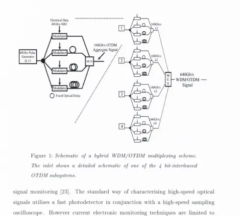
Figure (1) shows a layout for a hybrid W 'D M /O TD M network. It comprises of
4 bit-interleaved OTDM m ultiplexed systems [21], each operating a t a different
wavelength (Al, A2, A3, A4). A bit-interleaved OTDM system uses a train of
u ltra-sh o rt optical pulses to represent the d a ta in a single channel. To produce
the OTDM signal, a single pulse tra in is split into N copies by a passive coupler,
where N corresponds to the num ber of channels in the system (N = 4 in the
example show^n). Each pulse train is then subsequently encoded w ith d a ta from
an electrical source in an electro-optic m odulator. The m odulated pulse trains
then pass through a fixed fibre delay length, which essentially assigns each d a ta
channel to a specific bit slot in the overall multiplexed signal. The m ultiplexer
(MUX), a passive optical coupler, then combines the individual channels into a
single OTD M d a ta signal. The individual OTDM signals, each operating a t an
aggregate d a ta rate of 160 G b /s, are combined together in another passive optical
coupler to form the 640 G b /s hybrid d a ta signal.
In order to operate a t such high d a ta rates, future photonic networks will have to
carry out signal processing tasks, such as d a ta switching and perform ance moni
toring, in the optical domain. There is considerable interest in the developm ent
of new all-optical techniques to carry out perform ance m onitoring (sampling) and
d a ta switching (demultiplexing) w ithin the network [22].
Elcctrical Data 40Gb/s NRZ
l60Cib/sOTOM Aggregate Signab M odulator
4 0 0 h z Pulse G enerator
M U X M odulator
640Gb/s - W DM/QTDM —
Signal M odulator
Q Fixed Optica! Delay
F ig u r e 1: S c h e m a tic o f a h y b r id W D M / O T D M m u ltip le x in g s c h e m e . The in let sh ow s a d e ta ile d s c h e m a t ic o f one o f the 4 b it-in te r le a v e d O T D M s u b s y s te m s .
[image:20.536.31.522.50.492.2]1.6
N on -L in ear O ptical Effects
N on-linear optical effects, as m entioned above, which are present in optical fibres,
sem iconductor devices and optical crystals, occur on tim e scales in the order of
a few femto-seconds (10“ ^^s), and are therefore ideal for perform ance m onitoring
and high-speed optical dem ultiplexing of data. A num ber of industry leaders in
th e m anufacture of optical oscilloscopes [25, 26] are investigating the use of Second
Harm onic G eneration (SHG), an u ltrafast optical nonlinearity, for sam pling a t
higher d a ta rates. This involves combining a high-power optical pulse tra in to
the d a ta signal being analysed and generating the mixing product of b o th signals
in th e optical crystal. The energy of the mixing product pulse represents the
am plitude of the d a ta signal th a t can be detected by a slow photodetector. This
technology is used in two comm ercially available OSOs from Agilent (86119A)
and ANDO (AQ7750). U nfortunately there are a num ber of disadvantages in
using th e SHG process. These include:
• Very high optical intensities are required for the sam pling pulse due to poor
efficiency of the SHG process
• Stability problems associated wdth the use of free-space optics
• Need for phase m atching a t different wavelengths
O ne such n o n h n e a rity is T w o -P h o to n A bso rp tion (T P A ) in sem iconductors. T P A is a n o n lin ear o p tical-to -electrical conversion process w here two p h o to n s are a b so rb ed in th e g en eratio n of a single electron-hole p air. It occurs w hen a p h o to n o f energy h u is incid ent on th e active are a of a sem ico nd ucto r device w ith a b an d g ap E g > h v b u t less th a n 2 h u . U nder these conditions, incident p h o to n s do no t possess sufficient energy to pro du ce an electron-hole pair. However an electron- hole p a ir can be p ro duced by th e in sta n ta n e o u s ab so rp tio n of tw o p ho to ns, w here th e su m m a tio n of th e ind ividu al p h o to n energies is g re a te r th a n th e b an d gap. T h e g en era ted p h o to c u rre n t is p ro p o rtio n a l to th e square of th e intensity, an d it is th is n o n lin ear response, com bined w ith its u ltra -fa st response tim e of th e o rd er of 10“ ^^ s a t 1550 nm , th a t enables th e use of T P A for high-speed o p tical d em u ltip lex in g an d m o nitoring.
T h e m ain efficiency problem associated w ith T P A h as been overcom e by incor p o ra tin g a F ab ry -P ero t m icro-cavity into th e design of th e sem icon du cto r device [30, 31]. C h a ra c te risa tio n of these sem ico nd uctor devices an d ex p erim en tal re su lts, w hich are presen ted in th is work, have shown en h an cem en t of over four ord ers of m a g n itu d e in th e T P A p h o to c u rre n t by using a m icro-cavity stru c tu re . T h is allows for o p e ra tio n using o p tical in ten sities ty p ically found in an o p tical co m m u n icatio n netw ork. G iven th e increased non linear efficiency of T P A (due to th e m icro-cavity design), and th e fact th a t th e T P A process is u ltra -fa st, it is highly o p p o rtu n e to develop o p tical d em ultip lexers an d sam p ling oscilloscopes using th is novel an d innovative technology for use in fu tu re high-speed o p tical netw'orks.
O TD M channels, passes through a variable optical delay, which ensures th a t the
sam pling pulses arrive at the TPA detector at a tim e corresponding to the bit
slot of the signal to be m onitored. As there are four different vv^avelengths in the
hybrid signal, the sam pling pulse is scanned across each of the four (red, green,
blue, yellow) signal pulses in the bit slot of interest. The sam pling delay is pro
vided by generating the sam pling pulse a t a frequency slightly detuned from a
sub-harm onic of the high-speed b it-rate.
Variable Delay Sampling | | | |
Pulses Hybrid WDM/OTDM Signal 10:90 Coupler Hybrid With Sampling Pulse Continue Across Network Sampled Signal
M M
TPA Micro-CavityF ig u re 2; S c h e m a tic o f possible sa m p lin g s e t- u p in h y b rid W D M / O T D M n e tw o r k w ith T P A m ic r o c a v ity de te c tor.
on a constant background. Experim ental work carried out suggests th a t, w ith
th e current microcavity device, it is possible to successfully sample a d a ta pulse
w’ith duratio n less th an 2 ps a t d a ta rates in excess of 160 G b /s and w ith optical
peak intensity less th an 8 mW [32, 33].
1.7
T hesis O verview
The research described in this thesis is a continuation of the collaborative work
between th e School of Physics in T rinity College Dublin, the Research In stitu te
for Networks and C om m unications Engineering at Dublin City U niversity and
th e L aboratoire de Physique des Solides, INSA in Rennes. To build upon the
original work done in our group the aim was (i) to investigate the tw o-photon
absorption microcavity devices operating a t 1.55 //m, (ii) to investigate alignm ent
tolerance aspects of the device stru ctu re, (iii) to measure the sensitivity of the
device as a detector and (iv) integrating the device into a tw o-photon absorption
autocorrelator. Aspects of the tw o-photon absorption m icrocavity device which
had previously not been investigated include its efficiency and the ability to tune
th e resonance wavelength when illum inated w ith an off-normal incident beam .
The work carried out and described in subsequent chapters is sum m arized below.
C h ap ter 2 contains a discussion of the theory of Tw o-Photon A bsorption (TPA).
A basic introduction is given as well as an explanation of TPA in semiconductors.
This chapter also gives an analytical expression for the calculation of th e TPA
photocurrent in a microcavity device.
C h ap ter 3 deals w ith an explanation of the Transfer M atrix M ethod (TM M ),
by which a complete model of the m icrocavity device can be achieved. P a rts of
the model are outlined with some simple examples of their im plem entation. The
mechanism of absorption enhancem ent in a microcavity is described and an ana
lytic expression for the enhancem ent factor for single and tw o-photon absorption
is given.
Finally, different optical characterizations of microcavities are investigated, in
cluding the microcavity mode, microcavity resonance, finite reflection angle and
p en etratio n depth into the Bragg mirrors.
C h ap ter 5 is concerned with prelim inary experim ental and numerical results using
a proof-of-concept device working a t 890 nm. This chapter contains a description
of th e experim ental setup used and gives a full device characterization.
C h ap ter 6 contains the investigations into the tw o-photon absorption m icrocavity
devices working a t 1.55 /im. In Section 6.2 experim ental and numerical results
are presented on the sensitivity of a TPA autocorrelator.
In C h ap ter 7 the case of off'-axis operation is explained and analysed in Section
7.1 using diff'erent models. The im plem entation of the wavelength tu n ab ility
in a TPA autocorrelator is also proposed in Section 7.1. Experim ental results
th a t su p p o rt the numerical results are presented. In Section 7.2 depth-of-focus
m easurem ents using the TPA device are presented. To prove the suitability of
the TPA m icrocavity for sonogram applications initial m easurem ent in spectral
pulse slicing have been carried out and are presented in Section 7.3.
2
T w o -P h o to n -A b so r p tio n
2.1
In tro d u ctio n
R ecently, T w o -P h o to n -A b so rp tio n (T P A ) in sem ico nd ucto r devices has becom e
an a ttra c tiv e , inexpensive and convenient way to perform a u to c o rre la tio n m ea
su rem en ts of picosecond an d sub-picosecon d laser pulses. Since th e first d em o n
s tr a tio n of a u to c o rre la tio n using th is tech niqu e [34], m any com m ercially available
devices in different m a teria ls have been exam ined. T h is work has resu lted in high
sen sitiv ity c h a ra cterizatio n of sh o rt o p tical pulses using T P A based a u to c o rre la
to rs [35 — 51]
In a d d itio n to a u to co rrelatio n , m ore recent work has d e m o n stra te d th e p ossib ility
of using th e u ltra -fa s t T P A n o n lin earity for carry in g o u t high speed o p e ra tio n s
such as o p tical d em u ltip lex in g an d sam p ling for use in u ltra -h ig h cap acity o p tical-
tim e-d iv isio n -m u ltip lex ed (O T D M ) system s [52]. T his work used co m m ercial 1.3
//m laser diodes for T P A of 1.55 f i m signals [53, 54, 55], an d showed th a t th is tech n iq u e is prom ising for developing high speed com p on en ts for fu tu re T b i t/s
op tical system s.
How'ever, T P A devices still require high o p tical in p u t in ten sities in o rd er to get
a significant level of p h o to c u rre n t an d to exceed th e d o m in an t, resid ual lin ear
a b so rp tio n . O ne way of increasing th e T P A sensitivity is of course to use longer
activ e len gth s b u t th is is a t th e expense of speed w hich could p revent its use
in O T D M system s [38]. A n o th er app ro ach th a t has been proposed [56] is to
use a sem icon ductor m icrocavity w here th e length en h an cem en t can be achieved
artificially by th e use of a F a b ry -P e ro t cavity.
2.2
T w o -P h o to n P r o cesses
T h e first discussion of tw o -q u an tu m processes in th e in teractio n betw een electro
[57] in 1929 and in a later article [58] in 1931 th a t sum m arized the results of her
d octoral dissertation. In these studies, th e interaction of th e atom and th e field
were treated fully quantum mechanically using second-order p ertu rb atio n theory.
The concept of tw o-photon processes was used soon afterw ards to explain the
decay rate of m etastable atom ic states via tw o-photon spontaneous emission [59].
The probability of such spontaneous tw o-photon transitions was found to be much
sm aller th an those of allowed one-photon transitions by a factor of the order of
1/137 (1/137 Z Y
where 1/137 is an approxim ation for the fine stru ctu re constant
and
Z
is the atom ic num ber [60]. O bservation of TPA and stim ulated emission
processes however required the invention of the laser, which could produce inten
sities high enough to increase the tw o-photon transition probability to detectable
levels.
exper-im ent was carried out [65], because the Erbium doped Calcium Fluoride crystal
possesses a center of inversion and therefore second-harm onic generation should
be forbidden.
There have been many subsequent observations of tw o-photon absorption in m any
different m aterials and for a wide range of applications such as biological m aterials
[10, 11] and laser spectroscopy [66].
2.3
T PA and N onlinear O ptics
Tw o-photon absorption results in a transition of electrons th a t arises from th e
addition of the energy, m om entum and the angular m om entum of two photons.
Thus TPA is a non-linear optical-to-electrical conversion process. W hen th e tra n
sition considered is from the valence band to the conduction band of a semicon
ductor, the energy sum m ust be >
Eg, where
Eg is th e sem iconductor bandgap.
For degenerate TPA the two photons have the same energy
hu, we thus have
'2hu >
Eg .Here
h is the Planck constant and
v
is th e light frequency. In this
work only degenerate or quasi degenerate TPA will be considered, using ju s t one
light source, a t either around 900 nm or 1.55 /im.
in TPA experiments (duration, spatial fluctuations, coupling efficiency ...) [68].
Comparison between bulk and QW semiconductor structures is rather difficult
[69], and the use of either will depend on the anisotropy, speed, material growth
quality and TPA enhancement considerations. The TPA enhancement for a bulk
microcavity structure will be discussed later (in Section (3.7)).
One method of measuring TPA in semiconductors is to measure the attenuation
of the beam or pulse propagating through a two-photon absorbing medium. If
the pulse irradiance is /, then the pulse is attenuated according to the expression
Here
ct
is the single-photon absorption coefficient and (3
is the two-photon absorp
tion coefficient. If the thickness of material considered is much greater than the
wavelength of the light used for the measurement, internal reflections and inter
ference can be neglected. Neglecting the multiple reflections within the medium,
the transm itted irradiance is given by the expression
U r T
=
( 1 - i ? ) ^ / ( r , 0, ^)
^ ’ ’ ^
1 + /3 ( 1 - i ? ) / ( r , 0 , ^ ) ( l - e - “ ^ ) / a ‘
^ ’Here
L is the thickness and
R is the reflectivity of the medium. The TPA coeffi
cient
13
is related to the two-photon transition rate per unit volume
by
the
expression
p ■ (3)
electric field am plitude
E{f , uj )
is determ ined by the solution to M axwell’s wave
equation given by
(4)
Here
e
is the linear dielectric tensor, c the vacuum speed of light,
f
the position
m om ent per unit volume [35].
2.4
T PA in III-V Sem iconductors
In sem iconductors it is possible to have tw o-photon absorption from a single light
pulse w ith frequency
u
if twice the photon energy,
2hi',
exceeds the sem iconductor
energy gap
Eg,
Figure (3). The num ber of two-photon transitions per unit volume
per un it tim e
is given by second-order p ertu rb atio n theory as [35]:
From E quation (6) and (7) it is clear th a t the TPA tran sitio n rate depends on the
square of the light intensity. Here
n
is the index of refraction of the sem iconductor,
c is the vacuum speed of light, m is the electron mass,
e
is the electron charge,
h
is the Planck’s constant divided by
2tt,
and
I
is the power per unit area of
the laser radiation. The sum m ations are extended over all final states (or bands)
denoted by the index / and all interm ediate states denoted by th e index
i.
The
ground sta te is denoted by the subscript
g,
and the transition rate should be
averaged over this index if there is more th an one possible initial state. T he unit
vector d is directed along the electric field of the laser, and
pfi
and
pig
are m atrix
elem ents of the m om entum operator between the final state and th e interm ediate
vector along the light propagation axis and
P
is the nonlinear source dipole
X]
2a;)
where
P f i ■ ® P i g ' ^ ^ig ^
state and the interm ediate state and the ground state respectively. The angular
frequencies
ujg
and
cuig
correspond to the angular frequency differences between
the final state in the conduction band and the ground state in the valence band,
respectively. These differences, in general, depend on the wave vector
k. If the
tran sitio n rate is now expressed in term s of the peak electric field am plitude
E
instead of the irradiance
I, the transitio n rate per unit volume becomes
h
\2mLuJ
j
P / i ■ ® P i g ' ® 4 I . , , , , I I ,
5{hujfg — 2hui).
(7)
tlU Jia — tiCOIn addition to the p ertu rb atio n theory calculation of
th a t involves m atrix
elem ents between the initial and final unperturbed states, it is also possible to
calculate the transition rate by a m ethod th a t includes th e effect of the electro
m agnetic field on th e Bloch wave functions a t the beginning of th e calculation
[70].
2.5
T P A in B u lk S em ico n d u cto rs
For simplicity the following consideration is only done for two bands, th e valence
band and the conduction band as shown in Figure (3)
\'alence band; p orbitals (odd sym m etry) at the Brillouin zone centre
C onduction band: s orbitals (even sym m etry) at the Brillouin zone centre
The tran sitio n element
Sji
represents the num ber of possible transitions from the
initial sta te
i to the final state / in a semiconductor b an dstru ctu re [71]. The
tran sitio n elem ent
Sfi can be described as
\
E , - E , - h u ,
<*>
Energy
C onduction Band
ht)
k electron wavevector
V alen ce Band
Figure 3: TPA band structure.
mixing between the bands. Only w ith increasing electron wavevector the TPA
process also increases. This simple model does not take excitonic effects or non
parabolic bands into account.
[image:33.535.39.522.46.785.2]2.6
T w o -P h o to n A b so rp tio n P h o to c u r ren t
If b o th coefficients, a for single-photon absorption and
P
for tw o-photon absorp
tion, are considered the differential equations for intensity propagation
I{z)
in a
sem iconductor along the
2-axis is^ - r v T ( ^ \ - R T ( v ^ ‘^
dz
Solving for
I{z)
gives [74]
Now th e single-photon absorption and tw o-photon absorption contributions to
th e to ta l absorption can be found to be
IZ' = /O ( l - 9 ^ ) ^
(11)
and
tT P A - t ( i _ ^ ( '1 9 ')
° V
C ) a L + l n C
^
’
with
C = l + { P I o / a ) { l - e - ^ ^ ) ,
(13)
where
L
is the
length of the sem iconductor along the
2-axis.It is now assumed
th a t all the photon energy is used in creating electron-hole pairs w ithin the semi
conductor, the
quantum efficiency of the photoconductivity
is therefore 100%.
The resulting photocurrent
J
is then given by the following expression
where .4 is the illum inated area on the device (semiconductor). T hus, the two-
photon absorption response is lim ited by the single-photon absorption a t low
intensities and by the to ta l absorption in the sem iconductor on the high-intensity
side:
Here
I
indicates the light intensity for the dynam ic range shown in Figure (4).
a (cm )
100
10
“Dynamic Range
10
’^10
®Intensity
(W/m")
[image:35.536.43.518.65.789.2]3
Transfer M atrix M eth o d
3.1
In tro d u ctio n
T h e aim o f th is chapter is to provide a background to th e theo retica l m eth o d
used to characterize th e o p tical properties o f the m icrocavity structure. Since a
ty p ica l d ielectric cavity co n sists o f perhaps over 50 different layers, it is no longer
p o ssib le to express th e local electro -m a g n etic field in th e ca v ity a n a ly tica lly as
a fu n ction o f th e incident field. T h e standard technique is to use m atrices to
relate th e electric and m agnetic fields on one side o f a d ielectric boundary to
th e sam e qua n tities on th e other side. T h e standard m eth o d o f m atrices can be
used to ca lcu la te th e reflectivity and tran sm ission o f th e m icrocavity as w ell as
th e field in ten sity throughout th e structure [75, 76, 77, 78, 79]. T he m atrices
are based on a scalar plane-w ave solu tio n to M axw ell’s eq u ation s th a t relate
th e incident and o u tg o in g electric field w hen at an interface. T h is chapter w ill
b e organized along th e follow ing lines: Section (3.2) gives the electric field wave
eq uation . Sections (3.3) and (3.4) show th e im p lem en ta tio n o f th e transfer m atrix
m eth o d . In S ection s (3.5) and (3.6) th e F abry-P erot resonator and th e d istrib u ted
B ragg reflector are discussed respectively. W ith th a t background Section (3.7)
gives a description o f th e absorption enhancem ent o b tain ed using a m icrocavity
structure.
3.2
E lectric F ield
In th is chapter a structure m ade o f a stack o f different sem icon d u ctor layers o f
given thicknesses and infinite lateral ex ten sio n is considered. T h e w h ole structure
is therefore planar and tran slation invariant along th e plane. T h e a x is perp en d ic
ular to th e plane is labelled as th e 2 axis. T h e layers are assum ed to be m ade o f hom ogen eou s m aterials w ith uniform , frequency independent d ielectric co n sta n ts
field E a t frequency uj, in th e absence of charge or c u rren t den sity [p = 0, j = 0), th e M axwell eq u atio n for th e electric field m ay be w ritte n as [79]
o;2
V E{ r , z) + — e { z ) E{ f , z) = 0, (16)
C2
w here r is th e p o sitio n vector in th e plane a n d e{z) is th e d ielectric c o n s ta n t profile. A ccording to th e assu m p tio n s m ade earlier, th e fu n ctio n e{z) is piece- wise c o n stan t. In ad d itio n , it is assum ed to vary only w ith in a finite 2 in terv al, w hich m eans th a t th e thickness of our m ultilayer s tru c tu re is finite. B ecause of th e in p lan e tra n s la tio n a l invariance, th e solutions of E q u a tio n (16) are plane weaves along th e in-plan e direction. For each given in -p lan e wave vector k\\ an d p o la risa tio n th e electro -m agn etic field can be w ritte n as
(17)
w here is th e p o la rizatio n vector. R e s u b stitu tin g into E q u a tio n (16) gives a one d im ensional hom ogeneous second ord er differential eq u atio n for th e m ode fu n ctio n Uj^^^Jz):
^(z)
^ 2 + { e { z ) - 4 ) U , ^ ^ J z ) = 0. (18)
T h is eq u atio n m ay be sep arately solved for each hom ogeneous layer. For a layer w'ith dielectric co n stan t e th e m ode fun ction ^{z) can be expressed as
+ E , { h ) e ‘' " \ (19)
w here
T h e so lu tio n (E q u atio n (19)) represents tw o m o noch rom atic waves trav ellin g in
o p p o site directions. T h e first te rm in E q u atio n (19) describes a p lane wave tr a v
elling in th e negative 2-d irectio n, th e second te rm describes a wave p ro p a g a tin g
in p ositive 2-d irection. It tu rn s o u t from E q u atio n (20) th a t p ro p a g a tin g waves
exist only for (tu^/c^)e > otherw ise th e so lu tio n is an evanescent wave along
z. T h e q u a n titie s Ei an d Er are com plex coefficients w hich can be d eterm in e d
by im p osing M axwells b o u n d a ry co nd ition s a t each interface betw een two layers.
T h e electric field an d its derivative w ith resp ect to 2 has to be co ntin uo us a t each
layer interface. T h is ta sk is very sim ple w ith in th e tra n sfe r m a trix ap proach.
3.3
Transfer M atrices
In rela tio n to the one dim ensional con sid eratio n in E q u a tio n (18), it is possible
to define for each p osition 2 in space a two dim ensional vector, w ith co m p o n en ts
given by th e two coefficients given in E q u a tio n (19), as
(2 1)
We d ro p th e [-dependence of th e Ei a n d Er coefficients, since th e pro blem is
d istin g u ish ed in [-space. For an a rb itra ry stru c tu re , one can w rite th e field in
th e form of E q u atio n (19) for two p o in ts Z\ an d 22 a t th e two b o u n d arie s o f th e
stru c tu re , as illu s tra te d in F igure (5). M axwell b o u n d a ry co n d itio n s across th e
s tru c tu re will resu lt in a linear rela tio n sh ip betw een th e coefficients in Z\ a n d 22,
w hich leads to th e following n o ta tio n
M i l M \2 .bP . . M2 1
A/22-(2 2)
T h e m a trix M is th e tran sfer m a trix of th e s tru c tu re u n d er co n sid eratio n . T h e
m o st im p o rta n t p ro p e rty of tra n sfe r m a trice s is also a very in tu itiv e one: single
m atrice s can be com posed to o b ta in tra n sfe r m atrices of larger stru c tu re s. T h is
Figure 5: Fields propagating on the two sides of a pla n a r structure. Ej- is the complex coefficient f o r the field of a plane wave travelling in the right direction and Ei is the complex coefficient of a plane wave travelling in the opposite direction.
a n d Miv, following each o th e r in th e sp a tia l o rd er from left to rig ht, th e tra n sfe r
m a trix of th e overall s tru c tu re is sim ply M = M nM n- i. . . M 2 M \ . It is th is p ro p
erty th a t m akes tran sfer m atrices so pow erful. In fact, s ta r tin g w ith m atrices
for th e sim plest elem ents, nam ely a hom ogeneous layer of given thickness an d a
sim ple interface, one can sim ply build up th e m a trix for th e wave p ro p ag atio n for
a rb itra rily com plex p la n a r stru ctu re s.
It is straig h t-fo rw a rd to show th a t th e tra n sfe r m a trix corresp on ding to th e p ro p
ag a tio n from Zi to Z2 in a hom ogeneous m edium is given by
^^hom —
^ i k z { z 2 - z i )
g
g g ~ i k z { z 2 - z i )The transfer m atrix for an interface at position
Z
qbetween two dielectric layers
is defined as the m atrix which relates the vectors of type Equation (21) on the
two sides of the interface. It is different for the two different polarisations TE
(transverse electric) and TM (transverse magnetic) [79]. The transfer m atrix for
an interface and for TE polarisation is given by
i-<2) 1 . ( 1 ) -i
2fc( 2 ) 2fc Mt e
k_____
2ki^'’
2k,
w'hile th at for TM polarization may be written
(2)(2)
(24)
M-
T M2 n \ n 2 k ^ z ^ 2 n i n 2 k ^ z ^
(2l—
2mn2kz 2nin2k-
W
Here
(25)
Ui)
=r.2 ^ 3
(26)
where j = 1,2 indicate the left and right side material respectively, and n, =
3.4
T im e and Space Inversion
Due to the nature of Maxwell’s equations the Maxwell boundary conditions must
be invariant under time reversal. This means th at the complex coefficients of the
transfer m atrix do not change if the time evolution is reversed, always providing
the use of the convention th at the first component of the 2-D vector is the right-
propagating wave (in positive
2-direction). It is easy to verify th at the time
reversal operator
T
acts as
Er
\ Et ]
T h e tim e reversal invariance allows th e four elem ents of a general tra n sfe r m a
trix to th e com plex reflection an d tran sm issio n coefficients of th e co rresp on ding
s tru c tu re to be related. C onsider th e s itu a tio n in w hich a wave w ith a m p litu d e 1
is com ing from th e left, a wave of a m p litu d e r is reflected in th e o p p o site direc
tio n a n d a wave of am p litu d e t is tra n s m itte d th ro u g h th e rig h t b o u n d a ry of th e
s tru c tu re in directio n of original w^ave p ro p ag atio n (F igu re(6 )).
Figure 6: Reflectance and transmission. The amplitude of the incident plane wave on the structure M is 1. The structure M is not absorbing
The structure
M
is not absorbing. Then
't
■Mu
M
\2T
.
0
.
.M21
M22.
.r.
(28
)which gives
M21
_
det{M)
M
22
M.
22
(
29
)
Another step is needed which consists in finding the determ inant of the transfer
m atrix. To do this, the reflectance
R
are defined, where
and the transm ittance
T
=
\t\ /a\2
for TE polarization and
Re{ku)
Re{k2z)
(
30
)
CI12 —
R e { k u) nl
Re{k2z) n\
(
31
)
for TM polarization. Here, ni,
U2
are the refractive indices of the left and right
side m aterials respectively. Then, by using the relation
R + T = I
together with
Equation (
29
), very simple algebra gives the following result
det{M) = a\2-
(
32
)
Another im portant symmetry operation is the space inversion along the 2 direc
tion. Of course, in general a planar multi-layered structure is not invariant under
such symmetry operation. However, the space inversion operator is going to be
used when describing the Fabry-Perot resonator. By applying the inversion of
the 2: coordinate on the electric field the obvious result can be obtained th a t the
left and right travelling waves are simply exchanged.
P.
' Ej.'
Er
3.5
The Fabry-Perot Resonator
T h is section will describe th e p ro p erties of a sim ple light confining device: th e
F a b ry -P e ro t reso n ato r. T h e F ab ry -P e ro t reso n ato r to be considered is a p la n a r
s tru c tu re consisting of two parallel m irrors. T h e m irro rs can be of any k in d of
m a te ria l, so in th e following analysis th e general case will be considered w ith two
m irro rs d escribed by th e ir reflection an d tran sm issio n coefficients, r an d t . T h e
d etaile d m u ltip le pass interference d escrip tio n of th e F a b ry -P e ro t reso n ato r can
be found in m any te x tb o o k s [79, 80, 81]. T h e F ab ry -P ero t re so n a to r is illu s tra te d
in F ig u re (7).
nc
^2
1
t
h
T2
r
tj
h
1
Figure 7: S chem atic of a Fabry-Perot resonator. Lc is the width o f the
spacer between the two parallel mirrors. n i and H2 are the refractive indices outside the Fabry-Perot resonator.
T h e cen tral p a rt betw een th e two m irro rs has a refractive index Uc an d is called
about the thickness of the active region. The refractive indices for the left
and right m aterials are rii and U2 respectively. As illustrated in Figure (7), a
plane wave of unit am plitude will be considered incom ing from the left of the
structure and consequently defining the reflection and transm ission coefficients
r and t of the whole structure. In the m ost general case, the two mirrors are
different and their reflection and transmission coefficients are denoted by ri, ti
and T2i t2 respectively. It is im portant to m ention that these coefficients are
defined, for each mirror, for light incom ing from the spacer region, 2 rj 2
are the reflection and transmission coefficients defined for a left propagating wave.
Now the transfer m atrix of the whole structure will be determined. This is sim ply
obtained by applying the algebra defined in the previous section. In particular,
three transfer matrices have to be created corresponding to the left mirror, the
spacer and the right mirror, called M i , M s and M2 respectively. They are given
by
M l — O i c (34)
M s
-5 i k z L c
(35)
Mo =
a2c . £2. <2 t2
(36)
A few im portant remarks follow. The Matrix M2 is defined by applying the tim e
reversal invariance, 3^ (Equation (27)), because r2 and ^2 are defined for light
com ing from the left in our convention. On the other hand, m atrix M i derives
from the space inversion invariance / \ , since ri and ti are defined for light coming
The transfer matrix for the Fabry-Perot structure is
Mpp
= M
2•
Ms
•
Mi
The two diagonal elements in
Mpp
are conjugate to each other, the two
ofF-diagonal elements are also conjugate to each other.
Using Equation (29) it is straightforward to state the transmission and reflection
coefficient of the Fabry-Perot resonator, which are given by
These expressions are the most general ones for a Fabry-Perot resonator, once the
properties of the mirrors are known. In general, the reflection and transmission
coefficients of the two mirrors are complex quantities that depend on the in-plane
wavevectors and the frequency of the light. One particular case is going to be
considered in the following section, the distributed Bragg reflector.
l<'2 - r j r 2 e ’
(3 7)
( • ( 2 tlt2
1
(38)
3.6
D istrib u ted Bragg R eflector
So far in th is ch a p te r th e p ro p erties of a sim plified F a b ry -P e ro t s tr u c tu re w ith
m irro rs of equal reflectance a n d transm ission , having frequency in d e p e n d e n t re
flection coefficients, have been described. S em iconductor m icrocavities are essen
tia lly F a b ry -P e ro t reson ato rs w ith a m ore com plex m irro r s tru c tu re . T h e m irrors,
called D istrib u te d B ragg R eflectors (D B R s) [82, 83], are stacks o f sem ico n d u cto r
layers w ith two a lte rn a tin g refractio n indices, as shown in F igu re (8).
s(z)
Nf pairs
pairs
z
Figure 8: D ielectric profile of a typical sem icon du ctor microcavity. N j
and Nf, are the number o f fro n t and back D B R pairs, respectively. The corresponding labels of refractive indices f o r the different layers are given
on the right side of the figure.
T h e tw o indices, th a t should be d en o ted u h an d w ith h h > t i l, a n d th e
thickness of th e two layers an d are chosen in ord er for th e tw o layers
in such a way presents a wavelength region centered at Aq in which the square
of the reflection coefficient at normal incidence is very close to one, provided
the number of pairs is sufficiently high. In addition, the phase of the reflection
coefficient within this region, called the stop band, behaves linearly as a function
of the frequency. The real part and the phase of the reflection coefficient of a
typical DBR are plotted in Figure (9) for light at normal incidence. The DBR thus
behaves as a very good mirror, within a given frequency window. This property
is preserved also for different incident angles (for more details see Chapter (2.7)).
The phase information was extracted from the TMM using a simple
M A T L A B
TZ
Q
0
-TC
0.8
0.9
1.0
1.1
1.2
1.0
0.8
0.6
0.4
0.2
0.0
0.8
0.9
1.0
1.1
1.2
Normalized wavelength
Figure 9: P hase o f the com plex reflection coefficient (upper graph) and
reflectance (low er graph) o f a 35-pair D B R w ith refractive in d ices o f
u h= 3 .6 and n L = 3 .0 . S tra y data p o in ts in the upper graph are caused