P/N 204030
FORCE COMPUTERS Inc./GmbH
All Rights Reserved
Technical Reference Manual
TABLE OF CONTENTS
1
Introduction . . . 1
1.1 Getting Started. . . 1
1.1.1 SYS68K/CPU-30 R4 Technical Reference Manual Set . . . 1
1.1.2 Overview of the Manual . . . 1
1.2 Overview of the SYS68K/CPU-30 R4 . . . 2
1.2.1 Features of the CPU-30 R4 . . . 2
1.3 Specifications . . . 7
1.4 Ordering Information . . . 9
1.5 History of Manual Publication . . . 10
2
Installation . . . 11
2.1 Introduction . . . 11
2.1.1 Caution. . . 11
2.1.2 Board Installation. . . 11
2.2 Location Diagrams of the SYS68K/CPU-30 R4 Board . . . 12
2.2.1 Before Powering Up . . . 12
2.3 Default Switch Settings . . . 15
2.4 Front Panel . . . 18
2.4.1 RESET and ABORT Keys. . . 20
2.4.2 Status LEDs . . . 20
2.4.3 Voltage Sensor . . . 20
2.4.4 Watchdog Timer . . . 20
2.5 Serial I/O Channels . . . 21
2.6 AUI-Ethernet . . . 22
2.7 SCSI. . . 23
2.8 Parallel I/O (Option) . . . 23
2.9 Connector Pinout for VMEbus P2. . . 24
2.10 Introduction to VMEPROM Firmware . . . 25
2.10.1 Booting up VMEPROM. . . 25
2.11 The SYS68K/IOBP-1 . . . 26
3
Hardware Description . . . 29
3.1 SYS68K/CPU-30 R4 Memory Map . . . 30
3.2 The CPU 68030 Processor. . . 32
3.2.1 Hardware Interface of the 68030 . . . 32
3.2.2 The Instruction Set . . . 32
3.2.3 Vector Table of the 68030 . . . 33
3.3 The Floating Point Coprocessor (FPCP) . . . 34
3.3.1 Features of the 68882 . . . 34
3.3.2 Interfacing to the 68882 . . . 35
3.3.3 Addressing the 68882. . . 36
3.3.4 FPCP ID Number . . . 36
3.3.5 Detection of the 68882 . . . 36
3.3.6 Summary of the 68882 . . . 36
3.4 The Local Bus . . . 37
3.4.1 The FGA-002 Gate Array . . . 37
3.4.2 Shared DRAM . . . 37
3.4.2.1 Bank Selection of DRAM. . . 38
3.4.3 Board Type with Memory Capacity. . . 39
3.4.5 Shared RAM Addressing . . . 40
3.4.6 Shared RAM Performance. . . 40
3.5 The System PROM Area. . . 42
3.5.1 Initialization . . . 42
3.5.2 Memory Organization of the System PROM Area . . . 42
3.5.3 Read/Write to the System Flash Memory . . . 42
3.5.4 Programming the System Flash Memory . . . 43
3.5.5 Device Types for the System Flash Memory. . . 44
3.5.6 Address Map of the System PROM Area . . . 44
3.5.7 Summary of the PROM Area. . . 44
3.6 The Boot PROM . . . 45
3.6.1 The Boot PROM Sockets. . . 45
3.6.1.1 Boot PROM Selection . . . 45
3.6.1.2 Device Type Selection for Optional Boot PROM (Socket J28). . . 46
3.6.1.3 Programming the Boot PROM Devices . . . 46
3.6.1.4 Programming Flash Devices. . . 47
3.6.2 The Boot PROM Address Map . . . 47
3.6.2.1 Address Map of the Default Boot PROM Socket J36 . . . 47
3.6.2.2 Opt. Boot PROM Addresses (J28), SW5-1=OFF . . . 48
3.6.2.3 Opt. Boot PROM Addresses (J28), SW5-1=ON . . . 48
3.6.3 Summary of the Boot PROM Area . . . 49
3.7 The Local SRAM Memory . . . 50
3.7.1 Memory Organization SRAM . . . 50
3.7.2 Used Devices for SRAM Area. . . 51
3.7.3 Access Time Selection of the SRAM Area . . . 52
3.7.4 Backup Power for the SRAM Area . . . 52
3.7.5 Summary of the SRAM Area. . . 53
3.8 The Real-Time Clock (RTC) 72423 . . . 54
3.8.1 Address Map of the RTC Registers . . . 54
3.8.2 RTC Programming. . . 54
3.8.3 RTC Programming Example . . . 55
3.8.5 Summary of the RTC . . . 57
3.9 The DUSCC 68562 . . . 58
3.9.1 Features of the DUSCC . . . 58
3.9.2 Address Map of DUSCC #1 Registers. . . 59
3.9.3 Address Map of DUSCC #2 Registers. . . 61
3.9.4 Configuration of Serial I/O Ports . . . 63
3.9.5 RS-232 and RS-422/485 Driver Modules . . . 63
3.9.6 RS-232 Configuration of Serial Ports . . . 63
3.9.7 RS-422/RS-485 Hardware Configuration of Serial Ports . . . 66
3.9.8 Termination Resistors for RS-422/RS-485 Configuration. . . 67
3.9.9 Summary of DUSCC #1. . . 67
3.9.10 Summary of DUSCC #2. . . 68
3.10 The PI/T 68230 . . . 68
3.10.1 Features of the PI/T . . . 68
3.10.2 Address Map of the PI/T #1 Registers . . . 69
3.10.3 I/O Configuration of PI/T #1 . . . 69
3.10.4 Rotary Switches at PI/T #1 . . . 70
3.10.5 Floppy Disk Drive Control Lines at PI/T #1 . . . 71
3.10.6 DMA Control Lines at PI/T #1 . . . 72
3.10.7 8-Bit User Defined I/O Port at PI/T #1 . . . 72
3.10.8 Interrupt Request Signals of PI/T #1 . . . 73
3.10.9 Floating Point Coprocessor Sense Line at PI/T #1 . . . 73
3.10.10 Reserved Line at PI/T #1 . . . 73
3.10.11 Summary of PI/T #1. . . 74
3.10.12 Address Map of the PI/T #2 Registers . . . 74
3.10.13 I/O Configuration of PI/T #2 . . . 74
3.10.14 12-Bit User I/O Port at PI/T #2 . . . 75
3.10.15 Memory Size Identification at PI/T #2. . . 76
3.10.16 Board Identification at PI/T #2 . . . 76
3.10.17 Interrupt Request Signal of PI/T #2 . . . 77
3.10.19 Floppy Drive Ready Signal at PI/T #2. . . 77
3.10.20 Floppy Drive Write Protect Signal at PI/T #2 . . . 78
3.10.21 DMA Control Line at PI/T #2 . . . 78
3.10.22 Flash Programming Control at PI/T #2 . . . 78
3.10.23 Reserved Lines at PI/T #2 . . . 79
3.10.24 Summary of PI/T #2 . . . 79
3.11 SCSIbus Controller MB 87033/34 . . . 80
3.11.1 Features of the 87033/34 SCSI Controller. . . 80
3.11.2 Address Map of MB 87033/34 Registers. . . 80
3.11.3 The SCSI DMA Controller . . . 80
3.11.3.1 DMA Control Lines . . . 81
3.11.3.2 DMA Transfer Programming Example . . . 82
3.11.4 The SCSIbus . . . 82
3.11.4.1 SCSIbus Configuration. . . 82
3.11.4.2 SCSIbus Signal Termination . . . 83
3.11.4.3 SCSIbus Terminator Power . . . 83
3.11.5 Summary of the SCSIbus Controller . . . 83
3.12 The Floppy Disk Controller . . . 84
3.12.1 Features of the FDC37C65C Controller . . . 84
3.12.2 Address Map of the FDC . . . 84
3.12.3 Data Rate Support . . . 84
3.12.4 Drive Select Support . . . 85
3.12.5 Motor-On Support . . . 85
3.12.6 DMA Control Lines . . . 85
3.12.7 Floppy Disk Connector Assignment . . . 85
3.12.7.1 DMA Transfer Programming Example . . . 86
3.12.8 Jumper Setting on the Floppy Disk Drive . . . 87
3.12.9 Summary of the Floppy Disk Controller . . . 87
3.13 The Local Area Network Interface . . . 88
3.13.1 Features of the Ethernet Interface . . . 88
3.13.1.1 Ethernet Address . . . 88
3.13.2 The Am7990 LANCE . . . 89
3.13.2.2 The LANCE Interrupt. . . 90
3.13.2.3 Summary of the LANCE . . . 90
3.13.3 The Am7992B Serial Interface Adapter (SIA) . . . 90
3.13.4 Features of the Am7992B SIA . . . 90
3.13.4.1 The Am7992B Transmitter. . . 90
3.13.4.2 The Am7992B Receiver . . . 91
3.13.4.3 Network Interface Configuration . . . 91
3.13.5 The LAN Buffer RAM. . . 91
3.13.6 Summary of the LAN RAM. . . 91
3.14 Function Switches and Indication LEDs . . . 92
3.14.1 RESET Function Switch . . . 92
3.14.2 ABORT Function Switch . . . 92
3.14.3 "RUN" LED . . . 92
3.14.4 "BM" LED . . . 93
3.14.5 Rotary Switches . . . 93
3.14.6 Reserved Switches . . . 93
3.15 The CPU Board Interrupt Structure. . . 94
3.16 VMEbus Interface . . . 95
3.17 VMEbus Master Interface . . . 96
3.17.1 Data Transfer Size of the VMEbus Interface . . . 96
3.17.2 Address Modifier Implementation . . . 97
3.18 VMEbus Slave Interface . . . 101
3.18.1 The Access Address . . . 101
3.18.2 Data Transfer Size of the Shared RAM . . . 101
3.18.3 Address Modifier Decoding . . . 101
3.19 The VMEbus Interrupt Handler. . . 102
3.19.1 VMEbus IACK Daisy Chain Driver . . . 102
3.20 VMEbus Arbitration . . . 103
3.20.1 Single-Level VMEbus Arbiter . . . 103
3.20.3 VMEbus Release Modes . . . 104
3.20.3.1 Release Every Cycle (REC) . . . 104
3.20.3.2 Release on Request (ROR) . . . 104
3.20.3.3 Release After Timeout (RAT) . . . 104
3.20.3.4 Release on Bus Clear (RBCLR) . . . 105
3.20.3.5 Release When Done (RWD) . . . 105
3.20.3.6 Release on ACFAIL (ACFAIL) . . . 105
3.20.3.7 Summary of Release Modes . . . 106
3.20.4 VMEbus Grant Driver . . . 106
3.21 Slot-1 Detection. . . 107
3.21.1 Special Slot-1 Situation . . . 107
3.21.2 Slot-1 Status Register. . . 108
3.21.3 Enabling the Arbiter. . . 108
3.21.4 The SYSCLK Driver . . . 109
3.21.5 VMEbus Timer . . . 109
3.22 Exception Signals . . . 110
3.22.1 The SYSFAIL* Signal. . . 110
3.22.2 The SYSRESET* Signal . . . 110
3.22.3 The ACFAIL* Signal. . . 111
3.23 Reset Generation . . . 112
3.23.1 Front Panel Reset Switch . . . 112
3.23.2 The RESET Instruction . . . 112
3.23.3 Voltage Sensor Unit. . . 113
4
Circuit Schematics and Data Sheets . . . 115
4.1 Circuit Schematics of SYS68K/CPU-30 R4 . . . 115
4.2 List of Data Sheets . . . 116
4.2.1 RTC 72421. . . 117
4.2.2 DUSCC 68562 . . . 118
4.2.3 PI/T TS68230. . . 119
4.2.5 FDC37C65C. . . 121
4.2.6 LANCE Am79C90. . . 122
4.2.7 SIA Am7992B . . . 123
4.2.8 Motorola MC68030 and MC68882 . . . 124
5
VMEPROM . . . 125
5.1 General Information. . . 125
5.2 Features of VMEPROM . . . 125
5.3 Power-up Sequence . . . 126
5.4 Front Panel Switches . . . 127
5.4.1 RESET Switch . . . 127
5.4.2 ABORT Switch . . . 127
5.4.3 Control Switches (Rotary Switches) . . . 127
5.4.4 Default Memory Usage of VMEPROM . . . 130
5.4.5 Default ROM Usage of VMEPROM . . . 130
6
Devices and Interrupts used by VMEPROM . . . 133
6.1 Addresses of the On-board I/O Devices . . . 133
6.2 On-board Interrupt Sources . . . 133
6.3 Off-board Interrupt Sources. . . 134
6.4 The On-board Real-Time Clock . . . 134
7
Concept of VMEPROM . . . 135
7.1 Getting Started . . . 135
7.2 Command Line Syntax . . . 135
8
Special VMEPROM Commands for CPU Boards . . . 137
8.1 ARB - Set the Arbiter of the CPU Board . . . 137
8.2 CONFIG - Search VMEbus for Hardware . . . 138
8.3 FERASE - Erase Flash Memories . . . 139
8.4 FGA - Change Boot Setup for Gate Array . . . 140
8.5 FLUSH - Set Buffered Write Mode . . . 141
8.6 FMB - FORCE Message Broadcast . . . 142
8.7 FPROG - Program Flash Memories . . . 143
8.8 FUNCTIONAL - Perform Functional Test . . . 144
8.9 MEM - Set Data Bus Width of the VMEbus. . . 144
8.10 SELFTEST - Perform On-board Selftest . . . 145
8.11 Installing a New Hard Disk . . . 146
9
Appendix to VMEPROM . . . 149
9.1 Driver Installation . . . 149
9.1.1 VMEbus Memory . . . 149
9.1.2 SYS68K/SIO-1/2 . . . 149
9.1.3 SYS68K/ISIO-1/2 . . . 151
9.1.4 SYS68K/WFC-1 Disk Controller . . . 152
9.1.5 SYS68K/ISCSI-1 Disk Controller . . . 153
9.1.6 Local SCSI Controller . . . 153
9.2 S-Record Formats . . . 154
9.2.1 S-Record Types . . . 154
9.3 System RAM Definitions . . . 156
9.4 Task Control Block Definitions . . . 159
9.6 Benchmark Source Code . . . 165
9.7 Modifying Special Locations in ROM . . . 171
9.8 Binding Applications to VMEPROM . . . 174
9.8.1 General Information . . . 174
9.8.2 Using External Memory . . . 174
9.8.3 Using System Flash Memory . . . 174
9.8.4 Binding the Application . . . 174
10 Special FGA Boot Commands . . . 177
10.1 AS - Line Assembler . . . 180
10.2 CONT - Continue with Calling Routine . . . 181
10.3 DI - Disassembler . . . 182
10.4 DRAMINIT - Initialize DRAM. . . 182
10.5 FERASE - Erase Flash Memories . . . 183
10.6 FPROG - Program Flash Memories . . . 184
10.7 GO - Go to Subroutine. . . 185
10.8 LO - Load S-Records to Memory . . . 186
10.9 NETLOAD - Load File via Network to Memory . . . 187
10.10 NETSAVE - Save Data via Network to File . . . 188
10.11 SETUP - Change Initialization Values . . . 189
10.12 SLOT - Change Slot Number and VMEbus Slave Address . . . 190
10.13 VMEADDR - Change VMEbus Slave Address . . . 190
List of Figures
Figure 1. Diagram of the CPU-30 R4 (Top View) ... 13
Figure 2. Diagram of the CPU-30 R4 (Bottom View) ... 14
Figure 3. Front Panel ... 19
Figure 4. Functional Block Diagram of the Ethernet Interface ... 89
Figure 5. Boot up procedure ... 178
List of Tables
Table 1. Specifications for the CPU-30 R4 Board ... 7
Table 2. Ordering Information ... 9
Table 3. History of Manual ... 10
Table 4. Default Switch Settings... 15
Table 5. Front Panel Layout... 18
Table 6. 9-pin D-Sub Connector Pinout (RS-232)... 21
Table 7. 15-pin AUI-Ethernet Connector... 22
Table 8. Signal Assignment of the VME P2 Connector ... 24
Table 9. Rotary Switches ... 25
Table 10. SYS68K/IOBP-1 Pin Assignment ... 26
Table 11. SYS68K/CPU-30 R4 Memory Map ... 30
Table 12. Exception Vector Assignments ... 33
Table 13. Used Device Types for the Shared Memory ... 38
Table 14. Device Types used for System Flash Memory ... 44
Table 15. Address Map of the PROM Area ... 44
Table 16. RTC Register Layout ... 54
Table 17. Serial I/O Port #4 (DUSCC #1) Register Address Map... 59
Table 18. Serial I/O Port #1 (DUSCC #1) Register Address Map... 60
Table 19. Ports #1 and #4 (DUSCC #1) Common Register Address Map ... 60
Table 20. Serial I/O Port #2 (DUSCC #2) Register Address Map... 61
Table 21. Serial I/O Port #3 (DUSCC #2) Register Address Map... 62
Table 22. Ports #2 and #3 (DUSCC #2) Common Register Address Map ... 62
Table 23. Switches & Module Assignment for Serial Port Configuration ... 63
Table 24. PI/T #1 Register Layout ... 69
Table 25. PI/T #1 Interface Signals... 69
Table 26. Rotary Switch Signals Assignment... 70
Table 27. PI/T #2 Register Layout ... 74
Table 28. PI/T #2 Interface Signals... 75
Table 29. LANCE Register Layout... 89
Table 30. Data Bus Size of the VMEbus (Master Interface) ... 96
Table 31. Defined VMEbus Transfer Cycles (D32 Mode) ... 97
Table 32. VMEbus Transfer Cycles (D16 Mode) ... 97
Table 33. Address Ranges... 97
Table 34. Address Modifier Codes ... 98
Table 35. Address Modifier Codes Used by the CPU Board... 99
Table 36. VMEbus Slave AM Codes ... 101
Table 37. Bus Release Functions ... 106
Table 38. Upper Rotary Switch (SW2) ... 128
Table 39. Lower Rotary Switch (SW1)... 128
Table 40. RAM Disk Usage ... 128
Table 41. Program After Reset... 129
Table 42. Boot an Operating System (if AUTOBOOT is selected)... 129
Table 43. Examples in Using the Rotary Switches ... 129
Table 44. Main Memory Layout ... 130
Table 45. Layout of System Flash Memory... 130
Table 46. On-board I/O Devices ... 133
1 Introduction
1.1 Getting Started
This SYS68K/CPU-30 R4 Technical Reference Manual provides a comprehensive guide to the CPU-30 R4 board you purchased from FORCE COMPUTERS. In addition, each board delivered by FORCE includes an Installation Guide.
CAUTION: Before installing the board, please read the complete
installation instructions.
1.1.1 SYS68K/CPU-30 R4 Technical Reference Manual Set
When purchased from FORCE, this set includes the SYS68K/CPU-30 R4
Technical Reference Manual, a copy of the circuit schematics, and copies
of the following data sheets:
1.1.2 Overview of the Manual
Section 1 provides a brief overview of the product, the specifications, the ordering information, and the publication history of the manual. Information concerning the installation, default configuration, initialization, and connector pinouts is included in Section 2. A detailed hardware description is described in Section 3. The CPU board operates under the control of VMEPROM, which is described in Sections 5, 6, 7, 8, and 9. There is additional space allocated in the manual for user notes, modifications, etc.
NOTE: Please take a moment to examine the Table of Contents of the SYS68K/CPU-30 R4 Technical Reference Manual to see how this
documentation is structured. This will be of value to you when looking for information in the future.
1. The FDC37C65C is pin-to-pin compatible with Industry Standard WD37C65C
RTC 72421 FDC37C65C1)
DUSCC 68562 LANCE Am79C90
PI/T TS68230 SIA Am7992B
SCSI 87033/34 Motorola MC68030 and MC68882
1.2 Overview of the SYS68K/CPU-30 R4
This CPU board is a high performance single-board computer based on the 68030 microprocessor and the VMEbus. The CPU board also includes an enhanced Floating Point Coprocessor 68882. The board design utilizes all of the features of the powerful FORCE Gate Array FGA-002.
The CPU-30 R4 provides an A32/D32 VMEbus interface including DMA, up to 32 Mbyte shared DRAM on-board, up to 8 Mbyte System Flash Memory, an Ethernet Interface, a single-ended SCSI interface, a floppy interface, four RS-232 serial I/O channels, up to 256 Kbyte SRAM and a Real-Time Clock, both with on-board battery backup.
Besides the CPU-30 R4, there will be a CPU-30Lite R4 without a coprocessor, a SCSI, an Ethernet, and a floppy disk interface.
SEE ALSO: Please refer to Table 2, “Ordering Information,” on page 9
for more detailed information.
The shared DRAM is accessible from the 68030 CPU, the FGA-002 DMA controller, and also from other VMEbus masters.
The CPU-30 R4 has an Ethernet port and three serial ports available on the front panel permitting a console port, download and data communication channels. One further serial port, as well as the SCSI interface and the Floppy interface are available via the 3-row VMEbus P2 connector. A 20-bit parallel interface and the three serial ports on the front panel are available via the optional 5-row VMEbus P2 connector.
1.2.1 Features of the CPU-30 R4
The main features of the SYS68K/CPU-30 R4 board are listed below.
Processor
- 68030 with 25 MHz frequency
- Flexible high bandwidth synchronous bus
- 68020 compatible integer unit
- Memory management unit
- Independent data and instruction memory management units
- Dual 256-byte on-chip caches for instructions and data
- 4-Gbyte addressing range
- Upward user object code compatible with the 68020
Coprocessor
- 68882 with 25 MHz frequency
- Pin- and SW-compatible with the MC68881
Main Memory
- 4, 8, 16, or 32 Mbyte of shared DRAM on-board
- Byte parity
VMEbus Interface
- Via FGA-002 in the 304-pin PQFP package
- Slot-1 detection switch enabled
- Master:
A32, A24, A16: D8, D16, D32, ADO, UAT, RMW
AM CODES:
Standard supervisory data/program access
Standard non-privileged data/program access
Short supervisory access
Short non-privileged access
Extended supervisory data/program access
Extended non-privileged data/program access
- Slave:
A32: D8, D16, D32, ADO, UAT, RMW
Access Address: SW programmable (FGA-002)
AM CODES:
Standard supervisory data/program access
Standard non-privileged data/program access
Extended supervisory data/program access
Extended non-privileged data/program access
SW programmable inside FGA-002 for DMA controller
Single-level arbiter
Request modes: ROR, RBCLR, REC, RAT
IACK daisy chain driver
System Flash Memory
- 4 Mbyte Flash Memory is default configuration
- Up to 8 Mbyte Flash Memory
- 32-bit wide
- Reprogrammable on-board
- HW write protection
Ethernet Interface
- Via AM79C90
- Compatible with IEEE 802.3 Rev.0
- On-Chip DMA and buffer management
- 48-byte FIFO
- 24-bit wide linear addressing
- Network and packet error reporting
- Back-to-back reception with as little as 4.1µs inter-packet gaptime - AUI Ethernet available on the front panel via a standard 15-pin
D-Sub connector.
SCSI Interface
- Via MB87033/34
- Full support for SCSI control
- Service of either initiator or target device
- 8-byte data buffer register incorporated
- Transfer byte counter (28-bit)
- Independent control and data transfer bus
- On-chip single-ended drivers/receivers
- SCSI interface available on the VMEbus P2 connector
Floppy Disk Interface
- Via FDC37C65C (the FCD37C65C is pin-to-pin compatible with Industry Standard WD37C65C)
Boot ROM
- 128 -, 256 -, and 512 Kbyte of Flash Memory or up to 1 Mbyte OTP
- 8-bit wide
- Reprogrammable on-board in case of Flash Memory
- HW write protection in case of Flash Memory
- Two 32-pin PLCC sockets
Serial I/O Ports
- Via 68562 DUSCC
- Dual full-duplex asynchronous receiver and transmitter (programmable)
- Multi-protocol operation enabling support of bit- or character-oriented protocols
- Additional software allows the support of HDLC, SDLC, BISYNC, etc.
- Three ports available on the front panel via standard 9-pin D-Sub connectors
- One port available on standard 3-row VMEbus P2 connector.
- All channels support RS-232 or RS-422 via the FORCE hybrids FH-00x – as factory option also RS-485.
- RS-422 – and as factory option also RS-485 – terminations via cable resistors
Parallel I/O
- Available via two 68230 PI/T
- 20-bit user I/O available on optional 5-row VMEbus P2 connector, TTL level
SRAM
- 32-Kbyte or 128-Kbyte (assembly option) SRAM
- Optional 512-Kbyte SRAM in DIL package
- 8-bit wide
- On-board battery backup or backup via +5V-Stdby
RTC
- Real-Time Clock 72423
- IRQ capability
- Time of day and date counter included (year, month, week, day)
- Built-in quartz oscillator
- 12 hr/24 hr clock switch-over
- Automatic leap year setting
- CMOS design provides low power consumption during power-down mode
- On-board battery backup or backup via +5V-Stdby
- Socketed battery
Additional Features
- RESET/ABORT key
- Reset watchdog timer
- Status LEDs
1.3 Specifications
Table 1: Specifications for the CPU-30 R4 Board
CPU type 68030
CPU clock frequency 25 MHz
Shared DRAM capacity with parity
CPU-30ZBE R4 CPU-30BE/8 R4 CPU-30BE/16 R4 factory option CPU-30Lite/4 R4 CPU-30Lite/8 R4 4 Mbyte 8 Mbyte 16 Mbyte 32 Mbyte 4 Mbyte 8 Mbyte
SRAM capacity with on-board battery backup 32 Kbyte
128 Kbyte SRAM (optional)
No. of system EPROM sockets Data path
4 32-bit
Serial I/O interfaces
RS-232/422/RS-485 compatible
3 via the front panel and via the 3-row VME P2 connec-tor and 1 via the optional 5-row VME P2 connector
via FORCE hybrids
Ethernet Interface Ethernet SRAM buffer
AM7990 64 Kbyte
Parallel I/O interface (optional) Via 68230 PI/T 20 lines
Real-Time Clock with on-board battery backup RTC 72423
SCSI interface MB87033/34
Single-ended
Floppy disk interface FDC37C65C1)
24-bit timer with 5-bit prescaler 8-bit timer 2 1 VMEbus interface A32,A24,A16:D8,D16,D32,ADO,UAT,RMW A32:D8,D16,D32,ADO,UAT,RMW Master Slave ARBITER SYSCLK driver Mailbox interrupts Single-level yes 8
FORCE Message Broadcast
FMB-FIFO 0 FMB-FIFO 1
8 byte 1 byte
VMEbus interrupter (level programmable) VMEbus and local interrupt handler Programmable IRQ levels for all sources Total number of IRQ sources
1. The FDC37C65C is pin-to-pin compatible with Industry Standard WD37C65C
RESET and ABORT switches yes
VMEPROM firmware installed on all board versions 512 Kbyte
Power requirements
+ 5 V max +12 V max - 12 V max
typical 2.3A typical 0.4A typical 0.1A
Operating temperature with forced air cooling Storage temperature
Relative humidity (non-condensing in %)
(With a battery installed, the storage temperature is -40 to +60˚C)
0˚C to +55˚C -40˚C to +85˚C 0 to 95%
Board dimensions 160 x 233 mm
No. of slots used 1
1.4 Ordering Information
[image:22.596.137.517.123.639.2]This page contains a list of the product names and their descriptions.
Table 2: Ordering Information
Product Name Product Description
CPU-30ZBE Rev. 4 68030/68882 CPU, 25 MHz, 4 Mbyte shared DRAM, 4 Mbyte Flash, SCSI, Ethernet, Floppy disk, 4 serial I/O ports, 32-bit VME-bus interface, VMEPROM firmware. Installation Guide.
CPU-30BE/8 Rev. 4 68030/68882 CPU, 25 MHz, 8 Mbyte shared DRAM, 4 Mbyte Flash, SCSI, Ethernet, Floppy disk, 4 serial I/O ports, 32-bit VME-bus interface, VMEPROM firmware. Installation Guide.
CPU-30BE/16 Rev. 4 68030/68882 CPU, 25 MHz, 16 Mbyte shared DRAM, 4 Mbyte Flash, SCSI, Ethernet, Floppy disk, 4 serial I/O ports, 32-bit VME-bus interface, VMEPROM firmware. Installation Guide.
CPU-30Lite/4 Rev. 4 68030 CPU, 25 MHz, 4 Mbyte shared DRAM, 4 Mbyte Flash, 4 serial ports, 32-bit VMEbus interface, VMEPROM firmware, Installation Guide.
CPU-30Lite/8 Rev. 4 68030 CPU, 25 MHz, 8 Mbyte shared DRAM, 4 Mbyte Flash, 4 serial ports, 32-bit VMEbus interface, VMEPROM firmware, Installation Guide.
CPU-30/TM Rev. 4 Technical Reference Manual Set for the CPU-30 Rev. 4 including a detailed hardware description, a VMEPROM User’s Manual and a FGA-002 User’s Manual.
CABLE 9-25 SET Four cable adapters DSub-9 to DSub-25.
IOBP-1 I/O back panel board for VMEbus P2 with flat cable connectors for SCSI, floppy and one serial I/O interface. Extends 4” behind P2.
IOBP-1 Serial Cable IOBP-1 cable to 3U backpanel for the 4th serial port of the CPU-30.
IOPI-2 I/O back panel board for VMEbus P2 with flat cable connectors for SCSI and floppy interface. Extends 3” behind P2.
Documentation included.
FH-002/SET 10 pcs. of Hybrid Modules for the Serial Interface to provide RS-232
FH-003/SET 10 pcs. of Hybrid Modules for the Serial Interface to provide RS-422.
FH-007/SET 10 pcs. of Hybrid Modules for the Serial Interface to provide RS-485.
VxWorks/DEV 68K VxWorks development package for 68K based products.
VxWorks/BSP CPU-30 VxWorks board support package for CPU-30.
1.5 History of Manual Publication
Below is a description of the publication history of this SYS68K/CPU-30
[image:23.596.192.520.170.257.2]R4 Technical Reference Manual.
Table 3: History of Manual
Edition No. Description Date
1 First Print February 1996
2 Rotary switch description in VMEPROM section has
been corrected
2 Installation
2.1 Introduction
This Installation Section provides guidelines for powering up the SYS68K/CPU-30 R4 board. The Installation Section, which you have in your hand now, appears both as Section 2 of the SYS68K/CPU-30 R4
Technical Reference Manual and as a stand-alone Installation Guide.
This stand-alone Installation Guide is delivered by FORCE COMPUTERS with every board. The SYS68K/CPU-30 R4 Technical
Reference Manual provides a comprehensive hardware and software
guide to your board and is intended for those persons who require complete information.
2.1.1 Caution
CAUTION: Read the following safety note before handling the board.
To ensure proper functioning of the product over its usual lifetime, take the following precautions before handling the board.
Electrostatic discharge and incorrect board installation and uninstallation can damage circuits or shorten their lifetime.
• Before installing or uninstalling the board, read this Installation section.
• Before installing or uninstalling the board in a VME rack:
- Check all installed boards for steps that you have to take before turning off the power.
- Take those steps.
- Finally turn off the power.
• Before touching integrated circuits, ensure that you are working in an electrostatic free environment.
• Ensure that the board is connected to the VMEbus via both connectors, the P1 and the P2 and that power is available on both.
• When operating the board in areas of strong electro-magnetic radiation, ensure that the board
- is bolted on the VME rack
1.1.2 Board Installation
The installation of the board is easy, requiring only a power supply and a VMEbus backplane. The power supply must meet the specifications described in Table 1, “Specifications for the CPU-30 R4 Board,” on page 7. The processor board requires +5 V supply voltage; ±12 V are needed for the RS-232 serial interface and the Ethernet Interface.
For the initial power up, a terminal can be connected to the 9-pin D-Sub microconnector of serial port 1, which is located on the front panel. The serial port provides RS-232 interface signal level.
SEE ALSO: Before powering up check that the default switch settings
are correct as outlined in Section 1.3 ‘Default Switch Settings’.
1.2 Location Diagrams of the SYS68K/CPU-30 R4 Board
A location diagram showing the important components on the top side of the CPU-30 R4 appears on the next page. On the page next to it, there is a location diagram showing the bottom side of the CPU-30 R4.
SEE ALSO: Figure 2, “Diagram of the CPU-30 R4 (Bottom View),” on
page 4 shows the location of all the switches on the board.
Both of these diagrams only show the components on the board which are of interest to the user.
1.2.1 Before Powering Up
Before powering up, please make sure that the default switch settings are all configured according to Table 1, “Default Switch Settings,” on page 5. Since the board is configured for power up according to these
default settings, please check them before powering up your
SYS68K/CPU-30.
NOTE: The battery backup for SRAM and RTC is disabled with the
default switch setting. Stored data will be lost.
☞
☞
Figure 1: Diagram of the CPU-30 R4 (Top View)
FGA-002B
MC68030 Processor
MC68882 Coprocessor
SCSI 87034
FDC
37C65C
PT1
PT2 DUS1
DUS2
J25 J26
Boot EPROM
Optional Boot EPROM
LANCE 7970
NVRAM
Optional NVRAM
Battery
7992SIA Reset
Switch
Abort Switch
Run LED BM LED
SW3
SW4
{
Rotary SwitchesAUI-Ethernet
Serial Port #3
Serial Port #2
Serial Port #1
FORCE Gate Array
VME P2 Connector
VME P1 Connector
Optional Boot PROM J28
Default Boot PROM J36
Figure 2: Diagram of the CPU-30 R4 (Bottom View)
SW12 SW8
SW6
SW7
SW5
SW13
SW11 1
2 3 4
OFF ON
NOTE: Pin 1 is always located near the diagonal line shown on each switch and the OFF side of the switch is also always located near the diagonal line.
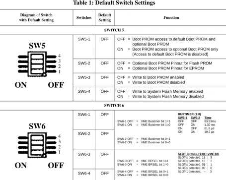
1.3 Default Switch Settings
The following table shows the default settings for all the switches on the board. Please make sure you check the default settings before powering up the board.
SEE ALSO: For the position of the switches on your CPU-30 R4 board,
[image:28.596.64.519.222.585.2]please see Figure 2, “Diagram of the CPU-30 R4 (Bottom View),” on page 4.
Table 1: Default Switch Settings
Diagram of Switch
with Default Setting Switches
Default
Setting Function
SWITCH 5
SW5-1 OFF OFF = Boot PROM access to default Boot PROM and optional Boot PROM
ON = Boot PROM access to optional Boot PROM only (Access to default Boot PROM is disabled)
SW5-2 OFF OFF = Optional Boot PROM Pinout for Flash PROM ON = Optional Boot PROM Pinout for EPROM
SW5-3 OFF OFF = Write to Boot PROM enabled ON = Write to Boot PROM disabled
SW5-4 OFF OFF = Write to System Flash Memory enabled ON = Write to System Flash Memory disabled
SWITCH 6
SW6-1 OFF BUSTIMER (1:0)
SW6-1 SW6-2 Time
SW6-1 OFF = VME Bustimer bit 1=1 OFF OFF 83.53ms SW6-1 ON = VME Bustimer bit 1=0 OFF ON 1.30 ms
ON OFF 81.6µs ON ON 10.2µs SW6-2 OFF = VME Bustimer bit 0=1
SW6-2 ON = VME Bustimer bit 0=0 SW6-2 OFF
SW6-3 OFF SLOT, BRSEL (1:0) : VME BR
SLOT-x detected, 11 : 3 SW6-3 OFF = VME BRSEL bit 1=1 SLOT-x detected, 10 : 2 SW6-3 ON = VME BRSEL bit 1=0 SLOT-x detected, 01 : 1 SLOT-x detected, 00 : 0 SW6-4 OFF = VME BRSEL bit 0=1 SLOT-1 detected, -- : 3 SW6-4 ON = VME BRSEL bit 0=0
SW6-4 OFF
☞
SW5
OFF
ON
1 2 3 4
SW6
OFF
ON
SWITCH 7
SW7-1 OFF OFF = RESET Switch enabled ON = RESET Switch disabled
SW7-2 OFF OFF = ABORT Switch enabled ON = ABORT Switch disabled
SW7-3 OFF OFF = SCSI active termination enabled ON = SCSI active termination disabled
SW7-4 OFF OFF = additional VME Bustimer enabled if VME slot-1 function detected (otherwise disabled) ON = VME Bustimer disabled
SWITCH 8
SW8-1 OFF OFF = VME slot-1 auto-detection enabled ON = VME slot-1 function disabled
SW8-2 OFF OFF = VME_SYSFAIL output enabled ON = VME_SYSFAIL output disabled
SW8-3 OFF OFF = VME_SYSRESET output enabled ON = VME_SYSRESET output disabled
SW8-4 OFF OFF = VME_SYSRESET input enabled ON = VME_SYSRESET input disabled
SWITCH 11
SW11-1 OFF OFF = Power backup from battery disabled ON = Power backup from battery enabled
SW11-2 OFF OFF = Power Backup from VME STBY disabled ON = Power Backup from VME STBY enabled
SW11-3 OFF OFF = NVRAM supplied by Power Backup disabled ON = NVRAM supplied by Power Backup enabled
SW11-4 OFF OFF = Default NVRAM access only ON = Optional and default NVRAM access
Table 1: Default Switch Settings (Continued)
Diagram of Switch
with Default Setting Switches
Default
Setting Function
SW7
OFF
ON
1 2 3 4
SW8
OFF
ON
1 2 3 4
SW11
OFF
ON
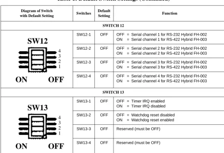
SWITCH 12
SW12-1 OFF OFF = Serial channel 1 for RS-232 Hybrid FH-002 ON = Serial channel 1 for RS-422 Hybrid FH-003
SW12-2 OFF OFF = Serial channel 2 for RS-232 Hybrid FH-002 ON = Serial channel 2 for RS-422 Hybrid FH-003
SW12-3 OFF OFF = Serial channel 3 for RS-232 Hybrid FH-002 ON = Serial channel 3 for RS-422 Hybrid FH-003
SW12-4 OFF OFF = Serial channel 4 for RS-232 Hybrid FH-002 ON = Serial channel 4 for RS-422 Hybrid FH-003
SWITCH 13
SW13-1 OFF OFF = Timer IRQ enabled ON = Timer IRQ disabled
SW13-2 OFF OFF = Watchdog reset disabled ON = Watchdog reset enabled
SW13-3 OFF Reserved (must be OFF)
[image:30.596.62.520.71.385.2]SW13-4 OFF Reserved (must be OFF)
Table 1: Default Switch Settings (Continued)
Diagram of Switch
with Default Setting Switches
Default
Setting Function
SW12
OFF
ON
1 2 3 4
SW13
OFF
ON
1.4 Front Panel
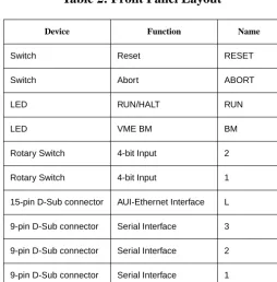
[image:31.596.192.446.177.435.2]The table below outlines the layout on the front panel. Additionally, there is a drawing of the front panel on the next page. The front panel devices are briefly described on the pages following the drawing.
Table 2: Front Panel Layout
Device Function Name
Switch Reset RESET
Switch Abort ABORT
LED RUN/HALT RUN
LED VME BM BM
Rotary Switch 4-bit Input 2
Rotary Switch 4-bit Input 1
15-pin D-Sub connector AUI-Ethernet Interface L
9-pin D-Sub connector Serial Interface 3
9-pin D-Sub connector Serial Interface 2
Figure 3: Front Panel
RESET
ABORT SYS68K/ CPU-30 R4
RUN BM
2
1
1 2 3 L
Rotary Switches
RESET and ABORT Keys
Status LEDs
15-pin D-Sub Connector
9-pin D-Sub Connector
9-pin D-Sub Connector
1.4.1 RESET and ABORT Keys
The RESET key generates an on-board reset. The ABORT key generates an IRQ on a programmable level. Both keys can be disabled via the switches described below:
1.4.2 Status LEDs The CPU-30 R4 includes two front panel LEDs: RUN/HALT LED and BM LED.
The RUN/HALT LED displays the condition that the processor is halted or reset is active and, in this case, the LED turns red. The RUN/HALT LED turns green on normal operation.
The bus master BM LED is used to indicate VMEbus mastership of the CPU-30 R4 and, in this case, the LED turns green.
1.4.3 Voltage Sensor The voltage sensor generates a power-up reset if the voltage level is below 4.75 V.
1.4.4 Watchdog Timer
This timer can be enabled by software and will generate an NMI followed by a power-up reset, when it is not retriggered.
1.4.5 Two Rotary Switches
Two software readable four-bit rotary switches are installed on the board and are accessible via the front panel.
SW7-1 Description
OFF (default) RESET key enabled
ON RESET key disabled
SW7-2 Description
OFF (default) ABORT key enabled
ON ABORT key disabled
SW13-2 Description
OFF (default) Watchdog reset disabled
1.5 Serial I/O Channels
The CPU-30 R4 has three serial I/O channels available via 9-pin D-Sub connectors on the front panel. All channels will support RS-232, RS-422 and RS-485 interfaces via the FORCE hybrids FH-00x. The default configuration is RS-232.
The following table shows the pinout of the serial I/O channels for RS-232.
NOTE: *With FH-002, this signal is provided by the hybrid being used.
The signal DTR is always driven active and the signal DSR is always read active by software. The RS-232 interface on your current CPU-30 revision 4.x board is fully compatible to the RS-232 interface on the earlier CPU-30 revision 3.2 board. However, the default jumper settings prescribed for the earlier board must be used to obtain this functionality.
1. Default terminal port setup: 9600 Baud, 8 data bits, 1 stop bit, no parity.
Table 3: 9-pin D-Sub Connector Pinout
1)(RS-232)
Pin Signal Direction Description
1 DCD in Data Channel Detector
2 RxD in Receive Data
3 TxD out Transmit Data
4 DTR out Data Terminal Ready
5 GND - Signal Ground
6 DSR in Data Set Ready
7 RTS out Request to Send
8 CTS in Clear to Send
9 GND* - Signal Ground
1
2
3
4
5 6
7
8
9
1.6 AUI-Ethernet
The AUI-Ethernet Interface is available on the front panel via a 15-pin D-Sub connector.
[image:35.596.191.381.178.406.2]The following table shows the pinout of the AUI-Ethernet connector.
Table 4: 15-pin AUI-Ethernet Connector
Pin Description
1 GND
2 Collision Detect+
3 Transmit Data+
4 GND
5 Receive Data+
6 GND
7 Not connected
8 GND
9 Collision
Detect-10 Transmit
Data-11 GND
12 Receive
Data-13 +12V
14 GND
15 Not connected
1
8
9
1.7 SCSI
The MB87033/34 provides an 8-bit single-ended SCSI interface. It is routed to the VMEbus P2 connector.
The termination is switch selectable and "TERMPWR" is supported. The following switches control the SCSI termination.
NOTE: TERMPWR is always supplied; if termination power is supplied
externally by a source other than the VME connector, the active termination is still maintained, although the VME may not be powered.
1.8 Parallel I/O (Option)
The parallel I/O signals are only available with the optional 5-row VMEbus P2 connector.
SW7-3 Description
OFF (default) SCSI active termination enabled
ON SCSI active termination disabled
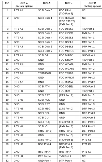
1.9 Connector Pinout for VMEbus P2
[image:37.596.188.514.123.641.2]NOTE: The signals marked in parenthesis are only available with the use
Table 5: Signal Assignment of the VME P2 Connector
PIN Row Z
(factory option)
Row A Row C Row D
(factory option)
1 PIT2 A0 SCSI Data 0 FDC RPM (TxD Port 2)
NC
2 GND SCSI Data 1 FDC HLOAD (FDC EJECT) (RxD Port 2)
NC
3 PIT2 A1 SCSI Data 2 FDC DSEL2 TxD Port 1
4 GND SCSI Data 3 FDC INDEX RxD Port 1
5 PIT2 A2 SCSI Data 4 FDC DSEL1 RTS Port 1
6 GND SCSI Data 5 FDC DSEL2 CTS Port 1
7 PIT2 A3 SCSI Data 6 FDC DSEL1 DTR Port 1
8 GND SCSI Data 7 FDC MOTOR DCD Port 1
9 PIT2 A4 SCSI DP FDC DIREC GND Port 1
10 GND GND FDC STEPX TxD Port 2
11 PIT2 A5 GND FDC WDATA RxD Port 2
12 GND GND FDC WGATE RTS Port 2
13 PIT2 A6 TERMPWR FDC TRK00 CTS Port 2
14 GND GND FDC WPROT DTR Port 2
15 PIT2 A7 GND FDC RDATA DCD Port 2
16 GND SCSI ATN FDC SDSEL GND Port 2
17 PIT2 H1 GND FDC RDY TxD Port 3
18 GND SCSI BSY (RTS Port 2) RxD Port 3
19 PIT2 H2 SCSI ACK GND RTS Port 3
20 GND SCSI RST GND CTS Port 3
21 PIT2 H3 SCSI MSG (CTS Port 2) DTR Port 3
22 GND SCSI SEL GND DCD Port 3
23 PIT2 H4 SCSI CD GND GND Port 3
24 GND SCSI REQ (TxD Port 3) DSR Port 1
25 PIT1 H1 SCSI IO (RxD Port 3) DSR Port 2
26 GND (RTS Port 1) (RTS Port 3) DSR Port 3
27 PIT1 H2 GND (CTS Port 3) PIT1 C0
28 GND (CTS Port 1) (TxD Port 1) PIT1 C1
29 PIT1 H3 DSR Port 4 DCD Port 4 (RxD Port 1)
PIT1 C4
30 GND RTS Port 4 RxD Port 4 PIT1 C7
31 PIT1 H4 CTS Port 4 TxD Port 4 NC
32 GND GND Port 4 DTR Port 4 NC
1.10 Introduction to VMEPROM Firmware
The VMEPROM firmware is a full multitasking multiuser real-time system. It is stored in the on-board System Flash Memory and provides the following functionality:
- Configuration of the board
- Starting an application
- Application hooks
- Shell with over 80 commands
- Programming of Boot Flash devices.
1.10.1 Booting up VMEPROM
To start VMEPROM, the rotary switches must both be set to ‘F’:
The different functions of the rotary switches are described in detail in the VMEPROM section of the SYS68K/CPU-30 R4 Technical Reference
Manual.
Correct Operation
To test the correct operation of the CPU board, the following command must be typed in:
The selftest command tests some I/O devices, the main memory and the system timer tick interrupt. Depending on the size of the main memory, it may last a different amount of time (count about one minute per megabyte).
After all tests are done, the following message will appear on the terminal screen:
Table 6: Rotary Switches
MODE 1 F
MODE 2 F
# SELFTEST <CR>
1.11 The SYS68K/IOBP-1
FORCE COMPUTERS offers an IOBP-1 back panel for easy connection of I/O signals through the VMEbus P2 connector. This board can be plugged into the VMEbus P2 connector of a VMEbus board which carries the SCSI, FDC, and serial I/O signals on the VMEbus P2. It contains a SCSIbus connector (P2), a floppy disk interface connector (P3), and a serial I/O connector (P5). All VMEbus P2 connector row A and C pins are routed to the 64-pin male connector (P4). The pinout of these connectors is shown in the following table.
Table 7: SYS68K/IOBP-1 Pin Assignment
PIN No. IOBP-1
P1
PIN No. VMEbus
P2
Row A Signal Mnemonic
Row B Signal Mnemonic
Row C Signal Mnemonic
32 1 DB 0 SCSI
-31 2 DB 1 SCSI GND
30 3 DB 2 SCSI - Drive Select 4 (2) FDC
29 4 DB 3 SCSI - Index FDC
28 5 DB 4 SCSI - Drive Select 1 FDC
27 6 DB 5 SCSI - Drive Select 2 FDC
26 7 DB 6 SCSI - Drive Select 3 (1) FDC
25 8 DB 7 SCSI - Motor On FDC
24 9 DB P SCSI - Direction In FDC
23 10 GND - Step FDC
22 11 GND - Write Data FDC
21 12 GND GND Write Gate FDC
20 13 TERMPWR SCSI - Track 000 FDC
19 14 GND - Write Protect FDC
18 15 GND - Read Data FDC
17 16 ATN SCSI - Side Select FDC
16 17 GND - FDC READY FDC
15 18 BSY SCSI
-14 19 ACK SCSI - GND
13 20 RST SCSI - GND
12 21 MSG SCSI
-11 22 SEL SCSI GND GND
10 23 C/D SCSI - GND
9 24 REQ SCSI
-8 25 I/O SCSI
-7 26
3 30 RTS SER - RXD SER
2 31 CTS SER GND TXD SER
1 32 GND SER - DTR SER
Table 7: SYS68K/IOBP-1 Pin Assignment (Continued)
PIN No. IOBP-1
P1
PIN No. VMEbus
P2
Row A Signal Mnemonic
Row B Signal Mnemonic
3 Hardware Description
This CPU board is a high performance single-board computer based on the 68030 microprocessor and the VMEbus. The CPU board also includes an enhanced Floating Point Coprocessor 68882. The board design utilizes all of the features of the powerful FORCE Gate Array FGA-002.
Besides the CPU-30 R4, there will be a CPU-30Lite R4 without a coprocessor, a SCSI, an Ethernet, and a floppy disk interface.
SEE ALSO: Please refer to Table 2, “Ordering Information,” on page 9
for more detailed information.
The CPU-30 R4 provides an A32/D32 VMEbus interface including DMA, up to 32-Mbyte shared DRAM on-board, up to 8-Mbyte System Flash, an Ethernet Interface, a single-ended SCSI interface, a Floppy interface, four RS-232 serial I/O channels, up to 256-Kbyte SRAM and a Real-Time Clock, both with on-board battery backup.
The shared DRAM is accessible from the 68030 CPU, the FGA-002 DMA controller, and also from other VMEbus masters.
The CPU-30 R4 has an Ethernet port as well as three serial ports available on the front panel permitting a console port, download and data communication channels.
One serial port, as well as the SCSI interface and the Floppy interface are available via the 3-row VMEbus P2 connector.
A 20-bit parallel interface and the three serial ports from the front panel are available via the optional 5-row VMEbus P2 connector.
The CPU-30 R4 is fully software compatible to the CPU-30 R3 with the exception of the floppy controller FDC37C65C, which has replaced the WD1772.
3.1 SYS68K/CPU-30 R4 Memory Map
Table 11: SYS68K/CPU-30 R4 Memory Map
Address range Device VMEbus accessible Cache Burst
Access width
0000.000016
…00xF.FFFF16
DRAM: contributing to shared RAM, address range depends on memory capacity
Y Y Y 32/16/8
00xx.000016
…F9FF.FFFF16
VME A32 extended address space (consecutive to DRAM)
n/a N N 32/16/8
FB00.000016
…FBFE.FFFF16
VME A24 standard address space n/a N N 32/16/8
FBFF.000016
…FBFF.FFFF16
VME A16 short address space n/a N N 32/16/8
FC00.000016
…FCFE.FFFF16
VME A24 standard address space n/a N N 16/8
FCFF.000016
…FCFF.FFFF16
VME A16 short address space n/a N N 16/8
FD00.000016
…FEEF.FFFF16
reserved n/a n/a n/a n/a
FEF0.000016
…FEF7.FFFF16
???
LAN - RAM N N N 32/16/8
FEF80.000016
…FEFF.FFFF16
???
LAN - Controller N N N 16
FF00.000016
…FF7F.FFFF16
The System PROM Area: address range depends on system flash ca-pacity
N N N 32/16/8 RO
32 WO
FF80.000016
FF80.0BFF16
reserved n/a n/a n/a n/a
FF80.0C0016
…FF80.0DFF16
PIT1 N N N 8
FF80.0E0016
…FF80.0FFF16
PIT2 N N N 8
FF80.100016
FF80.1FFF16
FF80.200016
…FF80.21FF16
DUSCC1 N N N 8
FF80.220016
…FF80.23FF16
DUSCC2 N N N 8
FF80.240016
…FF80.2FFF16
reserved n/a n/a n/a n/a
FF80.300016
…FF80.31FF16
Real-Time Clock – RTC 72423 N N N 8
FF80.320016
…FF80.33FF16
reserved n/a n/a n/a n/a
FF80.340016
…FF80.35FF16
SCSI-Controller N N N 8
FF80.360016
…FF80.37FF16
reserved n/a n/a n/a n/a
FF80.380016
…FF80.397F16
The Floppy Disk Controller N N N 8
FF80.397F16
…FF80.39FF16
Slot-1 status register (RO) N N N 8 ro
FFC0.000016
…FFCF.FFFF16
Local SRAM N Y N 32/16/8
FFD0.000016
…FFDF.FFFF16
FGA-002 Gate Array internal reg. n/a N N 32/16/8
FFE0.000016
…FFEF.FFFF16
Boot PROM N N N 32/16/8
FFF0.000016
…FFFF.FFFF16
reserved n/a n/a n/a n/a
Table 11: SYS68K/CPU-30 R4 Memory Map (Continued)
Address range Device VMEbus accessible Cache Burst
3.2 The CPU 68030 Processor
3.2.1 Hardware Interface of the 68030
The 68030 uses a nonmultiplexed address and data bus. Asynchronous signals allow easy interfacing to the outside world; synchronous signals perform fast interaction.
The CPU drives the address signals (A0-A31), the size signals (SIZ0, SIZ1) and the function code signals (FC0-FC2) on every cycle, independent of a cache hit or miss. These signals are used to decode the memory map of the CPU board.
The hardware on the CPU board is notified by the address and data strobe signals that the current cycle is not a cache cycle, and that the decoding outputs are strobed to be valid.
The 32 data lines (D0-D31) are also driven from the processor on write cycles and sensed on read cycles.
The size of the data transfer is defined by the SIZE + A0 - A1 output signals (always driven from the CPU). During asynchronous cycles the data bus width is determined by the Data Size Acknowledge Input signals (DSACK0, DSACK1). Synchronous cycles acknowledged by the Synchronous Termination Input signal (STERM) acknowledge the indicated data width during writes, whereas during reads a 4-byte width is always acknowledged.
If a bus error occurs (BERR sensed from the CPU), exception handling starts because the current cycle has been aborted (illegal transfer or incorrect data).
On local bus operation, a bus error will be generated if a device does not respond correctly.
VMEbus transfers may also be aborted via a BERR.
3.2.2 The
Instruction Set
3.2.3 Vector Table of the 68030
[image:45.596.135.516.97.680.2]This table lists all vectors defined and used by the 68030 CPU.
Table 12: Exception Vector Assignments
Vector Number(s) Vector Offset (Hex) Assignment
0 1
00016 00416
Reset Initial Interrupt Stack Pointer Reset Initial Program Counter
2 3
00816 00C16
Access Fault (Bus Error) Address Error 4 5 6 7 8 9 01016 01416 01816 01C16 02016 02416 Illegal Instruction Integer Divide by Zero CHK, CHK2 Instruction
FTRAPcc, TRAPcc, TRAPV Instructions Privilege Violation Trace 10 11 02816 02C16
Line 1010 Emulator (Unimplemented A-Line Opcode) Line 1111 Emulator (Unimplemented F-Line Opcode)
12 03016 Unassigned, Reserved
13 14 15 03416 03816 03C16
Coprocessor Protocol Violation Format Error
Uninitialized Interrupt
16-23 04016-05C16 Unassigned, Reserved
24 25 26 27 28 29 30 31 06016 06416 06816 06C16 07016 07416 07816 07C16 Spurious Interrupt
Level 1 Interrupt Autovector Level 2 Interrupt Autovector Level 3 Interrupt Autovector Level 4 Interrupt Autovector Level 5 Interrupt Autovector Level 6 Interrupt Autovector Level 7 Interrupt Autovector
32-47 08016-0BC16 TRAP #0-15 Instruction Vectors
48 49 50 51 52 53 54 55 0C016 0C416 0C816 OCC16 ODO16 OD416 0D816 ODC16
FPCP Branch or Set on Unordered Condition FPCP Inexact Result
FPCP Divide by Zero FPCP Underflow FPCP Operand Error FPCP Overflow FPCP Signalling NAN
FPCP Unimplemented Data Type
56 57 58 0E016 0E416 0E816
MMU Configuration Error
Defined for 68852, not used by 68030 Defined for 68852, not used by 68030
3.3 The Floating Point Coprocessor (FPCP)
The CPU board contains a Floating Point Coprocessor (FPCP 68882).
3.3.1 Features of the 68882
- 8 floating point data registers supporting 80-bit extended precision of real data (64-bit mantissa, 15-bit exponent, and one sign bit)
- Three registers for control, status and instruction address
- 67-bit arithmetic unit
- 67-bit barrel shifter
- 46 instructions with 35 arithmetic operations
- IEEE 754 compatible, including all requirements and suggestions
- Full set of trigonometric and transcendental functions
- Seven data types:
Byte Integer
Word Integer
Long Word Integer
Single Precision Real
Double Precision Real
Extended Precision Real
Packed Decimal Strings
- 22 constants available in the on-chip ROM, including Pi, e, and powers of 10
- Virtual memory/machine operations
3.3.2 Interfacing to the 68882
The 68882 is a non-DMA type coprocessor which uses a subset of the general purpose coprocessor interface supported by the 68030.
Features of the interface implemented in the 68882 are as follows:
- Main processor and 68882 communicate via standard bus cycles.
- Main processor and 68882 communication is not dependent upon instruction sets or internal details of individual devices (e.g. instruction pipes or caches, addressing modes).
- The main processor and 68882 may operate at different clock speeds.
- 68882 instructions utilize all addressing modes provided by the main processor; all effective addresses are calculated by the main processor at the request of the coprocessor.
- All data transfers are performed by the main processor at the request of the 68882; thus memory management, bus errors, address errors, and bus arbitration function as if the 68882 instructions are executed by the main processor.
- Overlapped (concurrent) instruction execution enhances throughput while maintaining the programmer's model of sequential instruction execution.
- Coprocessor detection of exceptions which require a trap to be taken are serviced by the main processor at the request of the 68882; thus exception processing functions as if the 68882 instructions were executed by the main processor.
- Support of virtual memory/virtual machine systems is provided via the FSAVE and FRESTORE instructions.
- Up to eight coprocessors may reside in a system simultaneously; multiple coprocessors of the same type are also allowed.
- Systems may use software emulation of the 68882 without reassembling or relinking user software.
3.3.3 Addressing the 68882
The 68882 is addressed via the function codes of the 68030 and a part of the address bus. This is done automatically within the opcodes generated by most 68030/68882 floating-point compilers and assemblers.
The following table lists the conditions for addressing the 68882.
3.3.4 FPCP ID Number
All instructions for the FPCP must include the coprocessor ID (001). Please note that the VMEPROM Assembler supports this function by default.
3.3.5 Detection of the 68882
The SENSE pin of the FPCP is connected to PI/T #1. This allows automatic detection whether or not the 68882 is installed.
CAUTION: PI/T #1 pin PC6/PIACK must be programmed as an input.
3.3.6 Summary of the 68882
Allowed Function Codes 1 1 1 (CPU Space Cycle)
Coprocessor ID 0 0 1
Usable Data Bits D0 - D31
Supported Transfer Types Byte
Word
Long Word
Signal Value Description
FC0 FC1 FC2
1 1 1
CPU Space Cycles
A13 A14 A15
1 0 0
Coprocessor ID = 1
A16 A17 A18 A19
0 1 0 0
Coprocessor Access Cycle
PC6 Function
0 FPCP installed
3.4 The Local Bus
3.4.1 The FGA-002 Gate Array
The CPU board also contains the FGA-002 Gate Array with 24,000 gates and 304 pins.
The FGA-002 Gate Array controls the local bus and builds the interface to the VMEbus. It also includes a DMA controller, complete interrupt management, a message broadcast interface (FMB), timer functions, and mailbox locations.
The gate array monitors the local bus. This in turn signifies that if any local device is to be accessed, the gate array takes charge of all control signals in addition to used address and data signals.
The FGA-002 Gate Array serves as a manager for the VMEbus. All VMEbus address and data lines are connected to the gate array through the buffers. Additional functions such as the VMEbus interrupt handler and arbiter are also installed on the FGA-002 Gate Array.
The start address of the FGA-002 Gate Array registers is FFD0.000016. All registers of the gate array and associated functions are described in detail in the FGA-002 Gate Array User’s Manual.
3.4.2 Shared DRAM The CPU board contains a Shared dynamic RAM area with a capacity of 4, 8, 16 or 32 Mbytes. The Shared RAM area is optimized for fast accesses from the 68030 CPU and the DMA controller in the FGA-002 Gate Array. The Shared RAM is also accessible by other VMEbus masters.
The Shared RAM area is arranged in 36-bit wide memory banks. There may be one or two of these banks on the CPU board, depending on the overall memory capacity delivered. Each 36-bit wide bank is separated into 32 data bits and 4 parity bits. A parity bit checks every eight consecutive data bits (byte parity). Advanced on-board memory control logic routes data to and from the on-board 68030 CPU, the DMA controller, and the VMEbus interface.
For every read cycle, regardless of size (byte, word, long-word or cache line) and regardless of master (68030, DMA or VMEbus), all 32 bits of data and 4 bits of parity are read from the Shared RAM array. The 32 data and 4 parity bits are stored in transceivers.
Write cycles are handled differently. In the case of a long-word access aligned to a 4-byte boundary, the DRAM can be written immediately. The parity info generated by FGA-002 will be written additionally to the DRAM. A synchronous termination signal (STERM) is asserted, and the cycle completed.
For all other write cycles (byte, word, long-word unaligned), the momentary valid parity info stored in DRAM must be read. Then the write to RAM Memory will be performed. Therefore, only the necessary data will be written, the remaining data already stored in DRAM will stay unmodified. Additionally, the new parity info generated by FGA-002 will be merged with the read parity info from DRAM and finally all four parity bits are written to DRAM. The synchronous termination signal (STERM) will be generated to complete the cycle.
All write cycles are terminated before they are fully processed to allow the master writing to DRAM to continue its operations (write posting).
3.4.2.1 Bank Selection of DRAM
The bank selection depends on memory size. The Dual-Banks architecture implements an interleaved organized DRAM (four consecutive bytes located in bank A, the next four consecutive bytes located in bank B, ...). The Single-Bank architecture implements a non-interleaved organized DRAM.
Shared RAM byte parity generation and check work for both local and VMEbus accesses. If a parity error is detected during a VMEbus slave read access, the CPU board drives BERR, informing the VMEbus master about the parity error. On all local accesses, a normal STERM will be generated, plus an interrupt on a software programmable level. The access address is stored inside the FGA-002 Gate Array allowing easy software controlled detection of the cycle which caused the parity error.
The Shared RAM is accessed from the VMEbus via FGA-002. The start and end access addresses are programmable in 4 Kbyte steps. The
1. FPM: Fast Page Mode
Table 13: Used Device Types for the Shared Memory
DRAM Device Device Capacity Total Capacity Bank Supported Product
1M * 4 FPM1) 9 * 1 Mbit * 4 4 Mbyte 1 CPU-30ZBE R4
1M * 4 FPM 18 * 1 Mbit * 4 8 Mbyte 2 CPU-30BE/8 R4
4M * 4 FPM 9 * 4 Mbit * 4 16 Mbyte 1 CPU-30BE/16 R4
4M * 4 FPM 18 * 4 Mbit * 4 32 Mbyte 2 factory option
1M * 4 FPM 9 * 1 Mbit * 4 4 Mbyte 1 CPU-30Lite/4 R4
defined memory range can be write protected in coordination with the VMEbus Address Modifier codes. For example, in privileged mode the memory could be read and written, while in non-privileged mode the memory could only be read, or a non-privileged access could be prohibited altogether.
When the gate array detects a VMEbus access cycle to the programmed address range of the Shared RAM, it requests local bus mastership from the CPU. After the CPU has granted local bus mastership to the FGA-002, the VMEbus access cycle is executed and all data is latched (read cycles), or stored to RAM (write cycles). The read and write cycle is then terminated and the FGA-002 immediately releases local bus mastership back to the CPU. Simultaneously, it completes the fully asynchronous VMEbus access cycle. The early completion of the memory read or write cycle allows the CPU to continue processing while the FGA-002 independently manages the VMEbus transaction overhead.
A programmable bit within the FGA-002 may be used to disable the early bus release option. With early release disabled, the FGA-002 retains local bus mastership until the VMEbus cycle is finished. This guarantees that no other local bus master (CPU or DMA controller) will access the Shared RAM until the VMEbus cycle is complete. In the case of a read-modify-write (RMW) cycle by another VMEbus master to the Shared RAM, the FGA-002 will perform both transactions (a read followed by a write) without releasing the local bus, thus guaranteeing that the cycle is indivisible.
In short, the early release option allows the CPU access to the Shared RAM sooner, but sacrifices the guaranteed indivisibility of VMEbus RMW cycles. Because the 68030 CPU includes an on-chip cache memory, this may not affect CPU performance at all.
3.4.3 Board Type with Memory Capacity
The following table lists the CPU board type with the memory capacity of the Shared RAM.
Board Type CPU Frequency DRAM Capacity
CPU-30ZBE R4 25 MHz 4 Mbytes
CPU-30BE/8 R4 25 MHz 8 Mbytes
CPU-30BE/16 R4 25 MHz 16 Mbytes
factory option 25 MHz 32 Mbytes
CPU-30Lite/4 R4 25 MHz 4 Mbytes
3.4.4 Reading the Shared RAM Capacity
The amount of Shared RAM may be read via three input pins from Port B of PI/T #2. The table below summarizes the encoding of these three bits.
SEE ALSO: Please refer to Section 3.10.13, ‘I/O Configuration of PI/T
#2,’ on page 74 for more detailed information.
3.4.5 Shared RAM
Addressing
The access address of the Shared RAM is programmable within the FGA-002 Gate Array. The default address range of the 4 Mbyte DRAM array is from 0000.000016 to 003F.FFFF16. The default address range of the 32 Mbyte DRAM array is 0000.000016 to 01FF.FFFF16. It is possible to program nearly any address range desired in the FGA-002.
The access address of the Shared RAM from the VMEbus is also programmable via FGA-002. That is the address range that other VMEbus masters must use in order to access the Shared RAM on the CPU board. This is not necessarily the same address range used by the CPU for local accesses.
SEE ALSO: Please refer to Section 3.18, ‘VMEbus Slave Interface,’ on
page 101 for more information.
3.4.6 Shared RAM
Performance
The memory interface logic controlling the Shared RAM array is optimized for fast accesses from the 68030 CPU, providing the highest possible performance. Because the 68030 CPU contains an on-chip data and instruction cache, many CPU accesses are cache line "burst fills". These burst transactions attempt to read 16 consecutive bytes into the 68030, using four 4-byte cycles.
B2 B1 B0 Memory Capacity
0 0 0 32 Mbytes
0 0 1 16 Mbytes
0 1 0 8 Mbytes
0 1 1 4 Mbytes
1 - - Reserved
Start Address End Address Memory Capacity
0000.000016 01FF.FFFF16 32 Mbytes
0000.000016 00FF.FFFF16 16 Mbytes
0000.000016 007F.FFFF16 8 Mbytes
0000.000016 003F.FFFF16 4 Mbytes
☞
The first read cycle of such a burst usually requires 5 CPU clock cycles (200 nanoseconds at 25 MHz). Due to the optimized design of the memory control logic, each subsequent cycle only requires 1 CPU clock cycle (40 nanoseconds) to complete. This is commonly called a "5-1-1-1" burst transfer. Overall, the total cache line "burst fill" operation requires 8 clock cycles to transfer 16 bytes, providing a memory bandwidth of over 50 Mbytes/second.
3.5 The System PROM Area
The first two read cycles after reset of the microprocessor are operand fetches of the Initial Interrupt Stack Pointer (ISP) and the Initial Program Counter (IPC). These operands are always fetched from addresses 0000.000016 and 0000.000416, respectively.
3.5.1 Initialization Special control logic in FGA-002 maps the Boot PROM (not the System Flash Memory) down to this address to allow the 68030 to boot from a single byte-wide PROM. This facilitates debugging and low-level program development. However, when the initialization routines in the Boot PROM are completed, control is transferred to the System Flash Memory in such a way that the 68030 appears to have been booted from the System Flash Memory, not the Boot PROM. For this reason, the System Flash Memory must also have the ISP and IPC loaded at address 0000.000016 and 0000.000416, respectively.
0000.000016 in System Flash Memory: Initial Interrupt Stack Pointer
0000.000416 in System Flash Memory: Initial Program Counter
3.5.2 Memory
Organization of the System PROM Area
The data path of the System Flash Memory is 32-bit wide, separated into 4-byte paths. Each byte path is connected to one Flash Memory device.
3.5.3 Read/Write to the System Flash Memory
Read cycles with any port size are allowed. Write cycles are flagged by the FGA-002 Gate Array with BERR. A programmable bit within the FGA-002 may be used to enable write operation to the System Flash Memory. In this case the FGA-002 will respond with an asynchronous data acknowledge (DSACK0, DSACK1). The write takes affect to the System Flash Memory depending on switch SW5-4.
The status of SW5-4 is connected to PI/T #2.
Pin PC4 on the PI/T #2 interface signal protects the write to the System Flash Memory and must be programmed as an input.
SW5-4 Description
OFF (default) Write to System Flash Memory enabled