LEAKAGE POWER REDUCTION IN WALLACE TREE
MULTIPLIER USING CURRENT COMAPRISON BASED
DOMINO LOGIC FULL ADDERS
1
R.NAVEEN, 2K.THANUSHKKODI, 3C.SARANYA
1Assistant professor, Department of ECE, IIE, Coimbatore 2Director, Department of EEE, ACET, Coimbatore
3Assistant professor, Department of ECE, IIE, Coimbatore
E-mail: [email protected], [email protected]
ABSTRACT
A lower power current comparison based domino logic 4*4 Wallace tree multiplier is proposed. Here the multiplier is designed by using low leakage high speed full adders. These full adders uses current comparison based domino logic to achieve low leakage and high speed. The technique which is utilized in this paper is based on comparison of mirrored current of the pull-up network with its worst leakage case current. This technique decreases the parasitic capacitance on the dynamic node, yielding a smaller keeper for wide fan-in gates to implement fast and robust circuits. So that the leakage current and power consumption and delay are reduced. The proposed 4*4 Wallace tree multiplier using current comparison based domino logic full adders was simulated using Mentor graphics ELDO in the temperature of 27o C, which is operated in 3 GHz shows half of the power reduction when compared to the 4*4 Wallace tree multiplier using standard full adders.
Keywords:Domino Logic, Wallace Multiplier, Power Dissipation, Full Adder, CMOS Logic
1. INTRODUCTION
The Multipliers play a major role in arithmetic operations in the digital signal processing application. Currently the need for low power multiplier has been increased due to the increasing demand for portable and mobile systems. C.S. Wallace suggested a fast multiplier [1] during 1964 with combination of half adders and full adders. The leakage power is high in this design. Later many researches were made on this multipliers. Among them the multiplier with full adders design had showed rapid development in reducing leakage power in 4*4 Wallace multipliers with full adders by domino logic.
There are three sources of power dissipation in CMOS technology 1) Dynamic power dissipation 2) Static power dissipation 3) Short circuit power dissipation. The dynamic power dissipation directly depends on the capacitance, voltage swing, leakage current on the switching node in the constant condition for frequency, power supply and temperature [2]. The static power dissipation depends on the leakage current that flows when the inputs and outputs of a gate
are not changing [2]. Short circuit dissipation depends on the short circuit current that flows directly from supply to ground when pull-up network and pull-down network of a CMOS gate conduct simultaneously [2].
In our work, we present a circuit level design method to reduce leakage power in conventional CMOS circuits. Here dynamic power dissipation is reduced in 4*4 Wallace tree multiplier using full adder by current comparison based domino logic. This paper is organized as follows 2) Existing method 3) Proposed method followed by results and conclusion in section 4 and 5.
2. EXISTING METHODS
In this section, we mainly survey the different techniques used to reduce leakage power in 4*4 Wallace tree multiplier. The 4*4 Wallace tree multiplier with full adder method replaces the full adders in the place of half adders. So there is no need for separate final summing unit as shown in figure 1. Hence the total leakage power is reduced [3].
The most of conventional methods concentrate on reducing static power and dynamic power
dissipation. The dynamic power is reduced by using different domino logic designs.
Figure 1: Multiplier using full adder
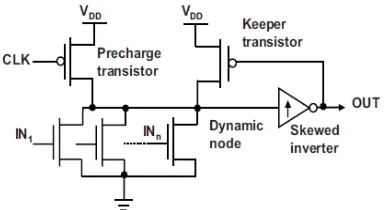
[image:2.612.104.301.135.340.2]The popular dynamic logic is standard domino circuit as shown in figure 2.
Figure 2: Standard Domino Logic
Here the multiplier is designed using standard domino logic style. In this design a PMOS keeper transistor is employed to prevent any undesired discharging at the dynamic node due to leakage currents and charge sharing of the pull-down networks (PDN) during the evaluation phase, hence improving the robustness[4]. However, the traditional keeper approach is less effective in new generation of CMOS technology. The keeper upsizing improves noise immunity, it increases leakage current between the keeper transistor and the evaluation networks. Thus, it increases power consumption and evaluation delay of standard domino circuits.
Another technique is conditional keeper domino logic style. This technique changes the
controlling circuit of the gate voltage of the keeper transistor as shown in figure 3. When this logic is used to design a multiplier the leakage power is comparatively large due to the change in the controlling circuit of the gate voltage of the keeper circuit [6].
Figure 3: Conditional Keeper Domino Logic
[image:2.612.99.291.402.507.2]When this logic design is used to design a multiplier the leakage current will be larger [5]. The similar technique which is used to reduce leakage power is high speed domino (HSD) as shown in figure 4.
Figure 4 : High speed Domino Logic
The static power dissipation is reduced by some of the popular techniques. The input vector method makes use of dependence of leakage current on the input vector to gate [7].Additional control logic is used to put the circuit in a low leakage standby state when it is idle and restored to its original state when reactivated. Thus to retain the original state information, it requires special latches thereby increasing the area of circuit by about five times in worst cases.
[image:2.612.349.531.416.501.2]is turned on while circuit is in active state and turned off when circuit is in idle state. This is done with the help of sleep signals. As leakage power varies exponentially with the threshold voltage, it is necessary for sleep transistor to have a high threshold voltage. This leads to use of multiple threshold voltage CMOS (MTCMOS) technology. This technique has emerged as a very popular technique for standby mode leakage power reduction. The use of this technique give rise to the existence of reverse conduction paths that reduce noise margin or as a worst case scenario results in complete failure of gates [9].The variation of MTCMOS technique is the dual threshold voltage technique (DTMOS) [10] which uses transistors with two different threshold voltages. The low threshold transistors are used for gates in the critical paths and high threshold transistor are used for gates which are not on critical path, which leads to larger leakage.
3. PROPOSED WORK
A 4*4 Wallace tree multiplier is designed using current comparison based domino logic full adders.4*4 Wallace multiplier has 12 full adders, where all these full adders are replaced by current comparison based domino logic full adders. By these adders dynamic power dissipation in the multiplier is reduced such that half of the total leakage power in the 4*4 Wallace tree multiplier is reduced. The concept of current comparison based domino logic is shown in figure 5.In this logic pull down network implements the logical function and it is separated from the keeper transistor by current comparison stage. This stage compares the pull up network current with the worst case leakage current. Here transistor Mk is added in series with the reference current to reduce power dissipation when the voltage of the output node has fallen to ground voltage. An important issue in this logic is the generation of reference voltage, which is the correct variation of the reference current according to the process variations to maintain the functionality of the proposed circuit. Generally process variations are due to random and systematic parameter fluctuations [11].
Figure 5: Concept Of Current Comparison Based Domino Logic
In this paper systematic variations are considered and it is assumed that in a given circuit design the threshold voltage of all NMOS transistors varies together with PMOS transistors.The systematic process variations in this proposed circuit is tracked by the replica keeper current method [12].
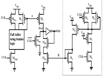
[image:3.612.323.536.372.529.2]Here the full adder is designed by current comparison based domino logic which uses the replica keeper current method to track the leakage current i.e., systematic process variation as shown in figure 6.
Figure 6: Implementation of full adder using current comparison based domino logic
voltage of transistors is only varied due to the process variation and not the body effect.
This proposed circuit can be divided to two stages. The first stage is pre-evaluation stage and second is domino stage. The first stage pre-evaluation network includes the pull up network and transistors MPre, MEval and M. The pull up network which implements the desired logic is disconnected from dynamic node Dyn, unlike traditional dynamic logic circuits, and indirectly changes the dynamic voltage. The second stage is domino stage has one input without any charge sharing, one transistor M2 regardless of the implemented full adder logic in the pull up network and a keeper which has two transistors. Hence only one pull up transistor is connected to the dynamic node instead of connecting all transistors in the full adder to reduce capacitance on the dynamic node.
The proposed circuit is operated in two modes, predischarge mode and evaluation mode. In predischarged mode, the input signals and clock voltage are in high and low levels respectively, [CLK = “0”, CLK = “1” in this phase. Therefore, the voltages of the dynamic node (Dyn) and node A have fallen to the low level by transistor MD is and raised to the high level by transistor Mpre, respectively. Hence, transistors Mpre, MDis, Mk1, and Mk2 are on and transistors M1, M2, and MEval are off. Also, the output voltage is raised to the high level by the output inverter.
In evaluation mode, clock voltage is in the high level [CLK = “1”, CLK = “0” and input signals can be in the low level. Hence, transistors
Mpre and MD is are off, transistor M1, M2, Mk2, and MEval are on, and transistor Mk1 can become on or off depending on input voltages. Thus, two states may occur. First, all of the input signals remain high. Second, at least one input falls to the low level. In the first state, a small amount of voltage is established across transistor M1 due to the leakage current. Although this leakage current is mirrored by transistor M2, the keeper transistors of the second stage (Mk1 and Mk2) compensate this mirrored leakage current. It is clear that upsizing the transistor M1 and increasing the mirror ratio (M) increase the speed due to higher mirrored current at the expense of noise-immunity degradation. In the second state, when at least one conduction path exists, the pull-up current flow is raised and the voltage of node A is decreased to nonzero voltage, which is equal to gate-source voltage of the saturated transistor M1. This voltage is also equal to
drain-source voltage of M1 and depends on size of M1 and its current. Increasing the pull-up current increases the mirrored current in transistor M2, thus voltage of the dynamic node Dyn is charged to VDD, yielding discharging the voltage of the output node and turning off the main keeper transistor Mk1. By this technique the contention current between the keeper transistor and the mirror transistor is mitigated. Here dynamic power dissipation is
reduced in the evaluation mode. This dynamic power dissipation is divided into two parts. First part is for the first stage of the proposed circuit and the second part is for the second stage. We know that the dynamic power dissipation directly depends upon the capacitance, voltage swing, leakage current on the switching node, frequency, power supply and temperature. Here power dissipation is reduced in both the stages. The first stages with n input has a lower voltage swing VDD to VTHP and has no leakage current due to less capacitance at dynamic node. The second stage has rail to rail voltage with minimum leakage. So by reducing voltage swing and capacitance, the dynamic power is reduced in both the stages with little area overhead. When a 4*4 Wallace tree multiplier is designed by using current comparison based domino logic full adder, the dynamic power dissipation is reduced such that total leakage power of the multiplier is reduced drastically.
4. RESULTS
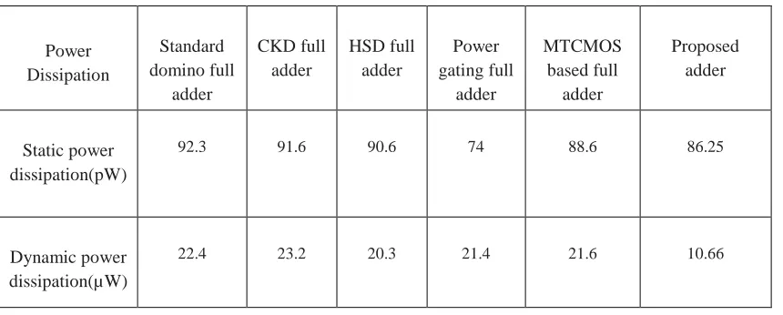
Table I: Simulation Result Of Current Comparison Based Full Adder
Table 2 : Simulation Result Of Multiplier
5. CONCLUSION
The leakage power of 4*4 Wallace tree multiplier is reduced by replacing half adders by full adders. But the leakage power is comparatively high during the operation mode of the multiplier. In order to reduce this leakage power, we present a current comparison based domino logic 4*4 Wallace tree multiplier. Here multiplier is designed by current comparison based domino logic full adders. By using this technique the parasitic capacitance on the dynamic node and voltage swing is reduced. So
the dynamic power dissipation is reduced to half of its magnitude when compared to the other techniques. Moreover, dynamic power dissipation contributes more to the total leakage power when compared to static and Short circuit power dissipation. From the simulation results, it can be concluded that the total leakage power has been drastically reduced by reducing half of the dynamic power dissipation.
Power Dissipation
Standard domino full
adder
CKD full adder
HSD full adder
Power gating full
adder
MTCMOS based full
adder
Proposed adder
Static power dissipation(pW)
92.3 91.6 90.6 74 88.6 86.25
Dynamic power dissipation(µW)
22.4 23.2 20.3 21.4 21.6 10.66
Power Dissipation
Standard domino full adder
based multiplier
CKD full adder based multiplier
HSD full adder based multiplier
Power gating full adder based
multiplier
MTCMOS based full adder based
multiplier
Proposed multiplier
Static power dissipation(pW)
98.3 96.5 94.2 82.3 89.2 86.25
Dynamic power dissipation(µW)
REFERENCES:
[1] C.S.Wallace, “A Suggestion for a fast multiplier”,IEE
Trans.Elechon.con@.,vol.EC-13,pp.14-17, Feb.1964
[2] Kaushik Roy, Sharat C. Prasad, “Low-power CMOS VLSI circuit design,”
Wiley-India, 2009
[3] D. Radhakrishnan, “Low-voltage low-power CMOS full adder,” IEEE Proc. Circuits Devices Syst., vol. 148, no. 1, pp. 19–24, Feb. 2004
[4] L.Wang, R. Krishnamurthy, K.
Soumyanath, and N. Shanbhag, “An
energy-efficient leakage-tolerant dynamic circuit
technique,” in Proc. Int. ASIC/SoC Conf.,
2000, pp. 221–225.
[5] A. Alvandpour, R. Krishnamurthy, K.
Sourrty, and S. Y. Borkar, “A sub-130-nm
conditional-keeper technique,” IEEE J.
Solid-State Circuits, vol. 37, no. 5, pp. 633–638, May 2002.
[6] M. H. Anis, M. W. Allam, and M. I.
Elmasry, “Energy-efficient noise-tolerant
dynamic styles for scaled-down CMOS and
MTCMOS technologies,” IEEE Trans. Very
Large Scale (VLSI) Syst., vol. 10, no. 2, pp. 71–78, Apr. 2002.
[7] Abdollahi, F. Fallah, and M. Pedram, “Leakage current reduction in CMOS VLSI circuits by input vector control,” IEEE
Transactions on Very Large Scale
Integration (VLSI) Systems, vol.12, no. 2,
pp. 140–154, February 2004.
[8] K. Agarwal, H. Deogun, D. Sylvester, and K. Nowka, “Power gating with multiple sleep modes,” Proceedings of the 7th International Symposium on Quality
Electronic Design, March 2006, pp. 633–
637.
[9] T. Douseki, S. Mutoh, Y. Matsuya, T. Aoki, S. Shigematsu and J. Yamada, “1-V power supply high-speed digital circuit technology with multithreshold-voltage CMOS,” IEEE Journal of Solid-State
Circuits, pp. 847-854, 1995.
[10] Q. Wang, and S. Vrudhula, “Static power optimization of deep submicron CMOS circuits for dual Vt technology,” Proceedings
of ICCAD, pp. 490–496, April 1998.
[11] K. Bowman, S. G. Duval, and J. D.
Meindl, “Impact of die-to-die and within-die parameter fluctuations on the maximum
clock frequency distribution for gigascale
integration,” IEEE J. Solid-State Circuits,
vol. 37, no. 2, pp. 183–190, Feb. 2002.
[12] Y. Lih, N. Tzartzanis, and W. W. Walker,
“A leakage current replica keeper for
dynamic circuits,” IEEE J. Solid-State