DLV11
-
E and 0 LV11-F
asynchronous
EK-DLV11-0P-001
DLV11-E and DLV11-F
asynchronous
Copyright © 1977 by Digital Equipment Corporation
The material in this manual is for informational purposes and is subject to change without notice.
Digital Equipment Corporation assumes no respon-sibility for any errors which may appear in this manual.
Printed in U.S.A.
This document was set on DIGITAL's DECset-8000 computerized typesetting system.
The following are trademarks of Digital EqUipment Corporation, Maynard, Massachusetts:
DEC DECCOMM DECsystem-lO DECSYSTEM-20
DECtape DECUS DIGITAL MASSBUS
PDP RSTS TYPESET-8 TYPESET-ll UNIBUS
CHAPTER 1
1.1
1.2
1.3
1.4 CHAPTER 22.1
2.2 2.3 2.3.1 2.3.2 2.3.3 2.3.4 2.3.5 2.3.6 2.3.7 2.3.8 2.3.9 2.3.10 2.3.11 2.3.12 2.3.13 CHAPTER 3 3.1 3.2 3.3 3.4 3.4.1 3.4.2 CHAPTER 4 4.1 4.2 4.3 4.4 4.4.1 4.4.2 4.4.3 4.4.4CONTENTS
INTRODUCTIONPURPOSE AND SCOPE . . . . . OPERATING FEATURES
MODULE SPECIFICATIONS . .
MAINTENANCE . . .
GENERAL DESCRIPTION GENERAL . . . . MODULE FUNCTIONS CIRCUIT FUNCTIONS
General Bus Interface I/O Control Logic Control/Status Registers Data Buffers . . . Receiver Active Circuit Interrupt Logic
Baud Rate Control Break Logic . . . . Maintenance Mode Logic DLVll-E Peripheral Interface DLVll-F Peripheral Interface DC-to-DC Power Inverter
INSTALLATION
GENERAL . . . . .
CONFIGURATION . . . . MODULE INSTALLATION
MODULE CHECKOUT . . . . DLVll-E Checkout . . . . DLVll-F Checkout . . . .
PROGRAMMING Page
1-1
1-1
1-3
1-3
2-1
2-1
2-3
2-3
2-3 2-4 2-4 2-7 2-7 2-7 2-8 2-8 2-8 2-8 2-9 2-93-1
3-1
3-1
· 3-11 · 3-15 · 3-15
INTRODUCTION . . . . 4-1 4-1 4-9 DEVICE REGISTERS . . . .
INTERRUPTS . . . . . . .
TIMING CONSIDERATIONS . . . . · 4-10
Receiver . . . . · 4-10
Transmitter . . . . · 4-10
BREAK Generation Logic . . . · 4-10
CHAPTERS 5.1 5.2 5.2.1 5.2.2 5.3 5.3.1 5.3.2 5.3.3 5.4 5.4.1 5.4.2 5.4.3 5.5 5.5.1 5.5.2 5.6 5.7 5.7.1 5.7.2 5.7.3 5.7.4 5.8 5.8.1 5.8.2 5.8.3 5.8.4 5.9 5.9.1 5.9.2 5.10 5.11 5.12 5.12.1 5.12.2 5.13
CONTENTS (CONT)
DETAILED TECHNICAL DESCRIPTION GENERAL . . . .
BUS INTERFACE . . . Address Decoding Vector Addressing I/O CONTROL LOGIC
Input Operation . Output Operation Vector Operation
CONTROL/STATUS REGISTERS CSR Data Flow
Input Operation . Output Operation DATA BUFFERS . . .
Receiver Operation Transmit Operation RECEIVER ACTIVE CIRCUIT INTERRUPT LOGIC . . .
DLVII-E Receiver Interrupts DLVII-F Receiver Interrupts Transmitter Interrupts Interrupt Transactions BAUD RATE CONTROL
Program Control Jumper Control External Control Clock Selection BREAK LOGIC . . .
Receive Operation Transmit Operation MAINTENANCE MODE LOGIC DLVII-E PERIPHERAL INTERFACE DLVII-F PERIPHERAL INTERFACE EIA Data Leads Only Operation Current Loop Operation . DC-TO-DC POWER INVERTER
APPENDIX A IC DESCRIPTIONS
A.l DC003 INTERRUPT LOGIC
A.4.2 A.5
CONTENTS (CONT)
Transmitter Operation . . . . 5016 DUAL BAUD RATE GENERATOR
APPENDIX B WIRE WRAP INSTRUCfIONS
B.l
B.2
B.3 B.4 Figure No. 2-1 2-22-3
3-13-2
3-3
3-4 3-54-1
4-2 4-34-4
4-5
4-6
4-7
5-15-2
5-3 5-45-5
5-6 5-7 5-8 5-9 5-10 5-115-12
PURPOSE . . . DEFINITIONS CONNECTIONS PROCEDURE .
FIGURES
Title
Interfacing Examples . . . . DLV11-E and DLV11-F Data Flow, Simplified Block Diagram DLV11-E and DLV11-F Functional Block Diagram
DLV11-E Jumper Locations DLV11-F Jumper Locations DLV11-E Cabling Example DLV11-F Cabling Examples Typical Backplane Configuration DLVI1-E RCSR Bit Assignments DLVl1-F RCSR Bit Assignments
DLV11-E and DLV11-F RBUF Bit Assignments DLV11-E and DLV11-F XCSR Bit Assigments DLV11-E and DLVl1-F XBUF Bit Assignments DLV11-F Programming Example
Serial Data Format . . . . DLV11-E and DLV11-F Addresses
DLV11-E and DLV11-F Interrupt Vectors I/O Control Logic, Block Diagram
Data Input Timing . . . . . Data Output Timing . . . . DLVl1-E RCSR Data Flow DLV11-F RCSR Data Flow
DLVll-E and DLV11-F XCSR Data Flow Control/Status Registers During DATI
Control/Status Registers During DATO or DATOB UART Signal Flow . . . .
DLV11-E and DLV11-F RBUF Data Flow
Page A-21 A-29 B-1 B-1
B-2
B-3 Page2-2
2-3
2-5
3-2
3-3
3-9 3-10 3-11 4-24-5
4-6
4-7
4-84-15
. 4-18
Figure No. 5-14 5-15 5-16 5-17 5-18 5-19 5-20 5-21 5-22 5-23 5-24 5-25 5-26 A-I A-2 A-3 A-4 A-5 A-6 A-7 A-8 A-9 A-lO A-ll A-12 A-13 A-14 B-1 B-2 B-3 B-4 B-5 B-6 Table No.
FIGURES (CONT)
Receiver Active Circuit Interrupt Vector Signal Flow Interrupt Timing . . . .
Title
Baud Rate Control Signal Flow Break Logic Receive Signal Flow Break Logic Transmit Signal Flow Maintenance Mode Logic
DLVII-E Peripheral Interface Signal Flow Data Lead Only Interface . . . . 20 rnA Transmitter and Reader Run Circuit Active Receive 20 rnA Current Loop Passive Receive 20 rnA Current Loop Interlock Jumper Data Flow
DC003 Simplified Logic Diagram
DC003 "A" Interrupt Section Timing Diagram
DC003 "A" and "B" Interrupt Section Timing Diagram DC004 Simplified Logic Diagram . . . . .
DC004 Timing Diagram . . . . DC004 Loading Configuration for Table A-2 DC005 Simplified Logic Diagram
DC005 Timing Diagram . . . . . DART Data Format . . . . DART Receiver - Block Diagram DART Transmitter - Block Diagram DART Pin Locations
5016 Block Diagram . . . . 5016 Pin Locations . . . .
Solderless Wrapped Connection on Wire Wrap Pin Full Turn . . . .
Half Turn
Two Levels of Wire Wrap Defective Wire Wraps
Loading the Wire Wrapping Kit
Table No. 3-3 3-4 3-5 3-6 3-7 3-8 4-1 4-2 4-3 4-4 4-5 4-6 4-7 5-1 5-2 5-3 A-I A-2 A-3 A-4 A-5 A-6 A-7
TABLES (CONT)
TitleData Bit Selections
Jumper Configuration When Shipped Module Application Examples . . . . DLVll-E 40-Pin Header Connector Pinning DLVll-F 40-Pin Header Connector Pinning DLVll-E and DLVll-F Edge Connector Pinning Register Addresses for Console Interfacing DLVll-E RCSR Bit Assignments . . . . DLVll-F RCSR Bit Assignments . . . . DLVll-E and DLVll-F RBUF Bit Assignments DLVll-E and DLVII-F XCSR Bit Assignments DLVll-E and DLVll-F XBUF Bit Assignments DLVll-E Programming Example
Register Selection . . . . Byte Selection (Output Operations Only) UART Clock Sources . . . . DC003 Pin/Signal Descriptions . . . . . DC004 Signal Timing vs Output Loading DC004 Pin/Signal Descriptions
DC005 Pin/Signal Descriptions UART Pin Functions
5016 Selectable Frequencies 5016 Pin Functions
1.1 PURPOSE AND SCOPE
CHAPTER 1
INTRODUCTION
The DLVII-E and DLVII-F are asynchronous line interface modules that interface the LSI-II bus to any of several standard types of serial communications lines. The modules receive serial data from peripheral devices, assemble it into parallel data, and transfer it to the LSI-ll bus. They accept data from the LSI-ll bus, convert it into serial data, and transmit it to the peripheral devices. The two modules differ in that the DLVll-E offers full modem control, whereas the DLVll-F supports either 20 rnA current loop or EIA-standard lines, but does not include modem control.
This manual describes these modules to the user. It treats the two modules together for those functions common to both, and separately for those areas in which they differ. It is assumed that the reader has a general familiarity with the operation of the LSI-II computer and with the requirements of the periph-eral equipment. Refer to Microcomputer Handbook, EB 06583 76, for detailed information about the LSI-ll.
1.2 OPERATING FEATURES
Each asynchronous line interface is constructed on a single 21.6 cm X 122.7 cm (8.5 in X 5.0 in) dual-height module. The module mounts in any slot in the LSI-II's backplane. Both the DL VI1-E and the DLVll-F have the following features:
• Jumper- or program-selectable crystal-controlled baud rates: 50, 75, 110, 134.5, 150,300,600, 1200, 1800,2000, 3600,4800, 7200, and 9600.
• Provisions for user-supplied external clock inputs for baud rate control.
• Jumper-selectable parity and data bit formats.
• LSI-ll bus interface and control logic for interrupt processing and vectored addressing of interrupt service routines.
• Control, status, and data buffer registers directly accessible via processor instructions.
• Program and peripheral connector plug compatible with the PDP-II DLII series of asynchro-nous line interface modules.
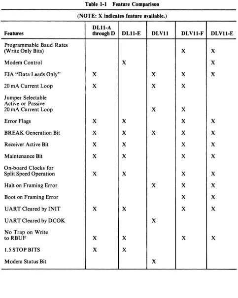
Table 1-1 Feature Comparison
(NOTE: X indicates feature available.) DLll-A
Features throughD DLll-E DLVll DLVll-F DLVll-E
Programmable Baud Rates
(Write Only Bits) X X
Modem Control X X
EIA "Data Leads Only" X X X X
20 rnA Current Loop X X X
Jumper Selectable Active or Passive
20 rnA Current Loop X X
Error Flags X X X X
BREAK Generation Bit X X X X X
Receiver Active Bit X X X X
Maintenance Bit X X X X
On-board Clocks for
Split Speed Operation X X X X
Halt on Framing Error X X X
Boot on Framing Error X X
UART Cleared by INIT X X X X
UART Cleared by DCOK X
No Trap on Write
to RBUF X X X X
1.5 STOP BITS X X
[image:10.617.61.545.114.721.2]1.3 MODULE SPECIFICATIONS
The following specifications and particulars are for informational purposes only and are subject to change without notice. .
Physical Characteristics Dimensions
Circuit Card
Length: 21.6 cm (S.5 in) Height: 12.7 cm (5.0 in) Width: 1.3 cm (0.5 in)
Cable Connection
Mounting Requirements
backplane.
Electrical Characteristics Module Type
DLVll-E: MS017 DLVll-F: MS02S
Power Requirements
1.0 A (nominal) @ +5 V ±5%, 5.0 W 150 rnA (nominal) @ +12 V ±5, I.S W
LSI-ll Bus Loading
Presents one bus load.
Environmental Characteristics Temperature
Operating Nonoperating
Humidity (Operating and Nonoperating) 10% to 95%, maximum wet bulb 32° C
(90° F) and minimum dew point 2° C (35° F)
Altitude Operating Nonoperating
1.4 MAINTENANCE
Circuit Card Plus Handles
22.S cm (S.9 in) 13.2 cm (5.2 in)
1.3 cm (0.5 in)
One 40-pin header connector
Plugs directly into any dual-height slots on the LSI-II backplane or LSI-II expansion box
5° C to 50° C (41 ° F to 122° F) -40° C to 66° C (-40° F to 151 ° F)
2.4 km (S,OOO ft) 9.1 km (30,000 ft)
num-Signal names in the DLV11-E and DLV11-F print sets are in the following basic form:
SOURCE SIGNAL NAME POLARITY
SOURCE indicates the drawing number of the print set where the signal originates. The drawing number of a print (K-3, K-4, K-5, etc.) is located above the title block.
SIGNAL NAME is the proper name of the signal. The names used in the print set are also used in this manual.
POLARITY is either H or L to indicate the voltage level of the signal: H ~ +3 V; L ~ ground.
As an example, the signal: (K-3) INIT H
originates on sheet K-3 of the drawings and means "when INIT is true, this signal is at approx-imately +3 V."
LSI-II bus signal lines do not carry a SOURCE indicator. These names represent a bidirectional wire-ORed bus. As a result, multiple sources for a particular bus signal exist. The LSI-II bus signal names begin with a "B" for "bussed."
The D LV 11-E module is shipped with an H3I5 modem test connector included. This is plugged into the interface cable in place of a data set when running maintenance programs. The DLVII-F does not use this test connector.
A paper tape diagnostic maintenance program is shipped with the module for checkout and mainte-nance. The following programs are available:
2.1 GENERAL
CHAPTER 2
GENERAL DESCRIPTION
The DLVll-E is designed to interface equipment that transmits and receives data over commu-nications lines and conforms to EIA Standard RS232C and CCITT Recommendation V.24. The DLVII-E is used by the program to control a communications data set through the use of control signals and handshake sequences.
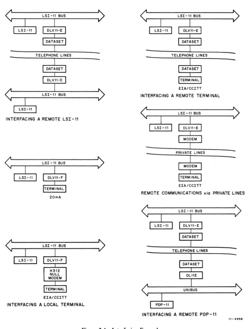
The DLVll-F supports either EIA-compatible data lines or 20 rnA current loop data lines. When configured for EIA support, the DLVll-F transmits and receives bipolar levels over the data lines to the device. This operation does not include control lines. When configured for 20 mA current loop operation, the DLVII-F can support either active or passive current loop devices. Figure 2-1 illustrates several applications of the modules.
2.2 MODULE FUNCTIONS
The DLVll-E and DLVll-F asynchronous line interface modules take data from the LSI-ll and convert it to the speed, character format, and signal levels required by the user's peripheral devices. Conversely, they assemble inputs from the peripheral devices into the format required for transfer to the computer. The computer program can address any of four registers in the interface modules to transfer data or status information. It can also enable the interface modules to generate interrupts. When a peripheral device requires service, the interface module will, if enabled, interrupt the program and vector to the necessary service routine.
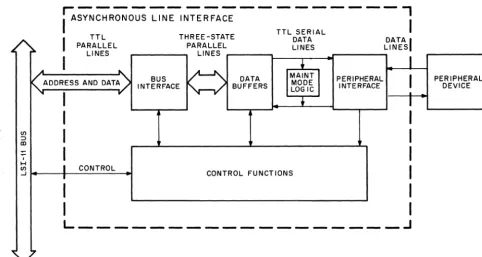
Data passes through three main circuits on its way to and from the peripheral device (Figure 2-2). During computer output operations, parallel data is taken off the LSI-II bus by a bus interface circuit and placed on the module's internal three-state bus. The data on the three-state bus enters a data buffer, where it is serialized and formatted for the peripheral device. From there it goes to a peripheral interface circuit that changes it from TTL to either EIA-compatible bipolar levels (DLVll-E or DLVII-F) or 20 rnA current loop signals (DLVII-F only). The data then leaves the module on an interface cable and goes to the user's peripheral device. Data coming into the computer from the peripheral device goes through this process in reverse order.
The control functions within the interface module are carried out by circuits that handle I/O transfers, interrupt requests, and control and status information. The DLVII-E interfaces control signals as well as data between the LSI-ll and the peripheral. The extent of this interaction is determined by the program and the type of perip.heral being supported.
LSI-II BUS
LSI-II BUS
INTERFACING A REMOTE LSI-II
20mA
LSI -II BUS
EIA/CCITT
INTERFACING A LOCAL TERMINAL
EIA/CCITT
INTERFACING A REMOTE TERMINAL
LSI-II BUS
EIA/CCITT
REMOTE COMMUNICATIONS via PRIVATE LINES
[image:14.617.61.561.67.723.2]I. ~ PARALLEL LINES PARALLEL LINES LINES LINESI
A
I
....C)
•
I
K
ADDRESS AND DATA) INTERFACE BUS BUFFERS DATA IMAINT I MODE PERIPHERAL INTERFACE I PERIPHERAL DEVICE... I
II'LOGIC
I
1
I
~~~~~~~~~~---l
I
TTL THREE-STATE TTLD~~:IAL DATAI
IUl
I
I
:::l In
I
I
I
H
I CONTROL
I
Ul
CONTROL FUNCTIONS
...J
I
I
I
I I
L _ _ _ _ _ _ _ _ _ _ _ _ _ _ _ _ _ _ ~
"Ii ~
[image:15.620.58.540.85.341.2]11-4959
Figure 2-2 DLVII-E and DLVII-F Data Flow, Simplified Block Diagram
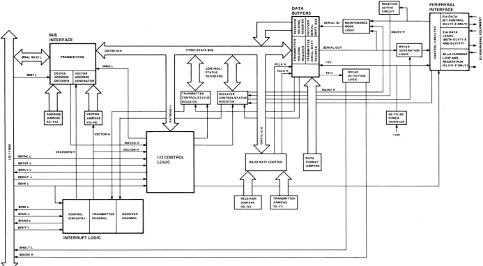
2.3 CIRCUIT FUNCTIONS
2.3.1 General
This section discusses the circuits on a functional level and is keyed to Figure 2-3. For a more detailed coverage of circuit operation, refer to Chapter 5.
2.3.2 Bus Interface
The bus interface circuit performs three basic functions:
1. It converts signal levels of data moving between the LSI-II bus and the interface module's internal three-state bus.
2. It decodes the device address and produces an address match (MATCH H) signal.
3. It generates interrupt vectors and places them on the LSI-ll bus.
The bus interface circuit monitors LSI-II bus lines BDALOO L through BDAL15 L. It inverts these signals and places them on three-state bus lines DATOO H through DAT15 H. If the information on the BDAL lines is the address of a location in the upper 4K of addressing space, i.e., in the I/O page, the LSI-II asserts BBS7 L. This signal enables the device address decoding function in the bus interface.
To decode the address, the circuit compares BDAL03 L through BDAL12 L with address jumpers A3 through A12. If the states of the BDAL lines match the corresponding jumpers the user has installed, the circuit sends MATCH H to the I/O control logic. MATCH H is a prerequisite for data transactions.
The bus interface logic generates vector addresses under the control of the interrupt logic and the vector address jumpers. The circuit creates two vectors; one for receiver interrupts and one for trans-mitter interrupts. The combination of VECTOR Hand VECRQSTB H from the interrupt logic and the states of vector address jumpers V3 through V8 determines what vector will be placed on the LSI-11 bus lines.
2.3.3 I/O Control Logic
The I/O control logic directs data transactions between the LSI-ll and the interface module. A data transaction can be a word or a byte, a high byte or a low byte, an input or an output, or status information or character information. The I/O control logic monitors the LSI-II bus lines to recog-nize what type of transaction is to be accomplished. It uses this information to control four device registers. The registers are named after their functions as follows:
Receiver Control/Status Register (RCSR)
Transmitter Control/Status Register (XCSR)
Receiver Buffer (RBUF)
Transmitter Buffer (XBUF)
These four registers are described in subsequent paragraphs of this chapter.
An I/O operation begins with the LSI-ll addressing the interface module. The bus interface decodes the address, asserts MATCH H to the I/O control logic, and places the address on the three-state bus lines. The I/O control logic decodes the three least significant bits of the three-state bus lines (DATOO H through DA T02 H) and the LSI-II bus control signals. The circuit develops register selection and byte selection signals to enable the correct data paths between the computer and the appropriate device register. It also controls INWD L, which determines whether the bus interface transceivers are trans-mitting or receiving. When data becomes available, the I/O control logic gates it to its destination (from the LSI-II bus to the three-state bus for an output transfer, or from the three-state bus to the LSI-II bus for an input transfer).
2.3.4 Control/Status Registers
The DLVII-E and DLVI1-F each have two control/status registers: the RCSR and the XCSR. The computer writes control bits out of these registers and reads status bits in from them. The registers consist of a series of latches, data selectors, and gating circuitry. During data transactions involving control and status information, the I/O control logic enables the XCSR or RCSR to either latch in control bits or gate out status bits.
N I Vl BUS INTERFACE TRANSCEIVERS
~)
. 1"~~~ __ ,-~~ __ -t~I~N~W~D~L---,
DEVICE
I
VECTOR BBS7 LBSYNC L
BWTST L
BRPLY l
BDOUT L
ADDRESS ADDRESS DECODER GENERATO.R
~
JUMPERSDRESS ~ECTOR
JUMPERS A3-A12 V3-VaVECTOR H
VECRQSTBH
'
-MATCHH VECTOR H
THREE·,nATE BUS
}=~.
I
:RANSM'TTER slI
r ,R=E::C=EI=V~ER:---S"'"\:=-1
CONTROllST ATUS CONTROLIST ATUS REGISTER /,;R:;;E::G~IS::T=;ER""' __ ~""'Ii---l
t :L
<7
-DATA BUFFERS
~ ~ E ~ ~ SERIAL IN I MAINTENANCE
I...--r---I ~ ~ ~ iii ~ 1+---11 MODE k-,
7
~ ~
%: :
~: sERIALouTa..;;;Lo;';G;;'lc~----'-ll RBUS:R~AK ~
- - , /- "\ z~
...
e_ i ~!!a ~ ~ GENERATION LOGIC :: ~::; ~ PERIPHERAL INTERFACE EIADATA LEADS tBOTH DLV11-E ANDDLV11·F)-
I----~-20mACURRENT ~ LOOP AND
-12V
~r---~----t-~~---;:;;;::::~----t--r~----t---~
TC~ FE H _I BREAK
I
READER RUN
tDLV11~ ONLY) ...
t,."T"-~--.,,~rJ----'-'=--4-1 ~~~;~TlON
MAINTH
I
OC-TO-OCI
POWER INVERTERf
+12V1/0 CONTROL
LOGIC
~
BAUD RATE CONTROL1
DATA FORMAT JUMPERSBDIN L
o
0
L
"'----.-:---11 1
1
1 - - - + - - - + - - - 1~--...I.----,-I---.&....-I'---. RECEIVER
I I
TRANSMITTERI
JUMPERS JUMPERS
BIROl BIAKI L BlAKe L alNIT L
BHALT L
BDCOK H
CONTROL TRANSMITTER RECEIVER CIRCUITRY CHANNEL CHANNEL
INTERRUPT LOGIC
[image:17.791.61.755.87.468.2]Not all control and status bits are both read and write; some are read-only bits and some are write-only bits. A detailed description of each bit is given with the programming information in Chapter 4.
2.3.S Data Buffers
The DLVII-E and the DLVII-F each have two data buffers: one for receive data (RBUF) and one for transmit data (XBUF). Both data buffers handle data by bytes. The RBUF also holds error flag bits pertaining to the status of the received data.
The data received from the peripheral device is transferred serially from the peripheral interface circuit into a receive shift register in the data buffer. From there it is transferred in parallel to a holding register. At the appropriate time, the buffer control circuitry places the parallel data, along with error information, onto the module's internal three-state bus. The bus interface then transfers the data to the computer.
Data to be transmitted to the peripheral device is taken off the three-state bus in parallel by the XBUF and then shifted serially out to the peripheral interface circuit.
Both the RBUF and the XBUF provide "double-buffering" of the data. The buffering is double in that the circuits each have both a serial shift register and a parallel holding register. This allows one charac-ter to be held while another is being moved into or out of the buffer.
2.3.6 Receiver Active Circuit
The receiver active circuit monitors the serial received data line from the peripheral interface and a receiver done (RDONE H) status bit from the RBUF. The circuit generates a busy signal (RBUSY H) to indicate that the receiver is active. This signal sets the RCVR ACT bit in the RCSR.
2.3.7 Interrupt Logic
When a peripheral device interfaced by a DLVll-E or DLVll-F needs service, the module can, if enabled, interrupt the computer program and vector to a service routine. The interrupt logic can initiate two types of interrupts: a receiver interrupt and a transmitter interrupt. These interrupts are handled through separate receiver and transmitter channels.
For an interrupt transaction to occur, first the program sets the interrupt enable bit in the con-trol/status register. Next, the interrupt logic recognizes the condition requiring service and asserts the interrupt request line (BIRQ L) to the computer. When the interrupt is acknowledged by the com-puter, the interrupt logic enables the bus interface to place the vector on the bus lines.
There are two vectors: one for a receiver interrupt and one for a transmitter interrupt. The interrupt logic uses VECRQSTB H to indicate which vector is enabled.
The LSI-II's interrupt acknowledge signal (BIAKI L/BIAKO L) is daisy-chained through the devices on the LSI-II bus. A device's priority is established by its position in the interrupt acknowledge daisy-chain. The interrupt acknowledge chain goes through both the receiver section and the transmitter section of the module's interrupt logic. It goes through the receiver section first, thereby giving the receiver channel priority over the transmitter channel.
A receiver interrupt is initiated when the RBUF has received and assembled a character of data and is ready to transfer it to the computer. A transmitter interrupt is initiated when the XBUF's holding register is empty and is ready for another data input from the computer.
2.3.8 Baud Rate Control
The baud rate control circuit generates clock signals that control the speeds at which the RBUF and XBUF move serial data. The circuit can provide a common clock to both data buffer circuits (common speed operation) or separate transmit and receive clocks (split speed operation).
In common speed operation, both transmit and receive baud rates are either set by wire wrap jumpers RO through R3 or programmable by three-state bus lines DAT12 H through DAT15 H. In split speed operation, the transmit baud rate is set by jumpers TO through T3, while the receive baud rate remains under the control of either RO through R3 or the computer program.
Should it be desired to use a baud rate not available from the baud rate control's crystal-controlled clock generator, the module has provisions for external inputs for both the transmit and receive clocks.
2.3.9 Break Logic
A BREAK signal is a continuous spacing condition on the serial data line. The DLVll-E and DLV11-F can receive BREAK signals from a peripheral device (normally the console device) and can transmit BREAK signals to a peripheral device (normally another processor). Either operation can be enabled or inhibited by wire wrap jumpers.
When the interface module receives a BREAK signal from the serial data line, it interprets the absence of STOP bits as a framing error. It can respond to this apparent error (or to an actual error) in one of three ways:
1. It can ignore it the apparent error.
2. It can place the LSI-ll in the HALT mode. 3. It can cause the LSI-II to re-boot.
Which action the module takes is controlled by wire wrap jumpers. To place the computer in the HALT mode, the break logic asserts BHALT L. To cause the computer to reload a bootstrap, the break logic negates BDCOK H. Refer to Paragraph 5.9 for further information.
2.3.10 Maintenance Mode Logic
The DLVII-E and DLVll-F have a maintenance mode for verifying the operation of the modules' data paths up to (but not including) the peripheral interface circuitry. This mode is controlled by the computer program, but is used only for checking the interface module, not the computer. In mainte-nance mode, data from the computer is transferred from the bus interface to the XBUF and serialized, as in normal operation. But then, in addition to going to the peripheral interface circuit, a sample of the XBUF's serial output is also routed back to the RBUF's serial input. There it is converted to parallel, placed on the three-state bus to the bus interface, and transferred back into the computer. The program can then compare the received data with the transmitted data to check for errors.
2.3.11 DLV11-E Peripheral Interface
The peripheral interface circuitry converts the DLVII-E's data and modem control signals from TTL levels to EIA-standard bipolar levels for the peripheral device. Likewise, it converts the peripheral's data and control lines from EIA levels to TTL levels for the interface module.
2.3.12 DLVll-F Peripheral Interface
The DLVII-F peripheral interface operates in one of two possible modes:
1. EIA Data Leads Only - This type of operation supports terminals that use EIA levels, but do not require control signal interaction.
2. 20 rnA Current Loop - This operation supports terminals that use either active or passive current loops. It also controls the paper tape reader on DIGITAL-modified TTY units that have a reader run relay.
When interfacing EIA-Ievel equipment, the module performs the TTL-to-EIA and EIA-to-TTL level conversion on the transmit and receive data leads only. During data leads only operation, the module does not monitor incoming control signals. Outgoing control signals (REQUEST TO SEND, FORCE BUSY, and DATA TERMINAL READY) are held by driver circuits in a continuous TRUE condition.
When the DLVII-F interfaces a 20 rnA current loop peripheral device, it can bejumpered to operate in either active or passive configuration. In the active configuration, the peripheral interface supplies the current for the loop; in the passive configuration, the current is supplied by the peripheral device. In either case, the receive data line from the peripheral is optically isolated from the DLVI1-F's internal data path.
The 20 rnA current loop transmitter operates in either the active or passive configuration. The transmit data lines are optically isolated from the DLVII-F's internal data path only in the passive configuration.
A Reader Run signal is produced for a peripheral device that has a reader run relay. When enabled by the program, the peripheral interface circuit supplies current to the relay, causing the reader to advance the paper tape.
2.3.13 DC-to-DC Power Inverter
3.1 GENERAL
CHAPTER 3
INSTALLATION
This chapter describes the jumper configuration, the installation requirements, and the checkout of the DLVll-E and DLVll-F asynchronous line interface modules. The wire wrap jumper functions are defined and application examples are presented. Wire wrapping instructions are presented in Appendix B.
3.2 CONFIGURATION
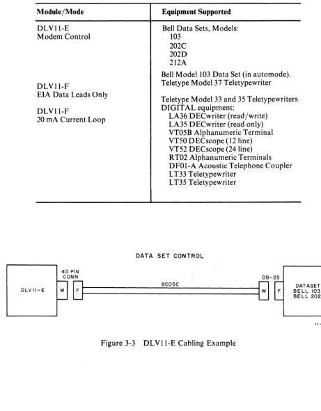
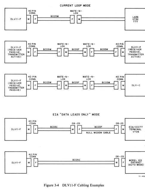
Before installing the module, ensure that it is configured for your application. The jumper locations are depicted in Figures 3-1 and 3-2. Their functions are defined in Tables 3-1, 3-2, and 3-3. Table 3-4 explains the configuration in which the modules are shipped from the factory. Table 3-5 lists common applications of the DLVll-E and DLV11-F; Figures 3-3 and 3-4 illustrate examples of typical cabling requirements.
The DLVll-F is shipped from the factory with capacitor C29 installed (Figure 3-2). This capacitor is provided for applications using Teletype® terminals. For applications using DIGITAL terminals, re-move capacitor C29.
3.3 MODULE INSTALLATION
The DLVll-E or DLVll-F module can be installed in any slots in the LSI-ll backplane, except the first four slots (the LSI-ll processor always occupies the first slots). Do not leave any unused option locations between the processor and the DLVll-E or DLV11-F. An open slot would break the inter-rupt acknowledge daisy chain. The priority of the module is determined by its proximity to the proces-sor on the bus (refer to Figure 3-5). The closer the slot is to the procesproces-sor module, the higher the interface module's priority.
Determine the appropriate slot for the module. For example, if a DLVll-E is interfacing commu-nications lines from a host computer, it would normally be placed in the slot closest to the processor module, followed by the module interfacing the console terminal. Refer to Microcomputer Handbook
S1
-Foll-FR
C1
-
M1ifni!
l~
'---___
---'
II
I" IIIII
y--B H
Figure 3-1 DLV11-E Jumper Locations
----
PB [image:22.618.56.545.77.695.2]["
~
liiiilili
II II
IIIII
Q
C29;a~ ilI~ M~!!:~
M"ItIIHC"",,CO
»»»
III111
Qp"NM
a: a: a: a:
IIII
Jumper
A3-AI2
V3-V8
RO-R3
TO-T3
BG
P
E
I, 2
PB
C,CI
S, SI
H
Table 3-1 Jumper Definitions
NOTE
This table pertains to both the DLVll-E and the DLVll-F, except as noted. Jumpers are inserted to enable the function they control except for those jumpers that indicate negation (such as "-B" and "B"). Negated jumpers are removed to enable the functions they control.
Function
These jumpers correspond to bits 3-12 of the address word. When inserted, they will cause the bus interface to check for a True condition on the corresponding address bit.
Used to generate the vector during an interrupt transaction. Each inserted jumper will assert the corresponding vector address bit on the LSI-II bus.
Receiver and transmitter baud rate select jumpers, during common speed operation.
Receiver only baud rate select jumpers during split speed operation (see Table 3-2).
Transmitter baud rate select jumpers during split speed operation.
Both receiver and transmitter baud rate if maintenance mode is entered during split speed operation (see Tale 3-2).
Jumper is inserted to enable Break generation.
Jumper is inserted for operation with parity.
Removed for even parity; inserted for odd parity. Receiver checks for appropriate parity and transmitter inserts appropriate parity.
These jumpers select the desired number of data bits (see Table 3-3).
Jumper is inserted to enable the programmable baud rate capability. These jumpers are inserted for common speed operation. (Note that S and Sl must be removed when C and Cl are inserted.)
Inserted for split speed operation. (Note that C and Cl must be re-moved when Sand SI are inserted.)
Jumper B, -B (DLVII-E)
B,lf
(DLVII-F)
-FD (DLVII-E only)
-FR (DLVII-E only) RS
(DLVII-E only) FB
(DLVII-E only)
IA,2A, and 3A (DLVII-F only)
IP, 2P (DLVII-F only)
4A,5A (DLVII-F only)
3P, 4P (DLVII-F only)
W
(DLVII-F only)
MT (DLVII-F only)
Table 3-1 Jumper Definitions (Cont) Function
Jumper B is inserted to negate BDCOK H when a BREAK signal or framing error is received, except when the Maintenance bit is set. This causes the LSI-II to reload the bootstrap. (Jumper -B orB must be removed when B is inserted.)
Jumper is removed to force DATA TERMINAL READY signal on.
Jumper is removed to force REQUEST TO SEND signal on.
This jumper is inserted to enable normal transmission of the REQUEST TO SEND signal.
Inserted to enable transmission of the FORCE BUSY signal (for Bell model 103E data sets).
These three jumpers are inserted to make the 20 rnA current loop receiver active. (Jumpers IP and 2P must be removed when lA, 2A, and 3A are inserted.)
These jumpers are inserted to make the 20 rnA current loop receiver passive. (Jumpers lA, 2A, and 3A must be removed when I P and 2P are install ed. )
Inserted to make the 20 rnA current loop transmitter active. (Jumpers 3P and 4P must be removed when 4A and 5A are inserted.)
Inserted to make the 20 rnA current loop transmitter passive. (Jumpers 4A and 5A must be removed when 3P and 4P are inserted.)
Jumper is removed to enable the error flags to be read in the high byte of the Receiver Buffer.
Table 3-2 Baud Rate Selections
Bit Bit Bit Bit Bit
Program Control 15 14 13 12 11*
Receive Jumpers R3 R2 Rl RO Baud
Transmit Jumpers T3 T2 Tl TO Rate
I I I I 50
I I I R 75
I I R I 110
I I R R 134.5
I R I I 150
I R I R 300
I R R I 600
I R R R 1200
R I I I 1800
R I I R 2000
R I R I 2400
R I R R 3600
R R I I 4800
R R I R 7200
R R R I 9600
I
=
Jumper Inserted=
Program Bit Cleared. R=
Jumper Removed=
Program Bit Set.*Bit 11 of the XCSR (Write Only Bit) must be set in order to select a new baud rate under program control. Also, jumper PB must be inserted to enable baud rate selection under program control.
Table 3-3 Data Bit Selections
Jumpers
2 1
I I
I R
R I
R
R
Number of Data Bits
5
6
Table 3-4 Jumper Configuration When Shipped
Jumper Jumper State
Designation DLVII-E DLVll-F Function Implemented
A3 R I Jumpers A3 through Al2 implement device address
A4 I R 1756lX for the DLVII-E and 17756X for the DLVII-F.
A5 I R The least significant octal digit is hardwired on the module
A6 I R to address the four device registers as follows:
A7 R I
A8 R R X=O RCSR
A9 R R X=2 RBUF
AIO I R X=4 XCSR
All R R X=6 XBUF
Al2 R R
V3 I I This jumper selection implements interrupt vector address
V4 I R 300s for receiver interrupts and 304s for transmitter
V5 I R interrupts on the DLVII-E. On the DLVll-F it selects
V6 R I 60s for receiver interrupts and 64 s for transmitter
V7 R I interrupts.
V8 I I
RO I I The module is configured to receive at 110 baud.
RI R R
R2 I I
R3 I I
TO I I The transmitter is configured for 9600 baud if split speed
T1 R R operation is used.
T2 R R
T3 R R
BG \ I I Break generation is enabled.
P R R Parity bit is disabled.
E R R Parity type is not applicable when P is removed.
1
R R Operation with 8 data bits per character.2 R R
Table 3-4 Jumper Configuration WhenShipped (Cont)
Jumper Jumper State
Designation DLVll-E ; DLVII-F Function Implemented
S R R Split speed operation disabled.
Sl R R
H R I Halt on framing error disabled on DLVII-E;enabled
on DLVll-F.
B R R Boot on framing error disabled.
-B I N/A
13
N/A I-FD I N/A The DATA TERMINAL READY signal is not forced
continuously True.
-FR I N/A The REQUEST TO SEND signal is not forced continuously
True.
RS I N/A The circuitry controlling the REQUEST TO SEND signal
is enabled.
FB R N/A The FORCE BUSY signal is disabled.
lA N/A I The 20 rnA current loop receiver is configured as an
2A N/A I active receiver.
3A N/A I
lP N/A R
2P N/A R
4A N/A I The 20 rnA current loop transmitter is configured for
5A N/A I active operation.
3P N/A R
4P N/A R
-
EF N/A I Error flags are enabled on DLVI1-E; disabled on DLVII-F.M R R Factory test jumpers. Not defined for field use.
Ml R R
Module/Mode
DLVII-E Modem Control
DLVII-F
Table 3-5 Module Application Examples
Equipment Supported
Bell Data Sets, Models: 103
202C 202D 212A
Bell Model 103 Data Set (in automode). Teletype Model 37 Teletypewriter EIA Data Leads Only
DLVII-F
Teletype Model 33 and 35 Teletypewriters DIGITAL equipment:
20 rnA Current Loop LA36 DECwriter (read/write)
LA35 DECwriter (read only)
OLV11-E
40 PIN
VT05B Alphanumeric Terminal VT50 DECscope (l2Iine) VT52 DECscope (24 line) RT02 Alphanumeric Terminals DFOI-A Acoustic Telephone Coupler LT33 Teletypewriter
LT35 Teletypewriter
DATA SET CONTROL
CONN OB-25
[image:29.618.66.528.94.686.2]~~
________________ B_CO_5_C __________________[j
Figure 3-3 DLVII-E Cabling Example
DATASET
BELL 103 BELL 202
DLVII -F
DLV"-F ( RECEIVER PASS IVE, TRANSMITTER
ACTIVEl
DLV11-F ( RECEIVER PASSIVE, TRANSMITTER
PASSIVEl
DLV11 -F
DLV"-F
CURRENT LOOP MODE
40 PIN
MATE-N-CONN. LOK
r:l
BC05Mr:l
LJI---1LJ
M L t - - - i40 PIN MATE-N- MATE-N- 40 PIN
CONN. LOK LOK CONN.
tJ
BC05M00
BC05FGtJ
BC05Mtl
40 PIN MATE-N- MATE-N- 40 PIN
CONN. LOK LOK CONN.
tJt--_B_C_0_5M _ _ 8 GI--_BC_0_5_F---IG 8 t - -_ _ B_C_0_5_M ____ t J
ErA" DATA LEADS ONLY" MODE
40 PIN
CONN DB-25 DB-25
[:]~
_ _ _ B_C_0_5C _ _ _~[:]
BC03P NULL MODEM CABLE40 PIN
CONN DB -25
[image:30.627.63.549.67.704.2][:]~ _ _ _ _ _ _ _ _ _ _ B_C_0_5_C _ _ _ _ _ _ _ _ _ _ _ [ : ]
Figure 3-4 DLVII-F Cabling Examples
LA36 VT52 TTY
DLV11-F ( RECEIVER PASSIVE, TRANSMITTER
ACTIVE)
DLII-C
EIA/CCITT TERMINAL
VT06
MODEL 103 DATASET (AUTO MODEl
CONNECTOR BLOCK
VI EW FROM MODULE SIDE OF BACKPLANE
A B C o
KDll-F
MSVl1 - B DLVl1- E MSVl1- B RXVl1 REVl1 DRVl1
Figure 3-5 Typical Backplane Configuration
2
3
4
11-4963
After the module has been configured properly and the desired location determined, install it in the computer as follows:
CAUTION
DC power must be removed from the backplane dur-ing module insertion and removal.
The module and backplane connector block may be damaged if the module is plugged in backwards.
1. Position the module so that the components side is facing row 1.
2. Slide the module into its slot, taking care that the module fingers mesh correctly with the backplane connector block.
3. Press the module into the connector block, making sure that the deep notch on the module seats against the connector block rib.
4. Next, plug the interface cable into the module's 40-pin header connector.
When the other end of the interface cable is installed, the module can be powered up and checked out. Interface cable installations are shown in Figures 3-3 and 3-4. Interface connector pinning is listed in Tables 3-6 and 3-7. Bus connector pinning is listed in Table 3-8.
3.4 MODULE CHECKOUT
Table 3-6 DLVll-E 40-Pin Header Connector Pinning Header
Berg M8017 Module BC05C Modem Cable
Pin Signal Names Signal Names
A Ground Ground
B Ground Ground
C Force Busy (EIA) Force Busy
D Sec. Clear to Send
E Serial Input (TTL) Interlock In
5
*
F Serial Output (EIA) Transmitted Data
H
J Serial Input (EIA) Received Data
K
L External Clock
M EIA Interlock Interlock Out
-N Serial Clock XMIT
P Sec Request to Send
R Serial Clock R CVR
S
T Clear to Send (EIA) Clear to Send
U
V Request to Send (EIA) Request to Send
W - Power
X Ring (EIA) Ring
Y + Power
Z Data Set Ready
AA
BB Carrier (EIA) Carrier
CC External Clock Input (TTL)
DD Data Terminal RDY (EIA) Data Terminal RDY
EE
FF Secondary XMIT (EIA) 202 Sec XMIT
HH
External Clock ENB (TTL)11 Secondary Rec (EIA) 202 Sec RCVR
KK
LL EIA SecXMIT
MM Signal Quality
NN EIA Sec RCVR
PP RR
SS Serial Output (TTL)
TT +5V
UU
Ground GroundVV Ground Ground
Table 3-7 DLVll-F 4O-Pin Header Connector Pinning
Header M8028 Module BCOSC Modem Cable
Pin Signal Names Signal Names BCOSM 20 mA Cable
A Ground Ground Ground
B Ground Ground
C Force Busy (EIA) Force Busy
D Sec Clear to Send
E Serial Input (TTL) Interlock In ~ --*- Interlock In ~
*
F Serial Output (EIA) Transmitted Data
H
20 rnA Interlock Interlock OutJ Serial Input (EIA) Received Data
K
Serial Input + (20 rnA) Received Data +L External Clock
M EIA Interlock Interlock Out
-N
Serial Clock XMITP Sec Request to Send
R Serial Clock RCVR
S Serial Input - (20 rnA) Received Data
-T Clear to Send
U
V Request to Send (EIA) Request to Send
W - Power
X
RingY + Power
Z Data Set Ready
AA Serial Output+(20 rnA) Transmitted Data +
BB Carrier
CC Ext. Clock Input (TTL)
DD Data Terminal RDY Data Terminal RDY
(EIA)
EE Reader Run - (20 rnA) Reader
Run-FF 202 SecXMIT
HH
Ext. Clock Enb (TTL)11 202 Sec RCVR
KK
Serial OutputLL EIASecXMIT
MM Signal Quality
NN
EIA Sec RCVRPP Reader Run+(20 rnA) Reader Run+
RR Signal Rate
SS Serial Output (TTL)
TT +5V
uu
Ground Ground GroundTable 3-8DLVll-E and DLVll-F Edge Connector Pinning
Mnemonic. Pin
~ ~ ", ;
+5 AA2
BA2
+12 AD2
BBS7L AP2
BDALOL AU2
BDAL1L AV2
BDAL2L BE2
BDAL3L BF2
BDAL4L BH2
,BDAL5 L BJ2
BDAL6L BK2
BDAL7L' BL2
BDAL8L BM2
BDAL9L BN2
BDAL lOL BP2
BDAL 11 L BR2
BDAL 12L BS2
BDAL13L BT2
BDAL14L BU2
BDAL 15 L BV2
BDINL AH2
BDOUTL AE2
BHALTL API
:' (,:" BIAK I L* AM2
BIAK 0 L* AN2
BINIT L AT2
BDMGIL* AR2
BDMGOL* AS2
BIRQL AL2
BRPLYL AF2
BSYNCL AJ2
BDCOKH BA1
GND AC2
GND( AT1
GND BC2
GND BTl
MSPARE A (-12 V) AK1~ **
ALI
MSPARE B (EXT R CLK) BK1'!J **
BL1
SSPARE4 BC1
SSPARE5 BD1
SSPARE6 BEl
SSPARE7 BF1
SSPARE 8 (EXT T CLK) BH1
3.4.1 DLVll-E Checkout
To verify the operation of the DLVII-E, turn off the dc power and remove the interface cable from the data set. Leave the other end connected to the module's header connector. Plug an H315 terminator into the free end of the interface cable. Power up the computer. Load and start MAINDEC-ll-DVDV A. When the program has been completed successfully, turn off the dc power and reconnect the interface cable to the data set.
3.4.2 DLVll-F Checkout
4.1 INTRODUCTION
CHAPTER 4
PROGRAMMING
Both the DLVII-E and DLVII-F are program compatible with PDP-ll software. Programs written for PDP-II's using DLlI-A through -D interface modules will run on an LSI-ll using a DLVll-F configured for the same application. Programs written for a DLlI-E will run with a DLVII-E. Also, the D L VII-F will operate with LSI-ll programs written for the DLVII.
This chapter defines the bits in each of the four device registers, discusses interrupts and timing consid-erations, and gives programming examples.
4.2 DEVICE REGISTERS
All software control of the DLVII-E or DLVII-F Asynchronous Line Interface is performed by means of four device registers. These registers have been assigned bus addresses and can be read or loaded (with the exceptions noted) using any LSI-II instruction referring to their addresses. Address assignments can be changed by altering jumpers on the module to correspond to any address within the range of 160000 to 177777. Table 4-1 lists the addresses of the registers when the module is used to interface a console device. The RCSR is at the base address. Each subsequent register is two locations up from the one preceding it.
Table 4-1 Register Addresses for Console Interfacing Register
Receiver Control/Status Register Receiver Buffer Register
Transmitter Control/Status Register Transmitter Buffer Register
Mnemonic RCSR RBUF XCSR XBUF
Address
177560 177562 177564 177566
Bit
15
14
13
12
II
[image:37.613.46.559.80.778.2], , - 4964
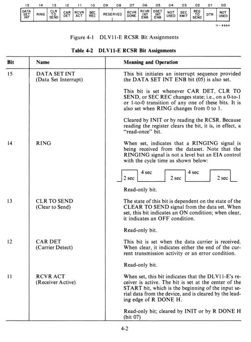
Figure 4-1 DLVII-E RCSR Bit Assignments
Table 4-2 DLVll-E RCSR Bit Assignments Name
DATA SETINT (Data Set Interrupt)
RING
CLRTOSEND (Clear to Send)
CARDET (Carrier Detect)
RCVRACT (Receiver Active)
Meaning and Operation
This bit initiates an interrupt sequence provided the DATA SET INT ENB bit (05) is also set.
This bit is set whenever CAR DET, CLR TO SEND, or SEC REC changes state; i.e., on a O-to-l or I-to-O transition of anyone of these bits. It is also set when RING changes from 0 to 1.
Cleared by INIT or by reading the RCSR. Because reading the register clears the bit, it is, in effect, a "read-once" bit.
When set, indicates that a RINGING signal is being received from the dataset. Note that the RINGING signal is not a level but an EIA control with the cycle time as shown below:
J
2 sec L . . I _4_se_c_---I1 2 sec 14 sec 2 secL
Read-only bit.
The state of this bit is dependent on the state of the CLEAR TO SEND signal from the data set. When set, this bit indicates an ON condition; when clear, it indicates an OFF condition.
Read-only bit.
This bit is set when the data carrier is received. When clear, it indicates either the end of the cur-rent transmission activity or an error condition. Read-only bit.
Bit
10
9-8
07
06
05
04
03
02
Table 4-2 DLVll-E RCSR Bit Assignments (Cont) Name
SECREC
(Secondary Received or Supervisory Received Data)
Not Used RCVRDONE (Receiver Done)
RCVRINTENB (Receiver Interrupt Enable)
DSETINTENB (Data Set Interrupt Enable)
Not Used SECXMIT
(Secondary Transmitted or Supervisory
Transmitted Data)
REQTOSEND (Request to Send)
Meaning and Operation
This bit provides a receive capability for the reverse channel of a remote station. A space (~+ 10. V) is read as a 1. (A transmit capability is provided by bit 03.)
Read-only bit.
Reserved for future use.
This bit is set when an entire character has been received and is ready for transfer to the LSI -Il. When set, initiates an interrupt sequence provided RCVR INT ENB (bit 06) is also set.
Cleared whenever the receiver buffer (RBUF) is addressed. Also cleared by INIT.
Read-only bit
When set, allows an interrupt sequence to start when RCVR DONE (bit 07) sets.
Read/write bit; cleared by INIT. See Note 1. When set, allows an inerrupt sequence to start when DATA SET INT (bit 15) sets.
Read/write bit; cleared by INIT. See Note 1.
Reserved for future use.
This bit provides a transmit capability for a reverse channel of a remote station. When set, transmits a space (~+ 10 V). (A receive capability is provided by bit 10.)
Read/write bit; cleared by INIT.
A control lead to the data set which is required for transmission. A jumper on the DLVII-E ties this bit to REQ TO SEND or FORCE BUSY in the data set.
Bit
01
Table 4-2 DLVll-E RCSR Bit Assignments (Cont)
Name Meaning and Operation
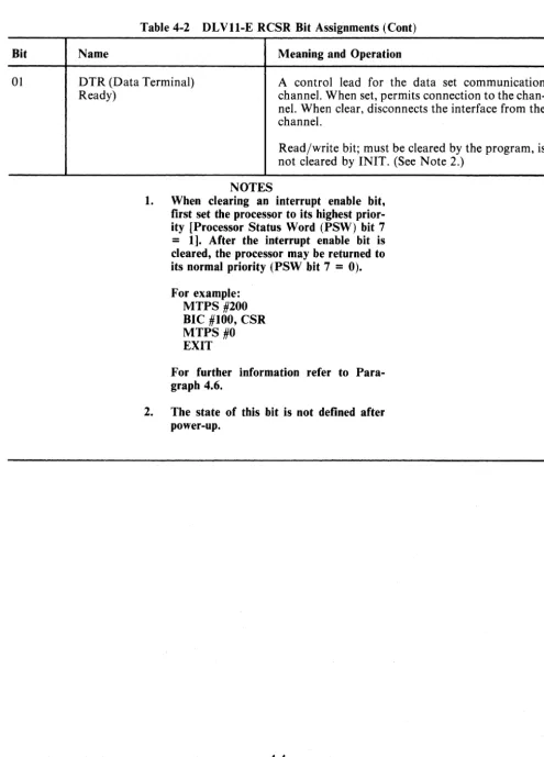
DTR (Data Terminal) Ready)
A control lead for the data set communication channel. When set, permits connection to the chan-nel. When clear, disconnects the interface from the channel.
Read/write bit; must be cleared by the program, is not cleared by INIT. (See Note 2.)
NOTES
1. When clearing an interrupt enable bit, first set the processor to its highest prior-ity [Processor Status Word (PSW) bit 7
=
1]. After the interrupt enable bit is cleared, the processor may be returned to its normal priority (pSW bit 7=
0).For example: MTPS #200 BIC #100, CSR MTPS #0 EXIT
For further information refer to Para-graph 4.6.
[image:39.623.59.554.66.755.2]Bit
15-12
11
10-08
07
06
05-01
00
,,- 4965
Figure 4-2 DLVII-F RCSR Bit Assignments
Name
Not Used
RCVRACT Receiver Active)
Not Used
RCVRDONE (Receiver Done)
RCVRINT ENB (Receiver Interrupt Enable)
Not Used
RDRENB (Reader Enable)
Table 4·3 DLVll·F RCSR Bit Assignments
Meaning and Operation
Reserved for future use.
When set, this bit indicates that the DLVII-F in-terface receiver is active. The bit is set at the center of the START bit, which is the beginning of the input serial data from the device, and is cleared by the leading edge of RDONE H.
Read-only bit; cleared by INIT or by RCVR DONE (bit 07).
Reserved for future use.
This bit is set when an entire character has been received and is ready for transfer to the LSI-II bus. When set, initiates an interrupt sequence provided RCVR INT ENB (bit 06) is also set.
Read-only bit; cleared whenever the receiver buffer (RBUF) is addressed or whenever RDR ENB (bit
00)
is set. Also cleared by IN IT .When set, allows an interrupt sequence to start when RCVR DONE (bit 07) sets.
Read/write bit; cleared by INIT.
Reserved for future use.
When set, this bit advances the paper-tape reader in DIGITAL-modified TTY units (LT33-C; LT35-A, -C) and clears the RCVR DONE bit (bit 07).
Bit
15
14
13
12
11-08
07-00
10 09 08 07 06 05 04 03 02 01 00
RESERVED RECEIVED DATA BITS
, , - 4966
Figure 4-3 DLVII-E and DLVll-F RBUF Bit Assignments
Table 4-4 DLVll-E and DLVll-F RBUF Bit Assignments Name
ERROR (Error)
OR ERR (Overrun Error)
FRERR (Framing Error)
PERR (Parity Error)
Not Used
Meaning and Operation
Used to indicate that an error condition is present. This bit is the logical OR of OR ERR, FR ERR, and P ERR (bits 14, 13, and 12, respectively). Whenever one of these bits is set, it causes ERROR to set. This bit is not connected to the interrupt logic.
Read-only bit; cleared by removing the error-pro-ducing condition.
NOTE
Error indications remain present until the next char-acter is received, at which time the error bits are updated. IN IT clears the error bits.
When set, indicates that reading of the previously received character was not completed (RCVR DONE not cleared) prior to receiving a new character.
Read-only bit. Cleared by INIT.
When set, indicates that the character that was read had no valid STOP bit.
Read-only bit. Cleared by INIT.
When set, indicates that the parity received does . not agree with the expected parity. This bit is
always 0 if no parity is selected.
Read-only bit. Cleared by INIT. Reserved for future use.
Bit
15-12
11
1~08
07
06
05':"03
02
10 09 08 07 06 05 04 03
RESERVED RESERVED
11-4967
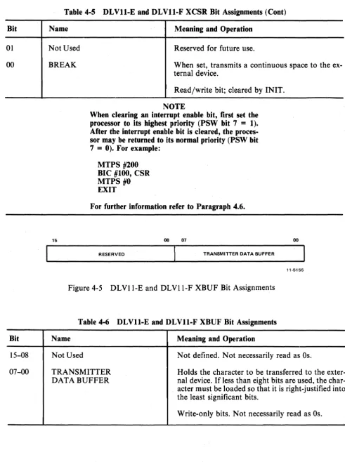
Figure 4-4 OLVII-E and OLVll-F XCSR Bit Assignments
Table 4-5 DLVll-E and DLVll-F XCSR Bit Assignments Name
PBR SEL (Programmable
Baud Rate Select) PBRENB (Programmable Baud Rate Enable) Not Used XMITROY (Transmitter Ready)
XMITINTENB (Transmitter Interrupt Enable) Not Used MAINT
Meaning and Operation
When set, these bits choose a baud rate from 50-9600 baud. See Table 3-2.
Write-only bits.
This bit must be set in order to select a new baud rate indicated by bits 12 to 15.
Write-only bits.
Reserved for future use.
This bit is set when the transmitter buffer (XBUF) can accept another character. When set, it initiates an interrupt sequence provided XMIT INT END (Bit 06) is also set.
Read-only bit; set by INIT.
When set, allows an interrupt sequence to start when XMIT ROY (bit 07) is set.
Read/write bits; cleared by INIT. See Note.
Reserved for future use.
Used for maintenance function. When set, con-nects the transmitter serial output to the receiver serial input while disconnecting the external device from the receiver serial input. It also forces the re-ceiver to run at transmitter baud rate speed when split speed operation is enabled.
Bit
01
00
Bit
15-08
07-00
Table 4-5 DLVll-E and DLVll-F XCSR Bit Assignments (Cont)
Name
Not Used
BREAK
15
Meaning and Operation
Reserved for future use.
When set, transmits a continuous space to the ex-ternal device.
Read/write bit; cleared by INIT.
NOTE
When clearing an interrupt enable bit, first set the processor to its highest priority (PSW bit 7
=
1). After the interrupt enable bit is cleared, the proces-sor may be returned to its normal priority (PSW bit 7=
0). For example:MTPS #200
BIC #100, CSR MTPS #0
EXIT
For further information refer to Paragraph 4.6.
08 07
RESERVED TRANSMITTER DATA BUFFER
00
11-5155
Figure4-5 DLVI1-E and DLVII-F XBUF Bit Assignments
Table 4-6 DLVll-E and DLVll-F XBUF Bit Assignments
Name
Not Used
TRANSMITTER DATA BUFFER
Meaning and Operation
Not defined. Not necessarily read as Os.
[image:43.615.56.548.73.732.2]The unused and load-only bits are always read as O's except for the XBUF, in which unused bits are undefined. Loading unused or read-only bits has no effect on the bit position. The mnemonic INIT refers to the initialization signal issued by the processor. Initialization is caused by one of the follow-ing: issuing a programmed RESET instruction; pressing "G" while in ODT; or the occurrence of a power-up or power-down condition of the processor power supply.
In the following descriptions, "transmitter" refers to those registers and bits involved in accepting a parallel character from the LSI-II for serial transmission to the external device; "receiver" refers to those registers and bits involved with receiving serial information from the external device for parallel transfer to the LSI-II.
4.3 INTERRUPTS
Both the DLVII-E and the DLVII-F have two interrupt channels: one for receiver interrupts and one for transmitter interrupts. These two channels operate independently. If, however, simultaneous inter-rupt requests occur, the receiver channel has priority over the transmitter channel.
In both the DLVI1-E and the DLVII-F, a transmitter interrupt can occur only if the interrupt enable bit (XMIT INT ENB) in the XCSR is set. With XMIT INT ENB set, setting the transmitter ready (XMIT RDY) bit initiates an interrupt request. When XMIT RDY is set, it indicates that the XBUF is empty and ready to accept another character from the bus for transfer to the external device. A receiver data interrupt can occur only if the interrupt enable (RCVR INT ENB) bit in the receiver RCSR is set. With RCVR INT ENB set, setting the receiver done (RCVR DONE) bit initiates an interrupt request. When RCVR DONE is set, it indicates that an entire character has been received and is ready for transfer to the bus. The receiver data interrupt occurs in both the DLVll-E and the DLVII-F. The DLVI1-E also has a data set interrupt.
The receiver portion of the DLVII-E handles multisource interrupts. One of the receiver interrupt circuits is activated by RCVR INT ENB and RCVR DONE. The other interrupt circuit can cause an interrupt only if the data set interrupt enable bit (DATA SET INT ENB) in the RCSR is set. With DATA SET INT ENB set, setting the DATA SET INT bit initiates an interrupt request. The DATA SET INT bit can be set by any of four other bits: CAR DET, CLR TO SEND, SEC REC, or RING.
NOTE
4.4 TIMING CONSIDERATIONS; , , '
When pro.gra~mingthe DLVII-E or,DLVll-F Asynchronous Line Interface, it is important to con-sider timing of certain functions in order to use the system in the most efficient manner. Timing considerations for the receiver, transmitter, and break generation logic are discussed in the following
par~graphs. "
4.4.1 Receiver
The RCVR ,DONE flag (bit 07 in the RCSR) sets when the receiver has assembled a full character. This occur~ at the middle of the first STOP bit.·Because the receiver is dOllble buffered, data remains valid until the next character is received and assembled. This permits one full character time for servicing the receiver interrupt..
4.4.2 Transmitter
The transmitter. is also double buffered. The XMIT RDY flag (bit 07 in the XCSR) is set after in-itialization. When the XBUF is loaded with the first character from the bus, the flag clears but then sets again within a function of a bit time. A second character can then be loaded, which clears the flag again. The flag then remains cleared for nearly one full character time. . ., . .
4.4.3 BREA~ Gener"ation Logic ,
When the BREAK bit (bit 00 in the XCSR) is set, it causes transmission of a continuous space. Because the XMIT RDY flag continues to function normally, the duration of a BREAK can be timed by the pseudo-tran~mission of a number of characters. However,because the transmitter is double buffered, a null character (all O's) should precede transmission of the BREAK to ensure that the previous character clears .the line. In a similar manner, the final pseudo-transmitted character in the BREAK should be null.
4.4.4 System Reset Timing
A system reset should not be performed immediately after the processor loads a character into the transmitter buffer for serial transmission. If the system is reset. before the last character has left the transmitter buffer, the character will be lost when the buffer is cleared by INIT. To avoid this, the program should transmit two m,lll characters after the last character, and then wait for XMIT RDY to
return to its true state. '
NOTE
Programs developed on the DLV-U Serial Line Unit (M7940) may not inclpde these null characters, since theDLV-Us transmitter buffer is nQt cleared by the
I~IT signal. '
4.5 PROGRAMMING EXAMPLES '
Table 4-7 is an example of a typical program that can be used as an echo program for a DLVll-E interfacing a Bell Model 103 data set. When a remote terminal dials in, this program answers the call and provides a character-by-character echo. Characters are also copied onto the console device.
Table 4-7 DLVll-E Programming Example
000200 .=200
000200 000167 001616 START· IMP BEGIN ;JUMP TO BEGINNING
;OFPROGRAM :SYMBOL DEFINITIONS
040000 RING= 040000 ;BIT 14 OF RCSR, RING
020000 crS= 020000 ;BIT 13 OF RCSR,
;CLEAR TO SEND
000200 RDONE= 000200 ;BIT 07 OF RCSR,
;RECEIVER DONE
000002 DTR= 000002 ;BIT 01 OF RCSR, DATA
;TERMINAL READY
000200 XRDY= 000200 ;BIT 07 OF XCSR,
;TRANSMITTER READY
002000 .=2000
002000 175610 RCSR: 175610 ;CSR OF RECEIVER
002002 175612 RBUF: 175612 ;BUF OF RECEIVER
002004 175614 XCSR: 175614 ;CSR OF TRANSMITTER
002006 175616 XBUF: 175616 ;BUF OF TRANSMITTER
002010 177564 CXCSR: 177564 ;CSR OF CONSOLE
;TRANSMITTER
002012 177566 CXBUF: 177566 ;BUF OF CONSOLE
;TRANSMITTER
002014 000000 BUFFER: 0 ;HOLDS CHARACTER
;RECEIVED
002016 000000 DELAY: 0 ;HOLDS DELAY COUNT,
;HIGHORDER
002020 000000 0 ;HOLDS DELAY COUNT,
;LOWORDER ;BEGINNING OF ECHO PROGRAM
002022 005077 177752 BEGIN: CLR @RCSR ;ST ART BY INITIALIZING
;ALL BITS TO ZERO
002026 032777 040000 177744 LOOPl: BIT # RING ,@RCSR ;CHECK FOR INCOMING CALL
002034 001774 BEQ LOOP 1 ;BRANCH IF PHONE IS NOT
;RINGING
002036 052777 000002 177734 BIS #DTR,@RCSR ;PHONE IS RINGING, SO
;ANSWER WITH DTR
[image:46.613.61.576.118.631.2]Table 4-7 DLVll-E Programming Example (Cont)
002052 032777 020000 177720 LOOP2: BIT #CTS,@RCSR ;CHECK FOR CLEAR
;TO SEND
002060 001007 BNE LOOP3 ;BRANCH IF ON
002062 162767 000001 177730 SUB #1,DELAY+2 ;CHECK DELAY
002070 005667 177722 SBC DELAY ;DECREMENT A
;TWO-WORD INTEGER
002074 001752 BEQ BEGIN ;BRANCH IF WE HAVE
;WAITED TOO LONG
002076 000765 BR LOOP2 ;BRANCH AND CONTINUE
;TO WAIT FOR CTS
002100 032777 020000 177672 LOOP3: BIT #CTS,@RCSR ;IS CHANNEL STILL
;ESTABLISHED?
002106 001745 BEQ BEGIN ;BRANCH IF CTS NOT
;PRESENT
002110 032777 000200 177662 BIT #RDONE,@RCSR ;CHECK FOR RECEIVED
;CHARACTER
002116 001770 BEQ LOOP3 ;BRANCH IF NO
;CHARACTER RECEIVED
002120 017767 177656 177666 MOV @RBUF,BUFFER ;READ RECEIVED
;CHARACTER INTO BUFFER
002126 032777 000200 177650 LOOP4: BIT #XRDY,@XCSR ;CHECK FOR TRANSMITTER
;READY
002134 001774 BEQ LOOP4 ;BRANCH IF NOT READY
002136 016777 177652 177642 MOV BUFFER,@XBUF ;TRANSMIT CHARACTER
;TO REMOTE TERMINAL
002144 032777 000200 177636 LOOPS: BIT #XRDY,@CXCSR ;CHECK FOR CONSOLE
;TRANSMITTER READY
002152 001774 BEQ LOOPS ;BRANCH IF NOT READY
002154 016777 177634 177630 MOV BUFFER,@CXBUF ;TRANSMIT CHARACTER
;TOCONSOLE
002162 000746 BR LOOP3 ;BRANCH AND WAIT FOR
[image:47.613.57.579.119.520.2]