Chapter 3 (cont)
4
5
CONTENTS
(continued)
I/O Skip Control and I/O' Trap
...
3-31'
Break, Contro I (32) ••••••••••••••• ~ ... ~ ~ ••••
3 ... 33
Interface •••••• " ... -... , ... .3-36
'Device Selector (36) ... e . . . e'. e • • • •3-37
Inf~rmation Collector (33) ... " " ••••••••••
3-39
Information Distributor
(34) ...
e ~ •3-40
MB Bus Drivers (28)...
3-40
CORE MEMORY ••••••••••••• , •••••••••••••••• " •••••••••• ~ ••••
4-1
Me~ory Organization .. " e._ .. " " . . . e .... " • • • " • " • • • • • • " " " • " •
4-1
Circui't Operations e . . . " . . . ~ ..Ferrite-Core Memory Array •••••••• : ... ' •.••••••••• Memory Selectors Type G202 and Memory Selector
Matrixes Types G60l and G602 ... :." ,,'. Inhibit Dri'/ers Type G201 ... " ... . Sense Amplifiers Type GOal and Master Slice
Con tro I Type G002 • e" . . . " . . . " . . ..
Memory Contro I
...
"...
'.'Memory Curren t Sources
...
INPUT/OUTPUT • • • • • • , ' . ~.' . . . ' • • • • • • • • • It • • • • • • • • • • • • • • • •Teletype (Model 33KSR) and Control Type 649 ... " ... . Block Diagram Discussion
...
Logical Functions ... " ... , ... ~ ... " ... .. Circuit Operations...
Perforated Tope Reader and Control Type 444B...
LogIcal Functions ... " .. Circuit Operations ... " ... "." ... ,,' ••• . . ' Tope Punch and Punch Control Type 75D...
~Logical Functions ... II • • " . . . .
Circuit Operations . . . of •
vii
4-2
4-2
4-4.4-8
4-8 4-104-11
5-15-3
5-3
5-5
5-6
5-8
5~ 11
5-15
7
CONTENTS (continued)
OPTIONAL EQUIPMENT • • • • • • • • • • • • • • • • • • e· • • • • • • • • • • • • • • • • • • • • Automntic Priority Interrupt Type
172 •••••••••••••••••••••••••
Block Diagram 0 iscussion .... oOoO . . . oO • • • • oO . . . oO.
Logical Functions ... .
Circuit Operations
...
Data Interrupt Multiplexer Type 173
...
Logical Functions ... ..Circuit Operations ... ., ... .
Extended Arithmetic Element Type
177 ..
oOoO . . . oOoOoOoOoOoO.oOoOoOoO .. oOoO .. oO .. oO.Logical Functions ... .
Circuit Operations
INTERFACE • • ,. • • • • 9 • • • • • • • • • • • • • • • • • • • • • • • • • • • • • • • • • • • • • • • • • •
Interface Conn€..:tions and Signal Identification
Loading and Driving Considerations ... oO .. oOoO .. oOoOoO . . . oO. oO" .. oOoO . . . Information Collector (lC) (33) .oO . . . oO • • oO.oOoO.oO • • oO • • oO.oO.oO • • oO . . . oO .. oO
Information Distributor (10) (34) oO . . . oOoOoOoO • • oOoO.oO • • • oO . . . oO .. oO ..
Device Selector (DS) (36)
...
PWR CLR and NE G. PWR CLR (20) ... If "oO . . . .. S'G f'J (B) (20) ... oOoO . . . oO . . . oO .. oOoOoOoOoO . . . . oOoOoO . . . . oO .. oOoO •• oOoOoOoO.oO . . . oO .. oOoOoO RUN STOP (20)
RUN ('1) (23)
...
MB
(36)...
10 T (36) •••••••••••••••••••••••••••••••••••••••••••••••••• ACB (34)
...
REQUEST SLOvV CYCLE (36)
...
PR0GRAM INTERRUPT REQ UEST (32) ... oOoOoO.oO . . . oO.oO • • oO • • • oO . . . oO DATA RQ (24) •••••••••••••••••• ' •••••••••••••••••••••••••••
. riA
(Data Address) (29)...
CONTENTS
(continu
ed)"
Chapter Page
7 (cant)
8
9
DATA ADDR ACC (32) • • • • • • • • • • • • • • • • • • • • • • • • • • • • • • • • • • • 41 •
DATA I N (Transfer 0 irectian) (32)
...
,..
-...
o
I {Data Information} (30)...
DATA ACC (32)MBB
(28
and 36)DATA ROY (32)
· ...
.,... .
• • • • • • • • • • • • • • • • • • • • • • • • • • • • • • • • • • • • • • • • f) •
• • • • • • • • • • • • • • • • • • • • • • • • • • • • • • • • • • • • • • • • • t) •
INSTALLATION
· ... .
Site Preparation " ••••••••••••••••••••••••••••••••••••••••• ".
Space Considerations
Environmental Conditions ••••••••••••••••••••••••••••• I I .
Power Requirements . . . .
Preparation for Sh ipment
Teletype Shipping Procedure ••••••••••••••••••••••
Installation •••••••••••••••• • • • • • • • • • • • • • • • • • • • • • • • • • • • • • G •
• • • • • • • • • • • • • • • • • • • • • • • • • • • • . • • • • • • • • • • • • • • • • • • • 4t •
Controls and Indicators ••••••••••••••••••••••••••••••••
Operator Console Controls and Indicators ••••••••••••
Teletype Controls
Tape Reader Controls
...
...
'..
Indicator Panel • • • It • • • • • • • • • • • • • • • • • • • • • • • • • • • • • • • • •
Operating Procedures
·
... .
Manual Data Storage and Modification
...
Loading Binary Data Using READ-IN Key ... .
Loading Data Under Program Control ... .
Assembl ing Program With PAL •••••••••••••••••••••••••••
Teletype Code
...
Local Teletype Operation
...
;.... .
Programming...
Chapter 10
11
CONTENTS
( con
tJ
n u e
d )
MAINTENANCE
...
Preventive Maintenance Mechanical Checks Power Supply Checks
...
...
...
·
... .
Marginal Checks Memory Current Check Sense Amplifier Check
...
...
Corrective Ma intenance
...
• • • • • • • • • • • • • • • • • • tJ • • • • • • • • • • • •
Prel iminary Investigation System Troubleshooting Circuit Troubleshooting
•••••••••••••••••••• i' ••••••••••••
...
...
Repair
Spare Ports
·
... .
V:Jiidaticn,Test ••••••••••••••••••••••••••••••••••••••••Log Entry •••••••••••••••.•••••••••••••••.••••• e . • • • • • • •
ENGINEERING DRAWINGS
Drawing Numbers Circuit Symbols
...
...
Logic Signal Symbols •••••••••••••••••••••••••• " ••••••••••••• Logic Levels
...
Standard Pu!ses •••••• : ... .FLIP CH IP Standard Pulses
...
·
... .
Level Transistions Coordinate System
W,odu ~e Identification
...
·
... .
Example
...
'... .
Appendix 1 2
3
Table 1-16-1
7-1
7-2
7~37T4
9-1
9-2
9-3
9-4
9-5
9-6
9-7
9-8
9-9
10-110-2
10-310-4
10-5
10-6
10-7
·10-8CONTENTS (continued)
iNSTRUCTION SUMMARy •••••••••••••••••••••••••••••••••••• It
MODEL 33ASR/KSR TELETYPE CODE (ASCII) IN BINARY FORM SIGNAL. GLOSSARY ••••••••••••••••••••••••••••••••••••••••• II
TABLES
Program Library • • • • • • • • • • • • • • • • • • • • • • • • • • • • • • • • • • • • • • • • • • • • • III
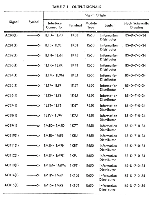
EAE Bit Assignments and Operations ... . Output S·ignals ... . Input Signals
...
.,... .
Prewired Information Distributor Connections ... . lOT Pulse Code Assignments . . . . Operator Console Indicators
Operator Console Switch Regbters ... . Operator Console Switch Controls and Indicators ... . Operator Console ManlJal Keys ... . Teletype Console Controls
...
Tape Reader Controls •••••••••••••••••••• ~ ••••••••••••••••••••• Indicator Panel Indicators •••••••••••••• e . • • • • • • • • • • • • • • • • • • • • • • •Readin Mode (R 1M) Loader Program . . . . Teletype Code
...
Maintenance Equipment ... . Maintenance Controls and Indicators ... . Power Suppl y Output Checks ... . Marginal Test Programs ... . Spare Parts for Printer Keyboard-Model KSR 33 •••••••••••••••••••• Teletype Maintenance Tools ... . PDP-7 Module List...
Suggested Spare Semiconductors . . . .Fi~ ,I 1-1
1-2
1-3
1-4
3-1
3-2
4-1
4-2
4-3
4-4
4-5
5-1
5-2
5-3
5-4
5-5
6-1
6-2
6-3
7-1
8-1
9-19-2
9-3
9-4
10-111-1
11-2
ILLUSTRATIONS
Programmed Data Processor-7 ... xvii Maior Registers, Simplified Block Diagram...
1-3
Instruction Word Format •••• oo • • • oo • • oooooooo.oooooo • • • • • • • • • • • • • • • • • • • oo. 1-10 Basic PDP-7 Cortlpone:~~ Lc>~ations ...
oo .. oo...
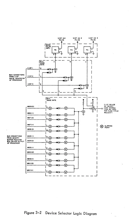
1-13 Processor Detailed Block Diagram • • • • • • • • • • • • • • • • • • • • • • e_ • • • • • • • •Device Selector Logic Diagram .... oooo • oooo oo . . . oo . . . oo.oo oooo oo. Core Memory System Rlock Diagram ... oo .. oo .... oo . . . oo . . . oo • • • • • Simple Core Memory Plane Showing Read:/\,!Vrite
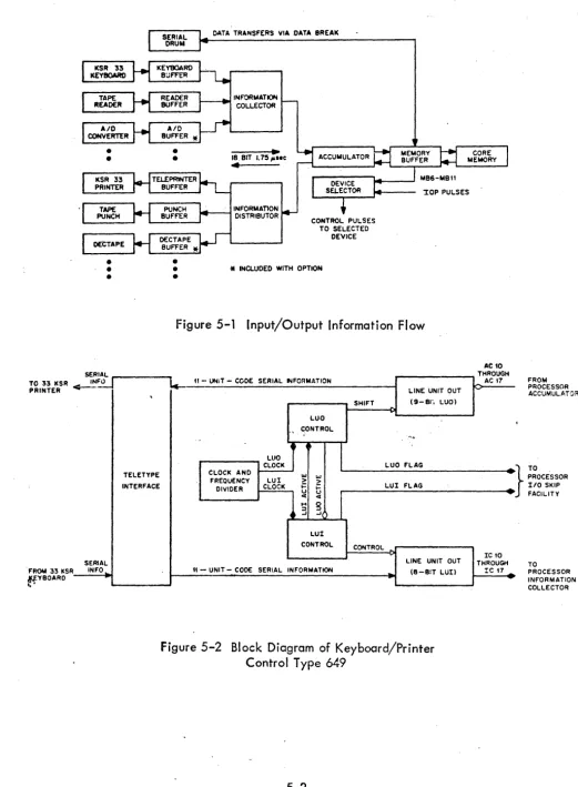
Sense, and Inhibit \"J:nriinqs .... ~ ... oo .. oo .. oo . . . . oo . . . oo . . . oo • oo . . . .. Typical Core Selection Circuit and Drive Current Path .oooo . . . oo . . . . Mern<:>ry Control Timing .. oo . . . oo . . . oo . . . . oo .. oooo . . . oo . . . oo.oo Inhibit Logic for One Memory Cell ... oooo.oo . . . oo . . . oo . . . oo • • • • oo Input/Output Informati:>n Flo"'! oo • • • • • • • • oo . . . , • • • • • • oo • • • • • • Block Diagram of Keyhoard/Printer Control Type 649 •• '.oo . . . oo . . . . Tope Format and Rcanf->r BIJff<=>1" Register Bit Assignments ... . Reader Buffer in Binary Mode ... oo • • • • • • • • • oo • . • • • • • • • • • • • . Effect of Delayed Sampl ing
Automatic
Priority Interrupt Type172
BlOCk
Diagram •••.•••
oo • • • • • • •Data
Interrupt ~Aultiplexer Tlpe173
BlockDiagram ... .
EAE Instruction Bit Assiglli1ii:~nts . . . oo • • • • • • • • • • • • • • • ' • • • • •Channel Assig:1ments for thf~ Inforrr.ation Collector ••••••.••••••••••
Installation Outl ine Drawing
...
Opera tor C~)!'$O I e
Teletype Console a _ . . . II • • • • • • • • • • • • • • • • • • •
Tape Reader - It • • • • • • • • • • • • • • • • • • • • • • • • • • • • • • • • • • • • • • • • • • • • • • •
Indicator Panel ... 0 . . . .
Marginal-Check Panel •••• ' •••••••• oo . . . oo . . . OO • • •
DEC Symbots .•..•••••.•••••••••••••.•••••••••••••••••••• " •••• Standard Negative Pu Ise
...
Figure
11-3
11-4 Drawing RS-B-728 RS-B-738 RS-B-778 RS-B-779 RS-C-739 RS-B-W505 RS-B-G800 RS-B-832 RS-C-4706 RS-C-4707 RS-C-B210 RS-C-GOO1 RS-B-G002 RS-B-G201 RS-B-G202 RS-D-G601 RS-D-G602ILLUSTRATIONS (continued)
FL IP CH IP R-Seri es Pulse •••••••••••••••••••••••••••••••• Typical DEC Logic Block Diagram ••••••••••••••••••••••••
ENGINEERING DRAWINGS
Power Suppl ies And Control
Power Suppl y (+10 and -15) ••••••••••••••••••••••••••• ' ••• Power Supply (0-20 marginal check supply) •••••••••••••••• Dual 15-Vo I t Power Suppl y •••••••••••••••••••••••••••••• Power Suppl y (one 10v and three 15v floating suppl ies) •••••• Power Supply (Memory) ••••••••••••••••••••••••••••••••• Low-Vol tage Detector (for 739) •••••••••••••••••••••••••• Control for 739 Power Supply .••••••••••••••••••••••••••• Two-Step Power Control •.•••••••••••••••••••••••••••••••
System Modules'
Eight-Bit Teletype Receiver •••••.••••••••••••••••••••••• Eight-Bit Teletype Transmitter •••.•••••••••••••••••••••••
FLIP CHIP Modules PDP-7 Accumulator
DC Sense Ampl ifier Ma5tcr Slice Control
...
In
hi
bit Dr i v er ... . Memory Selector •.••• " ••••••••••••••••••••••••••••••••• Memory Selector Matrix ••••••••••••••••••••••••••••••••• Memory Selector Matrix •••••••••••••••••••••••••••••••••WO-D-7-0-18
ML-0-7-0-19
85·-D-7-0-20
FO-0-7-0-21
85· .. 0-7-0-22
85-0-7-0-23
B5-0-7-0-24
85-0-7-0-25
85-D-7-0-26
85-0-7-0-27
8S-0-7-0-28
B5-D-7-0-2985-D-7, .. 0-30
85-0-7 -0-31
B5-0-7-0-31
B5-0-7
-0-32
85-0-7-0-33
B5-0-7 -0-34
N\l-O
-7 -0-35
BS-0-7-0-36
\ND-O-7-0-37
Cl-O-7-0-38
c:
l-D-7 -0-38
CL-O-7-0-38
Cl-D-7-0-38
'NO-O-7 -0-39
B5-D-7-0-40
ENGINEERING
DR,AWINGS
(continued)
Basic POP-7 Processor logic
Stol"dard C. P. Bus Schedu Ie ••••••••••••••••• o • • • • • • • • • • • •
Central Processor Module Map ••••••••••••••••••••••••••• Special Cycles and Key Functions •••••••• ~ •••••••••••••••• Flow Diagram ••••••••••••••••••••••••••••••••••••••••• Timing
...
Run and Special Modes •••••••••••••••••••••••••••••••••• Maior and Minor States_ •••••••••••••••••••••••••••••••••• MA, MB, arid PC Control •••••••••••••••••••••••••••••••• AC Control and link •••••••••••••••••• , __ ••••••••••••••••••. Memory Control • ' •••••••••••••••••••••••••••••••••••••••MB
Bus Drivers • o • • • • • • • • • • • • • • • • • • • • • • • • • • • • • • • • • • • • • • • •MA
andPC
Registers ... .MB Register ....•....•.•...••..•.••••..••••. ~ ••••• AC Registers (Sheet
1) "
••.••..•..•••••.•.•••••••••••••••••
P.C Registers (Sheet 2) ... . Interrupt Control •••••••••••••••••••••••••• o • • • • • • • • • • • • •
Information Col lector ••••••••••••••••••••••••••••••••••• -Information Distributor •••••••••••• _ •••• ~ ••••••••••••••••• Device Selector Module Map ••••••••••••••••••••••• " ••••• Device Selector •••••••••••••••••••••••••••••••••••••••• Console Panel Wiring Oiagram •••••••••••••••••••••••••••• CP Cables Out 1 L 1 to 1 M12 (Sheet 1)
CP Cables Out ll1 to
1 M12
(Sheet 2) CP Cables Out1 L 1
to1 M 12
(Sheet3)
CP Cables Out 1ll to
1 M12
(Sheet4)
...
Device Selector Bus Schedule ... . Central Processor Modification for EAE
xiv
11-23
11-25
11-27
11-29
11-31
11-33
11-35
11-37
11-39
11-41
11-43
11-45
11-47
11-49
11-51
11-53
11-55
11-57
11-59
11-61
11-63
11-65
11-67
11-69
11-710
11-73
ENGINEERING DRAWINGS (continued)
Drawing BS-E-149-0-4S BS-E-149-0-46 BS-E-149-0-47 BS-E-149-0-48 BS-E-149-0-49 ML-D-149-0-S0 WO-0-149-0-S1 CL-D-149-0-S2Basic PDP-7 Core Memory Logic (Type 149) Inhibit Drivers and Sense Ampl ifiers Core
Memory 0 and 1 •••••••••••••••••••••• '. • • • • • • • • • • • • • • • • • 11-77 "X 1\ Axis Selection 4K Core Memory
"Y"Axis Selection 4K Core Memory "X II Axis Selection of Core Memory "Y" Axis Selection of Core Memory
·
... .
·
....
~... .
·
... .
·
... .
11-79 11-81 11-83 11-85 Standard Memory Module Map •••••••••••••••••••••••••• ., • 11-87 Resistor Panels •••••••••••••••••••••••.•••••••••••••••• .,. 11-89 Memory Stack Connector Configuration •••••••••••••••••• .,. 11-91Basic PDP-7 Input/Output Equipment Perforated Tape Punch and Control Type 7SD
BS-0-7S0-0-2 Punch Control ••••••••••••••••••••••••••••••••••••••• '. • 11-93
Perforated Tape Reader and Control Type 4MB
BS-0-444B-0-2 ML-0-444B-0-3 WO-0-444 B-O-S
Reader Control ••••••••••••••••••••••••••••••••••••••••• Reader 444B and Punch 7SD t-Aodule Map ••••••••••••••••••• Reader 444B and Punch 7S0 Bus Schedule
...
Teletype Control Type 649
85-0-649-0-2 Keyboard/Printer Control
...
POP-7 Options Extended Arithmetic Element Type 177
FO-0-177-0-2 FD-0-177-0-2 FO-D-177-0-3 85-0-177 -0-4
EAE Flow Diagram (Sheet 1) •••••••••••••••••••••••••••••• EAE Flow Diagram (Sheet 2) ••••••••••••••••••••••••••••••
EAE Modul
~Mop
... "
... .
EAE States
...
ENGINEERING DRAWINGS (continued)
Drawing85-0-177-0-5
85-0-177-0-6
85·-0-177 -0-7
85-0-177-0-8
85-0-177-0-9
Cl.-D-177-0-10WD-0-177-0-12
PDP-7 Options (continued)
EAE Step Counter and Control ... oo . . . . EAE Register Control ... oooo . . . oo .. oooo.oo • • • • • oo • • oooooooooooooo Main Time Chain oo.oo.oo .... oooo oo.oo oooo . . . oooooo.oooooooo • • oooooo.oooo.oooooo.
MQ Register .. oooo.oo.oo . . . oo . . . . oo • • oo . . . oooooooo . . . . oo.oo . . . . oo. AC Inverters .. oo . . . oo • • • • oo .. oo • • • oo.oooo.oooo . . . oo • • • oo . . . oo • •
EAE Cable Schedules ... . Pin and Block Layout EAE oooo.oooo .... oo . . . oo .. oo .. oooo .. oooo .. oo .... oooo . . . oo ....
Data Interrupt Multiplexer Type 173
8S-0-173-0-2
85-0-173-0-3
ML-D-173-0-5
WO-0-173-0-8
Data Interrupt Multiplexer Control
...
Data Interrupt Multiplexer DataInput/Data Addresses ... ..
Data InterruF't Multiplexer Module ivi\ap .. oo . . . oo . . . oo . . . . oo . . . . 8us Schedu Ie ... .. . .
~utomatic Priority Interrupt Type 172
85-0-172-0-2
85-0-172-0-3
85-0-172-0-3
ML-D-172-0-5
WO-D-
172-0-6
Automatic Priority Interrupt Control ... oo.oooo . . . oooooo Automatic Priority Interrupt System (Sheet 1) ... oo . . . .. Automatic Priority Interrupt System (Sheet 2)
...
Module Map ... oo . . . oooo .. oo . . . oooo .. oo . . . . Pin and Block Layout ... ~ •11-111
11-113
11-115
11-117
11-119
11-121
11-123
11-125
11-127
11 .. ·l:!9
':;;;;~~~:,~,~~ci=
r-ii,~~'i_,~""~~~j-.
1
t.
'-'~ ,''111
[image:18.615.62.557.40.662.2]CHAPTER 1
INTRODUCTION AND
DESCRIPTION
The Digital Equipment Corporation (DEC) Programmed Data Frocessor-7 (PDP-7) is a general purpose, stored-program, solid-state digitol computer designed for use in laborotories, com-puting centers, or process control systems. The PDP-7 is single-address, fixed l8-bit word~ length, ~i nary computer using l's compl ement arithmetic and 2's compl ement notation to facilitate multiprecision arithmetic. A basic PDP-7 contains a 4096- or 8192-word, random access, ferrite-core memory which can be expanded in increments of4096 words to a maximum ca-pacity'of 32,768 words by the use of additional memory modules and a DEC Type 148 Core MemoryE:dension Control. High-capacity, flexible input/output circuits permit the computer to operate with all modern types of data processing equ ipment and many types of process-control
instrument,s.
The basic PDP-7 includes the processor {with operator console}, 4096-word core memory, input/output control with a device selector that permits selection of up to 64 I/O devices and is expandable, information collector, information distributor, and real-time clock. 4 The pro-cessor provides
fa~iI
Hies for program interrupt, data interrupt {for use with high-speed I/Odevices},
I/O
status check,I/O
skip, andI/O
trap (which provides the basic hardware nec-essary for a time-shared or multiuser system). The input/output equipment supplied with a basic PDp·-7 system consists of a high-speed perforated tape reader (300 char/sec); a high-speed paper tape punch (63.3 char/sec); and a Model 33 KSR Teletype unit {l0 char/sec}.The PDP-7 is completely self-contained and requires no special power sources, air-conditioning, o'r floor bracing. The PDP-7 draws its primary power from a single source of l15v, 60-cps, single-phase power, and from this source produces all required operating voltages. Upon re-quest, PDP-7 systems can be supplied to operate from 220v, 50-or 60-cps supplies. Built-in provisions for vary;ing the
+
10 and -15v suppl ies that power the logic permit the operation of the logic to be checked under marginal conditions. The computer is constructed with standardDEC FLIP CHlp™ modules and power supplies.
TMFLIP CHIP is a trademark of the Digital Equipment Corporation
This manual provides information required for maintaining a basic PDP-7 system. The manual also provides information concerning the following commonly used options: Type 177 Extended ArIthmetic Element, Type 172 Automatic Priority Interrupt, and Type 173 Data Interrupt
Multi-plE~xer •
COMPUTER ORGANIZATION
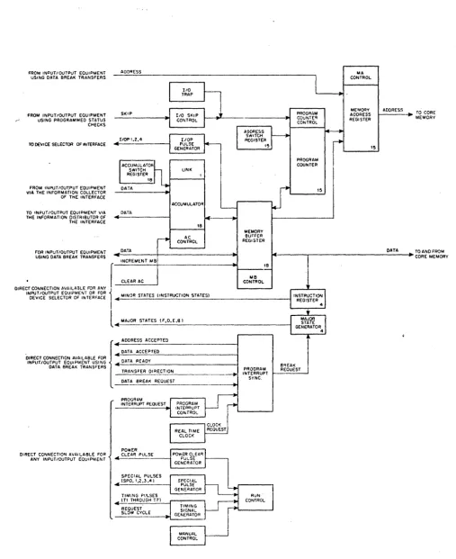
The computer consists of a processor (with operator console), a core memory, interface equip-ment, and input/output equipment. Figure 1-2'illustrates the interrelationship of these
elements. All arithmetic, logic, and system control operations are performed by the processor. Te,mporary information storage is provided by the various registers of the processor 'and by asso-ciated input/output devices. Permanent information storage (longer than one instruction time) is provided by the core memory. During each computer cycl e lasting 1 .75 fJsec, the core
m~emory automatically performs a read operation and a write operation under the control of timing signals produced by the processor. Interface circuits permit connections to a variety of peripheral equipment, and are responsible for detecting all I/O select codes and for provid-ing necessary input or output gatprovid-ing. Individually programmed data transfers between the pro-cessor and peripheral equipment take place through the accumulator. The data break faci! it>,
p~~rmits single or multiple data transfers to be initiated by a high-speed I/O device; each transfer using ,the data break is completed in a single computer cycle. The interface circuits also permit peripheral equipment to perform certain control functions, such as instruction skip-ping or the initiation of a program interrupt to transfer program control.
Processor
The processor performs logical and arithmetic functions, controls the storage and retrieval of in-fc)rmation on core memory and controls the flow of information to and from peripheral equipment. The processor consists of control logic and six major registers. Associated with the processor is the operator console, which permits the information contents of memory and of the major registers tc) be manually established, modified, or examined.
-n
mO
e .., CI) I "->S
0 0..,
:;:0 CI) CO VI -CI)i
..,
Vlw '"
Vl
-.
3 -0-.
-t-\ in" c.. OJ 0 0 A 0-.
0(Q ..,
0
3
1
-AOORESS
- - - I
, - - ,
CONNECTION TO INPUT/OUTPUT ~I
"'""" I
I .... ",
I
I'EQUIPMENT USING THE DATA OATA
8REA~ ~~~---r-r---~ tf81~~~~ ~I
LINK I~
~
ATACONNE(TlO~j TO STANDARD - - -
I. .
.-1 ACCUMULATOR AND OPT:ONAL INlJiJT I OUTPUT[QUIP ... n~T USING PROG'lAMMED CONT~
(lATA TRANSFEfiS . . - . I
~E~E.-l
18 18
MAJOR STATE GENERATOR INSTRUCTION REGISTER 4
I PROCESSOR _ _ _ _
L - - - - -
-r- - - - -
r - - _ -.-.1I
I
r -:--
-1- .. - - - ... - -----I
--L
I
t-~l
I I I REGISTER SWITCHES~EYS aMOO£ SWITCHES REGISTER INDICATORS I I I I
I ' " " , 1
Accumulator (AC) and Link (L)
The
AC
is an l8-bit register which performs arithmetic and logical operations on the data and serves as a transfer register for programmed information transfers between core memory and peripheral equipment. The link isa l-bit register which extends the arithmetic facility of theAC
and simplifies the programming of arithmetic operations. The link serves primarily as a carry or overflow register for the AC.Memory Address Register (MA)
This 13-bit register holds the address of the core memory location currently being ~sed. Two additional bits are wired into the basic PDP-7 but are used only if the memory storage capacity
is extended beyond 8192 words by means of the memory extension options.
Memory Buffer Register (MB)
This la-bit register serves as a buffer for all information passing to or from core memory from the processor or external devices using the data break.
Instruction Register (lR)
This 4-bit register holds the operation code of the instruction currently being performed.
Program Counter (PC)
This l3-bit register holds the address of the memory location from which the next instruction is
to be taken.
As
in theMA,
two "additional bits are provided, but are used only in conjunction with the memory extension options.N\ajor State Generator
The major state generator is a multistate device which can assume anyone of four stable states, each corresponding to one of the fO'Jr major control states of the processor. One or more states are entered to execute a programmed instruction, but only one state exists at anyone time.
Operator Consol e
All.
manual controls and all processor readouts and indicators are located on the operator console. The!e may be classified as follows:1. Register switches, used to preset a binary number for transfer into an associated register. To facilitate presetting numbers specified in octal notation, the switches assoc iated with each register are grouped in threes. The order of significance is from right (least significant) to left {most sig-nificant} •
2.
Keys and mode switches, used to initiate specific computer functions.3. Register indicators, used to display the contents of an assoc iated reg-ister. A lighted indicator lamp denotes a binary 1 in the associated bit of the register.
4. Pr imary power sw itc hes .
Core Memory
The high-·speed random-access core memory of the basic PDP-7 is a 4096-word coincident-current core module with a read/write cycle time of 1.75 IJsec. In each cycle, the memory reads an l8-bit word stored in the memory location specified by the MA, transfers the word into the MB, and rewrites the word into the same memory location. Extension of the core memory capacity to 8192 words may be accompl ished merely by the addition of another 4K memory module, and requires no modifications to the processor. Extension of memory capacity beyond 8K requires the use of the memory extension options {memory modules and memory ex-tension control}.
Interface
The interface control I inks the processor to input and output stations, calls the stations, and collects and distributes the input/output data. It also controls the interleaving of high-speed data transfers between programmed instructions during the data break {cycle stealing}; senses
the status of I/O devices and permits the status sensed to cause an instruction to be skipped;" inaiates program control transfers; and, in multiuser or time-shared systems, traps illegal in-struct ions.
No additional interface equipment is required for the connection of standard DEC peripheral equipment to the PDP-7. If special-purpose devices are to be connected to the PDP-7, a suitable interface may easily be constructed using the standard I ine of FL IP CH IP modules manufactured by DEC.
Input/Output
The standard input/output equipment provided with a basic PDP-7 consists of a Model 33 KSR Teletype unit and DEC Type 649 Teletype Control, a Digitronics Type 2500 Perforated Paper TClpe Reader and DEC Type 444B Reader Control, and a Teletype BRPE Perforated Tape Punch and DEC Type 750 Punch Control.
T1eletype and Control
The Teletype unit is a standard machine operating from serial ll-unit code characters at a rate of 10 char/sec. The Teletype provides a means of supplying dota to the computer by means of a keyboard, and of typing output data from the computer on a page-size paper roll. The Teletype control converts serial characters from the keyboard into parallel form for acceptance by the computer, and converts para II el computer output data into serial form for acceptance by the printer. The keyboard and printer, and their associated control circuits, form two separate and distinct information channels, thol.,lgh information typed on the keyboard is always printed by the printer.
!)erforated Paper Tape Reader and Control
The reader senses information contained on 8-channel, fanfold paper tape photoelectrically, (It a rate of 300 char/sec. The control contains a data register, a flag, and Jogic circuits which permi t reader operation to be controlled by the stored program ..
Perforated Paper Tape Punch and Control
The high-speed paper tape punch perforates a-channel, fanfold paper tape at the rate of 63.3 char/sec. The control contains a dato register, a flag, and control logic. All punching operations are performed under the control of the stored program.
Processor Options
The processor options described in this manual are the Type 177 Extended Arithmetic Element I
The Type 172 Automatic Priority Interrupt, and the Type 173 Data Interrupt Multiplexer.
Extended Arithmetic Element
The extended arithmetic element (EAE) facilitates high-speed multiplication, division, shifting, normal izing, and register manipulation. Installation of the EAE adds an l8-bit mul tipl ier-quotient register (MQ) and a 6-bit step counter register (SC) to the computer. The contents of the MQ are continuously displayed on the operator console. The EAE operates asynchronously with resp€~ct to the computer cycl e, thereby permitting computations to be pe:-formed in the minimum possible time. Further, EAE ;nstructions ar€: microcoded so that several operation~
can be performed by one instruction. Average multiplication time is 6.1 llsec, average division time is 9 ~sec.
Automatic Priority Interrupt
The automatic priority interrupt (API) inCf€::lSeS the caparity of the PDP-7 to handle data trans-fers of information to and from I/O devices
by
directly identifying an interrupting device without the need to scan flags. The API is particularly useful in ensuring rapid servicing ofI/O devices which retain their information for a limited period {such as the real-time clock or analog-to-digital converters}. The API provides 16 automatic interrupt channels arranged in a priority sequence in which channel
Os
has thehighest priority and channel 178 the lowest. The priority chain guarantees that if two or more I/O devices request an interrupt concurrently, the first interrupt is granted to the device with the highest priority. The requests of the other devices are registered and are later serviced in order of priority. Multilevel interrupts are permissible, where a device of higher priority supersede!; an interrupt already in progress.Data Interrupt Multiplexer
The- data interrupt multiplexer permits the single data break facil ity of the PDP-7 to be used
by up to four high-speed I/O devices. Each devi ce must supply 18 data lines, 15 address lines, a h'onsfer direction signal, and a break request signal. When a data break is granted by the processor, each informatio., transfer is completed within one computer cycle. The maximum combined transfer rate is 570,000 l8-bit words/sec.
FUNCTIONAL DESCRIPTION
Th,e PDP-7 performs arithmetic or logical operations upon data stored in the core memory. The nature and sequence of these operations is determined either by a series of instructions, also stored in memory (programmed operation), or by operation of keys and switches on the operator console (manual operation). Manual operation is restricted to the following: starting and stop-ping programmed operation; continuing programmed operation after a temporary halt; setting the starting address (memory location) of a program into the memory address register; depositing
information in manually selected memory cells; examining the contents of manually selected memory cells; and the ;;election of special modes. For mointenance or debugging purposes, 0
de~posit or examine operation may be repeated manually to permitvisual monitoring by means of the register ind icator lamps on the operator console or bysignal tracing with an oscilloscope.
During programmed operation, the processor retrieves from memory the first instruction specified
by
the program, executes the instruction during one or more computer cycles (each cycle lasting 1 ,,75 ~sec), and then proceeds to retrieve and execute the remaining instructions specified by the program sequence. All arithmetic, logical, or control operations of which the computer is capable are performed as a function of three major determinants: the instruction 'retrieved from memory; the major control state establ ished; and timing pulses produced by the processor.Instructions
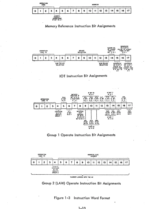
Instructions are of two types: memory reference and augmented. All instructions contoin an operation code (specifying the nature of the instruction) in bits
°
through 3.Memory reference instructions cause information to be stored in or retrieved from memory, and contain a memory address as well as an operation code. All memory reference instructions
require one computer cycle in which the instruction is retrieved, and all except the jump
instructiorl require a second cycle in which to execute the instruction specified by the operation code. The jump does not cause storage or retrieval of information, but transfers control of the processor from one block of consecutive memory locations (containing instructions) to a different block of consecutive locations. The jump instruction is normally completed in one computer cycle. If indirect addressing is employed, two cycles are required for the jump and three cycles for other memory reference instructions.
Augmented instructions do not require reference to memory. Since no address is required, bits 4 through 17 are decoded to initiate various operations to extend or augment the operation code. Because no storage or retrieval operations are performed, most augmented instructions can be completed in one computer cycle. Augmented instructions are divided into three classes:
1. Instructions having an operation code of 648 are EAE instructions. 2. Instructions having an operation code of 708 are input/output transfer (lOT) commands, and are used to control or test the status of I/O devices, or to effect an informatio~ transfer.
3. Instructions havi ng an operation code of 748 are operate (OPR) commands, and are used for basic processor data manipulation such as instruction skipping as a function of register condition, shifting, rotating, etc.
The formats of the various types of instruction words are ill ustrated in Figure
1-3:
Appendix 1 contains'a list of the instructions performed by the PDP-7.Major Control States
The computer operates in one of four major control states during each machine timing cycle. One or more states are entered to execute an instruction. The states are fetch, execute, defer, and break and are determined by the major statE~ generator. Only one state exists at a time and all states, except break, are determined by the programmed instruction being executed.
o OPPATIOH COO[ '--...-' INOIRECT AOORtSS~
• &IT 15 A ,
6 7
ADOAESS
9
10 " 12 113 114115116117
i
Memory Reference Instruction Bit Assignments
OPERATION
CODE 70 SELECTION DEVICE
.
GENERATE CLEAR Ae AN ItOP 2 AT EVENT PULSE AT EvENT TIUE , IF TIME 2 IF BIT 81T IS A 1 IS A I
r
,0 1 2'--...---'
SUB-OEVICE SELECTION
7 8 9
~ ,.-..J--..
10 11
, I '--r--'
SUB-DEVICE GENERATE SELECTION AN 1/01' 4 PULSE AT EVENT TIME
4 IF BIT IS AI
lOT Instruction Bit Assignments
'iF liT e IF' BIT 7 I'IOTAT£ I IS A I IS A t
GENF.RATE AN I10P I PULSE AT EVEItT TIME
I IF BIT 15
A I
CLA ~~I;~O: %. / SZL S~A SPA' MLT I RTA ' ATL ' CIIIL OPEJUTION IF BIT Z POSITIONS IF BIT IF BIT I' BIT IF BIT IF BIT IF BIT IF BIT
coer.:: 74 IS A , IF A' IS A I IS A , IS A I IS A I IS A 1 IS A , IS A I
, ----. ,..-... .--'---, ...--'---.,.--"--..~,--)-,~ ~
r?
i '
I 2 I 314
I~
I 6 I 7i
8i
9 110 j " jl2 I 13 I 141,5i
16 1'7""--v-' ~
n
---...--'~~ ~10
OPERATION COOE 74
2
CONTAINS CLL REVERSE RAR RAL OAS eMA A 0 TO IF BIT SKIP IF BIT IF BIT IF BIT IF BIT
:,.~~~ IS A I ~~Nill~ .15 A I IS A " IS A 1 ISA 1
9.10." If IF ~T 7
BIT II IS A I IS A 0 SNL 52A SUA
If BIT If BIT IF BIT
,r5AO 15:0 IS 1.0, IF 81T I IS A 0
Group 1 Operate Instruction Bit Assignments
6 7 8
AOORESS SIZE NUMBER
9
110
1"
112
1
,3I
141
,5 16 17 \-...;--'CONTAINS
AlTO SPEClry
Gfl04P 2
~~---y---~
NUMBER LOADED INTO THE At
Group 2 (LAW) Operate Instruction Bit Assignments
Figure 1-3 Instruction Word Format
[image:28.629.35.551.45.765.2]Fetch (F)
A new instruction is obtained when this state is entered. The contents of the memory cell specified by the PC are placed in the MB, and the operation code (bits 0-3) of this instruction word is placed in the
IR.
The contents of thePC
are then incremented by1.
If
a single-cycl e instruction is fetched, the operations specified are performed during the last part of the fetch cycle; then the next cycle is a fetch state for the next instruction. If a 2-cycle instruction is fetched, the succeeding control state is either defer or execute.Defer (D)
When bit 40f a memory reference instruction is a 1 I the defer state is entered following the fetch
state I to perform the indirect addressing. The memory location addressed by the instruction contains the address of the operand I and access to the operand is deferred to the next memory cycle (execute).
Execute (FJ
This state is established only when a memory reference instruction is being executed. The con-tents of the memory cell addressed are brought in'to the ~AB; and the operation specified by thl? contents of the
IR
is performed.Break (B)
'Nhen this state is establ ished , the sequence of instructions is broken for a data interrupt or a program interrupt. In both cases, the break occurs only at the completion of the current in-struction. The data break interrupt allows information to be transferred between" core memory and an external device. When this transfer has been completed, the program sequence is re-sumed from the point of the break. The program interrupt causes the sequences to be altered. The contents of the PC and the contents of the I ink are stored in core memory location 0000, a'nd the program continues from location 0001 .
Tin:'ing
Seven times (designated T1 through T7) occur in sequence during each computer cycl e. At each time, two pulses are generated, of which one is 40 nsec and the other is 70 nsec wide.
ThE~se time pulses cause gating circuits to perform seque'"!tial or synchronized logical or control opE3rations. The narrow pulses are used for operations where timing is critical, such as the simultaneous sampling and incrementing of a register; the wider pulses are used to initiate gating operating where timing is less critical. The intervals between successive pairs of timing pulses permit gates and registers to settle before any new operation is initiated,. During each computer cycle, memory reading occurs between times
T2
andT3;
memory writing starts at time T4 and occupies the remaining portion of the cycle.PHYSICAL DESCRIPTION
The basic PDP-7 is housed in three standard DEC metal computer cabinets bolted together to form an' intergrated console. In each cabinet, double doors at the front (held closed by mag-netic latches) provide access to the wiring side of
all
module mounting panels. Double rear doors provide access to a plenum door on which the power supplies are mounted; the plenum door is latched by a spring-loaded pin at the top. Opening the pi enum door permits access to the modules. A fen, mounted in the bottom of each cabinet, draws air through a dust filter to coot the modu t es. The a irstream passes over the modul es and is exhausted through louvered openings in the top of the cabinet I at the front. Four casters permitralobil
ity of the computer.Figure 1-4 shows the locations of components in the basic PDP-7. Note that the perforated tape reader and punch are mounted in the center bay above the operator consol e. The Teletype unit may be mounted on its own stand (suppl ied with the equipment) or may be placed on the c()nsole table. For additional physical data, refer to the table of physical data given below,
and to the Installation section of this manual.
Cabinet He ight Cabinet Vlidth Table Width Cabinet Depth Table Depth
SPECIFICATIONS
Physical
69-1/8 inc hes 61-3/4 inches 68-15/16 inches
33-9/32
inches19-7/8 inches
BAY 3 BAY 2 BAY
,
BAY I BAY 2 BAY 3. "
-.
POWER SUPPLY
(Q
C 738 BLANK
""l r.. _ ..
-CD POWER SUPPLY
778
TRIPLE fAN
INDICATOR PAP~EL BLANK INDICATOR PANEl 8LANK
A MARGINAL CHECK
I-a MEMORY LOGIC AIR BAffLE PANEL PANEL
I MOUNT ING PANEL
~ (REMOVE.D fOR leK OR MORE Of
BLANK CORE M[MORYI
C
0
': MEMORY ARRAY
I-PERfORATED
CP SYSTEMS MODULES
0 MOUNTING PANEL BLANK
~.
0 - - - 8LAII.K 1--. _ _ ...
-TR,PLE FAPl
-0 POWER SllF'Pl Y - - - ... OUNTING PAIIIEL
0 SYSTEMS MQOUt .. £S (k(MQV[O FOR 16K 728 MOUNTING fANlL AN~ OR MOHr o~
-0 TELETYPE DHIVER CORf MeMORYl
I 1 .
-"I
---_
.. - - -... ---- TRIPL£ fANW BL.ANK OJ( ~o CYCLE MOUNTING PANEL
() STfPOOWN
f---0 PO;l;(H SUPPLY 1 RAN·;fOHMUI POWER SUPPLY
f PUNCH TAPE
I - r--
-H
~ ME MORY LOGIC
-J
II
~''''''''''
J~I
I
A 1A"'E-a
-
!\
READER\ r
- - - - BLANK -.
C
-
-D OPlRATOR
l CO,,"SOL£
-3 179 ---_._--- 728 r
PROCESSOR ' - - - - i t - a , _ E
-0 BLANK
0
::J
lOGIC
-H
f--
-J
(!) BLANK
::J POVlE~ CONTROL POWER SUPPLY
-
8~2 728 POWER SUPPLY MEMORYr- 739
.
01---.-n
0 8LANK BLANK
I(
f-
-l
M ~ II PEF/fORATED TAPr.
~
-
-
R(ADfR/PUNCH-IN !l OEVICE Sf.LEC10R !l CONTHOl lOGiC ANO I/JlMJAl CO'HROl
--
o·
'---::J
I
c rUNC liONS lOGIC 828
BLANK
-
POWER0 R[CEPTACL(
CII
U U U U
Cabinet Door CI earance Cabinet Weight (3 cabinets) Teletype Height
Teletype Width Tel etype Depth Teletype Weight
Power Requirements
Power Dissipation Digital Signal Levels
Operating
T
empercture Operating Humidity Storage Temperature Storage Hum i di ty Heat DissipationCycle Time Word Length Core Memory Size
Instructions
14-7/8 inches at back 1100 Ibs
8-3/8 inches 18-5/8 inches 18-1/2 inches 40lbs
Electrical
115v, 60 cps, single phase, 17 amp for standard PDP-7 (can be constructed for 220v or 50 cps upon spec ial request)
2200w
ground and - 3v
Ambient Conditions 50 to 1220 F
o
to 90% re lative hum idity32 to 1220 F
less than 90% 7150 Btu/hr
Functional 1 .75 tJsec 18 bits
4096 or 8192 words, expandable to 32,768 in increments of 4096 words.
16 basic instructions (13 memory reference and 3 augmented). The augmented instructions are microprogrammed to produce more than
1 75 commands.
Input/Output Capability 64 different devices can be individually selected and addressed by 3command pulses.
PERTINENT DOCUMENTS
Publications
The following publ ications serve as source material and compl ement the information in this manual.
1. Digital FLIP CHIP Modules catalog, C-105, printed by DEC. This book presents information pertaining to the function and spec ifications of the FLIP CHIP modules and module accessories used in the PDP-7.
2.
System Modules catalog, C-100, printed by DEC. This book presents information pertaining to the function and specifications of the basic system modules and module accessories used in the PDP-7.3.
Programmed Data Processor-7 Users Handbook, F75~ printed byDeC.
Programming, instruction format, an"d genera
I
computer function are presented in this document.4.
PDP-7 Software Package. Perforated program tapes and descriptive matter for the Program Assembly language {PAL}, utility subroutines, and t'he maintenance programs {Maindec} are contained in this package prepared by DEC. The content of the package is listed in Table 1-1.5.
Instruction manuals and Maindec programs for appropriate input/output devices are prepared by DEC.6. Technical Manual, Keyboard Send and Receive Sets (KSR), Bulletin 273B
(Vols. 1 and
2).
This manual covers operation and maintenance of the Tele~ type unit.7. Parts, Model 33 Page Printer Set, Bulletin 1184B. This illustrated parts breakdown can be used as a guide to disassembly, reassembly, and ordering parts of the Tel etype un it.
8. Technical Manual, High-Speed Tape Punch Set (BRPE), Bulletin 215B. This manual covers operation and maintenance of the tape punch unit.
9. Parts, High-Speed Punch Tape Set (BRPE), Bulletin 1154B. This illus-trated parts breakdown can be used as a guide to disassembly, reassembly, and ordering parts of the tape punch un it.
10. Digitronics Perforated Tape Reader Model 2500 manual. This book covers the installation, use, theory of operation, and maintenance of the tape reader un it .
TABLE 1-1 PROGRAM LIBRARY
Number Name Number
Name
Dig i to 1-7- 1-S Symbolic Tape Editor Digital-7-23-10 Buffered Input/
Dig ita t -7-2 - S FORTRAN 11 System - Output Package
8K Digital-7-24-10 Pen Follow
Sub-Digital-7-3-S Assembler - Basic routine
and Extended Digital-7-25-10 Character Display
Digital-7-4-S DDT (Debugging Tape) Subroutine
Digital-7-10-0 Teletype Output Digital-7-30-A Floating Point
Package Package
Dig ita 1-7- 1 1- 1 0 Tic Toe Digital-7-31-A Multiply Subroutine Digital-7-12-1 F F Loader Digitol-7-32-A Divide Subroutine Digital-7-13-1 Readin Mode Loader Digital-7-33-A Double Precision
Integer Package Digital-7-14-0 Octal Print Subroutine
Digital-7-34-A Unsigned Mul tiply
Digital-7-15-0 Decimal Integer Print Subroutine
Digital-7-20-10 . PDP-7 DECtog Digital-7-35-A Unsigned Divide
Digital-7-21-10 PDP-7 DECtrieve Subroutine
Digital-7-22-10 PDP-7 DECtape Digital-7-40-U Master Tape
Dupli-Subroutine cator
TABLE 1-1 PROGRAM LIBRARY (continued)
Number Name Number Name
Digital·-7-41-U Tape Reproducer Digital-7-53-M Reader and Punch
Digital-7-43-U CAL Handler Type I Test
Digitol-7-44-U CAL Handler Type III D i gi ta 1-7-54-M Maindec 401
(Instruction Test) Digital-7-45-M Type 57A Compiler
Digital-7-55-M Maindec 402
Digital·-7-50-M Tel eprinter Input/ (Checkerboard)
Output Test
Digital-7-56-M Maindec 403
Dig ita 1-7-51-M Clock Interrupt (Address Test)
Test Program
Digital-7-57-M Maindec 410
Digital-7-52-M CONTEST II (RPB Test)
One copy each of publ ications 3 through lOis suppl ied with each PDP-7 system. Copies of . items 1 or 2 or additional copies of items
3
through 10 can be obtained from the nearest DEC district office or from:Field Service Department Digital Equipment Corporation 146 Main Street
Maynard, Massachusetts 01754
U. S. A.
Additional copies of items 6 through 9 can be procured from: Teletype Corporation
5555 Touhy Avenue Skokie, Illinois 60076 U.S.A.
The engineering drawings I isted in the table of contents are reproduced in Section 11 as an aid to understanding and maintaining the PDP-7. All the logic diagrams are included, but schematics are given only for those modules nof' described in the DEC System or FLIP CHIP
[image:35.615.54.570.25.335.2]Module Catalogs. A complete set of formal engineering drawings and module schematics is. supplied separately with each PDP-7 system. Should any discrepancy exist between the
draw-ings in this manual and those suppl ied with the equ ipment, assume the formal drawdraw-ings to b~ correct.
ABBREVIATIONS
Listed below are the most commonly used abbreviations of registers, key operations, components, il1structions, and signal names. Instruction mnemonics not included in this list will be found in Appendix 1, Instruction Summary. Signal names not included in this list will be found in Appendix 3, Signal Glosser}' ~ This appendix contains an alphanumerical I ist of all signal names which appear on the engineering drawings, together with the number of the drawingo.n which each signal is generated.
AC Accumu I atar CRY Carry
ACS Accumulator Switches CY or CYC Cycle
ADDR
Address 0 Defer {state}API
Automatic Priority DA Data AddressI nterrlJpt
DAC Deposit Accumulator
AS Address Switches Contents
I~ Break {state} DCD Diode-Capac itor- Diode
I~D Bus Driver Gate
I~GN Begin 01 Data Information
BK RQ Break Request DIV Divide
C Complement DLY Delay
CAL Call Subroutine DP Deposit
CHAN REQ Channel Request OS Device Set ector
CHAR Character DPN Deposit Next
CLA Clear Accumulator E Execute {state}
CLK Clock EAE Extended Arithmetic
Element
CLR Clear
EMA Extended Memory Address
CONT Continue Register
CP Central Processor EMB Extended Memory Buffer
Register
EN or ENB Enable OP Output
EPC Extended Program Counter OPR Operate (class of
instruc-EX Examine tion)
EXN Examine Next OV Overflow
F Fetch (state) PA Pulse Ampl ifier
FLG Flag PB Punch Buffer Register
HLT Halt PC Program Counter'
Ie Information Coil ector PI Program Interrupt
10
Information Distributor PIC Program Interrupt ControlINH Inhib it PIE Program Interrupt Enable
INT RQ Interrupt Request POV Possible Overflow
INVTD Inverted PROG Program
I/OP Input/Output Pulse PUN Punch (tape)
lOT Input/Output (information) PWR ClK Power Clock
Transfer PWR ClR Power Clear
IR
Instruction Register RB Reader Buffer RegisterISZ
Index and Skip if Zero RD FLG Reader Flag(i nstruct i on)
RDR Reader
JMP Jump (instruction)
RPT Read Paper Tape
JMS Jump to Subroutine
RQ Request
(instruction)
KBD Keyboard RTN Return
L
Link SA Sense AmplifierLAC Load Accumulator SAD Skip if Accumulat<:>r Differs
LUI Line Unit In (Teletype SEL Select
keyboard buffer) SKP Skip
LUO Line Un it Out (Teletype SP Special Pulse
pr inter buffer)
STS Strobe
MA Memory Address Register
SW Switch
MB
Memory Buffer RegisterSYNC Synchronize
MQ Multipl ier Quotient
TAD Two's Complement Add
Register
MS
Major States T Timing Pulse (70-nsec)MUL ~ultiply TP Timing Pulse (40-nsec)
XCT XOR
Execute (instruct ion) Exclusive OR
SYMBOLS AND TERMINOLOGY
Digital Logical Symbols
A complete I ist of thedig'ital logic symbols used in the engineering drawings of this manual ccm be found in Appendix 1 •
Conventions and Notations
Conventions and notations on engineering drawings and in text describing the PDP-7 are used as follows:
V
¥
A
:9
+
--+
Programming notation for the inclusive OR function. Programming notation for the exclusive OR function. Programming notation for the AND function.
Programming notation for an information transfer.
Design notation for the inc lusive OR function and program notation for addition. Design notation for the AND function.
Design notation for an information transfer accompl ished by a single signal (used without parentheses).
( ) The contents of a storage device.
C(A) VC(B):#>C(A) The contents of register B are OR combined with the contents of register A orA V B =>A
A2(1)orA~
+ 1 - + A
O~A
A~B
and the result is stored in register A.
Bit 2 of register A is the state corresponding to a binary 1, or contains a 1 • The contents of register A are incremented by 1 •
Register A is cleared or set to contain all O's.
The content·s of register A are jam transferred into register B. Other terms used in this manual are defined as follows:
absolute address - a number used directly to specify any memory location. Twelve bits are required to address 4K, 13 bits to address SK, 14 bits to address 16K, and 15 bits to address' 32K.
address of the operand - the location of a core memory register currentl y containing the operand.
clear - to clear a register is to establish the state corresponding to binary 0 in all bits of that register.
:Iock break - an interruption of the main program, lasting one computer cycle. During this cycle, a real time clock increments the contents of memory location 78 by 1. When the clock is enabled by a programmed instruction, a clock break occurs every 1/60 sec. If memory location 78 c)verflows, the clock flag is set and may cause a program break •
. command - a signal that causes a specific operation to occur as the complete or partial execution of an instruction or microinstruction.
~yc1e stealing - a suspension of the main program for one computer cycle caused by the clock break or data break facil ities to effect an operation or transfer information with ~ore memory.
,data break - an interruption of the main program lasting one computer cycle. During this cycle an information transfer takes place between core memory and a high-speed I/O device. The data break is requested by the
I/O device when it is ready for .the transfer, and the break occurs as s~on as the processor reaches an II instruct ion done" situation.
effective address - the address of the operand as specified by an instruction word or by an absol ute address.
flag - a fl ip-flop or signal that indicates a specific equipment status or condition. Flag signals are used to identify an I/O device which requires servic ing, as. well as for other purposes.
instruction - an l8-bit word which is stored in memory and is identified by a distinct operation code in the four most significant bits. When retrieved from memory, an instruction word causes specific operations to be performed by the processor.
microinstruction _. a command to perform a specific operation, identified by the placement of lIs and O· j in bits of an instruction word other than those
which contain the operation code. Several microinstructions can be com-bined within a singl e instruction word. In effect, the entire word is used as an operation code, and is decoded by gati.ng circuits within the processor to produce mul tipl e command pulses.
operand - a stored binary number to be operated upon.
program interrupt - an interruption of the main program initiated by peripheral equipment which requires servicing. When the processor reaches an lIinstruc-tion done" situalIinstruc-tion, control of the processor is transferred to a subroutine which identifies the interrupting device. The transfer of cor-trol takes place during the break cycle. After the interrupting device has been identified,. a further subroutine services it and then transfers control of the processor back to the main program.
set - to set a flip-flop is to establ ish the state corresponging to binary 1 •
subroutine - a series of stored instructions which is not part of the main pro-gram but may be reached by means of a JMS instruction. A subroutine may contain instructions that service peripheral equipment, or instructions for an operation that must be repeated many times. At the conclusion of a sub-routine, control of the processor may be returned to the main program.
CHAPTER 2
LOGIC
FUNCTIONS
Both manual and programmed operation of the PDP-7 are required for the performance of any complete task. Manual operation is normally limited to the following: storing a br.ief loader program; modifying or exam ining data or addresses in a program that is already stored; or establishing the starting conditions for programmed operation. In programmed operation, data and the sequence of 'instructions which constitutes the program are loaded into the core memory; the starting address of the program is manually established; and the computer is manually started. The computer then successively executes the instructions specified by the program. For main-tenance purposes and to facilitate debugging, provision is made for advancing the program one cycle at a time or one instruction at a time.
This chapter describes the sequence of events that takes place during each of the manua I oper-ations or instructions that the PDP-7 can perform. Reference is made throughout the descriptions to the flow diagrams.
FLOW DIAGRAM INTERPRETATION
Two flow diagrams are provided: one, contained in engineering drawing 20, shows the events that take place during each of the possible manual operations; the other, contained in engineer-ing drawengineer-ing
21,
shows the events that tak~ place during the execution of progra,mmed instruc-tions. The two flow diagrams are sim ilar in their arrangement. At the extreme left are shown the timing pulses which initiate events at various times in the cycle. In the flow diagram of manual operations, these timing pulses are designated KEY MANUAL and SPO through SP4. In the flow diagram of programmed operations, the timing pulses are designated T1 through T7. Times (in ~sec or nsec) appearing in boxes that straddle the horizonta I boundary I ine separating two timing pulses represent the time interval that elapses between the occurrence of those two pulses.Events initiated by a specific timing pulse are shown in rectangular boxes placed between the boundary I ines associated with that pulse. It is important to note that all such events are