equilateral triangular shaped microstrip antenna (ETMSA). The proposed antenna shows the dual band behavior due to pin shorting and also the effect of circular notch for bandwidth enhancement, with dual shorting pin. The proposed antenna providing enhanced impedance bandwidth of 13.42%.Also effect of different dielectric on the bandwidth performance has been studied. All the results have been carried out using MOM based IE3D simulation.
Keywords
ETMSA, shorting pin, dual band, circular notch.
1.
INTRODUCTION
In modern wireless communication technology, the demand of compact low profile antenna is increasing significantly. To meet this requirement microstrip antenna has been proposed [1].However conventional microstrip antenna suffers from narrow bandwidth problem [2]. Several well-known methods used for improvement of bandwidth such as, use of thick substrate, different type of slotting like square-ring slot [3], U-type slot [4] etc. The stub loading is also effective bandwidth enhancement technique [5]. Various types of defective ground structuresare also used for bandwidth enhancement of MSA [6].The broad bandwidth can be achieved by using multiple stacked radiation patches with different length [7]. The main aim of this paper is to present the bandwidth enhancement of compact ETMSA using two shorting pin loading with a circular notch.
2.
ANTENNA DESIGN AND
SIMULATED RESULS
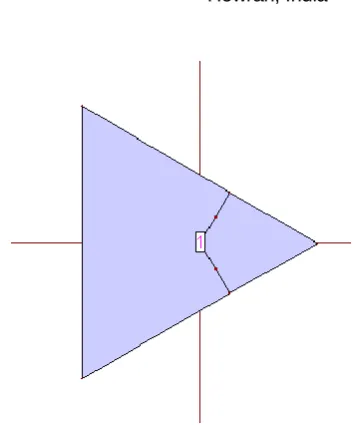
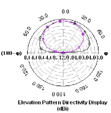
[image:1.595.338.516.175.388.2]Basic parameters of ETMSA are εr=3.2; h=1.6 mm,tanδ =0.001 and length of each arm of ETMSA =20 mm is taken. The co-axial feed is at (0,0),Which shows the resonant frequency of 5.249GHz as shown in fig.1a and fig.1b.The percentage bandwidth is equal to 1% for -10dB return loss. The corresponding directive gain is shown infig.1c. The gain value is 6.806dbi (approx.).Simulation has been done by the method of moment based IE3D EM Design System (V: 14) simulator [8].
Figure 1a: IE3D Simulated View patch without pin shorting.
[image:1.595.320.568.442.611.2]Figure 1c: Radiation pattern at f=5.249 GHz
2.1 EFFECT OF SINGLE PIN SHORTING
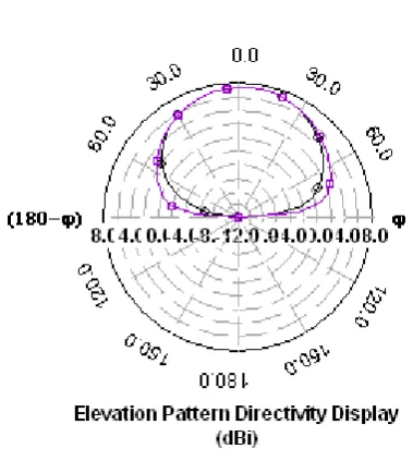
[image:2.595.336.524.106.310.2]When Pin(P1) is shorted between vertex and co-axial feed point as shown in fig.2a.the resonant frequency shifted from 5.249GHz to 6.9GHz as shown in fig.2b.In proposed antenna the position of P1 from vertex is 1.65mm.The corresponding directive gain is 7.824dbi as shown in fig.2cAlso, the impedance bandwidth becomes higher (7.2%), as shown in table (1).
Figure 2a: Effect of single Pin shorting.
Figure 2b: Return Loss Performance for single pin shorting.
Figure 2c: Radiation pattern at f=6.9 GHz
Table: 1
Pin effect fc (GHz) Return loss (dB)
% B.W. (GHz)
Without Pin 5.25 -16.17 1
With single Pin P1
6.9 -20.67 7.2
2.2 EFFECT OF TWO PIN SHORTING
[image:2.595.90.248.427.560.2] [image:2.595.56.290.592.734.2]Figure 3a: Effect of dual Pin shorting.
Figure 3b: Return Loss Performance for two pin shorting.
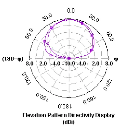
Figure3.c: Radiation pattern at f1=6.03 GHz. (For two pin
shorting).
Figure3.d: Radiation pattern at f2=7.238 GHz. (For two
pin shorting).
Table: 2
Circular polarization
f1(GHz)
% B.W(GHz)
f2(GHz)
% B.W.(GHz)
LHCP 6.03 2.8 7.238 5.3
RHCP 5.98 2.85 7.2 5.32
2.3 EFFECT OF TWO PIN SHORTING
WITH A CIRCULAR NOTCH
[image:3.595.71.261.523.735.2]Figure 4a: Effect of two Pin shorting with a circular notch.
Figure 4b: Return Loss Performance for two pin shorting with a circular notch.
Figure4.c: Radiation pattern at f1=6.631 GHz. (For two
pin shorting with a circular notch).
Figure4.d: Radiation pattern at f2=7.1398 GHz. (For two
pin shorting with a circular notch).
Figure4.e: Radiation pattern at fc=6.98 GHz. (For two pin
shorting with a circular notch).
Table: 3
f1(GHz) f2(GHz) fc(GHz)
% B.W.(GHz)
Return loss for f1 (dB)
Return loss for f2 (dB)
[image:4.595.71.264.532.737.2]1.1 1.2 1.3 1.4 1.5 1.6 0 1 2 3 4 5 6 7 8 9 10 11 12 13 % B. W . (G H z) h (mm) r=2.6 r=3.2
r=4.4
r=6.4
Figure5.a:%B.W vs. thickness plot for different value of dielectric constant.
2 3 4 5 6 7
0 2 4 6 8 10 12 14 16 % B. W . r h=1.6 m.m h=1.5 m.m h=1.3 m.m h=1.1 m.m
Figure5.b:%B.W vs. relative permittivity plot for different value of substrate thickness.
4.
DIRECTIVITY
For the proposed antenna the sufficient directivity (in dBi) can be achieved in between the utilized bandwidth from 6GHz to 8.5GHz with maximum directivity of 7.85dBi at 7.4GHz as shown in fig.6.
antenna with circular notch.
5.
CONCLUSION
The simulation carried out on the new proposed antenna. The two pin shorting effect produces dual band and the notch loading along with the two shorting pins results in enhanced bandwidth performance. Bandwidth performance of this antenna is also examined for various antenna parameters such as substrate thickness and substrate permittivity. It is concluded that for higher value of permittivity the percentage bandwidth significantly decreases with increasing thickness.
6.
REFERENCES
[1] Pozar, D. M. and D. H. Schaubert, Microstrip Antennas: The Analysis and Design of Microstrip Antennas and Arrays, IEEE Press, New York, 1995.
[2] Zhang, Y. P.and J. J. Wang,\Theory and analysis of di®erentially-drivenmicrostrip antennas," IEEE Trans. Antennas Propag., Vol. 54, 1092{1099, 2006.
[3] S. Sadat, M. Fardis, F. Geran, G. Dadashzadeh, N. Hojjat and M. Roshandel, “A Compact Microstrip Square-Ring Slot Antenna for UWB Applications,” IEEE Antennas and propagation Society International Symposium, 9-14 July 2006, pp. 4629-4632.
[4] K. F. Lee, K. M. Luk, K. F. Tong, S. M. Shum, T. Huynk and R. Q. Lee, “Experimental and Simulation Studies of the Coaxially Fed U-slot Rectangular Patch” IEEE Proceedings of Microwave Antenna Propagation, Vol. 144, No. 5, October 1997, pp. 354-358.
[5] Deshmukhet. al., “Multiband Configurations of stub- Loaded slotted Rectangular Microstrip Antenna”, IEEE Antennas and Propagation Magazine, Vol. 52, No.1 2010.
[6] Y. J. Sung M. Kim, and Y.-S. Kim, “Harmonics Reduction With Defected Ground Structure for a Microstrip Patch Antenna”, IEEE Antennas and Wireless Propagation Letters,VOL. 2, 2003.
[7] Matin, M. M., B. S. Sharif, and C. C. Tsimenidis, \Probe fed stacked patch antenna for wideband applications," IEEE Trans. Antennas Propag., Vol. 55, No. 8, 2385{2388, 2007.5. Wi, S. H., Y. B. Sun, I. S. Song, S. H. Choa, I. S. Koh, Y. S. Lee, and J. G. Yook, \Package-Level integrated antennas based onLTCC technology," IEEE Trans. Antennas Propag., Vol. 54, No. 8,2190{2197, 2006.