Technology (IJRASET)
Efficient Fixed-Point DLMS Adaptive Filter
Implementation on FPGA
J.Shobha1, Y.Murali, M.Tech2
Department of Electronics and communication Engineering Audisankara College of Engineering & Technology, Gudur, (Autonomous)
Abstract- In this paper, we present an efficient architecture for the implementation of a delayed least mean square adaptive filter. For achieving lower adaptation-delay and area-delay-power efficient implementation, we use a novel partial product generator and propose a strategy for optimized balanced pipelining across the time-consuming combinational blocks of the structure. From synthesis results, we find that the proposed design offers nearly 17% less area-delay product (ADP) and nearly 14% less energy-delay product (EDP) than the best of the existing systolic structures, on average, for filter lengths N = 8, 16, and 32. We propose an efficient fixed-point implementation scheme of the proposed architecture, and derive the expression for steady-state error. We show that the steady-state mean squared error obtained from the analytical result matches with the simulation result. Moreover, we have proposed a bit-level pruning of the proposed architecture, which provides nearly 20% saving in ADP and 9% saving in EDP over the proposed structure before pruning without noticeable degradation of steady-state-error performance.
Index Terms—Adaptive filters, circuit optimization, fixed-point arithmetic, least mean square (LMS) algorithms.
I. INTRODUCTION
THE LEAST MEAN SQUARE (LMS) adaptive filter is the most popular and most widely used adaptive filter, not only because of its simplicity but also because of its satisfactory convergence performance [1], [2]. The direct-form LMS adaptive filter involves a long critical path due to an inner-product computation to obtain the filter output. The critical path is required to be reduced by pipelined implementation when it exceeds the desired sample period. Since the conventional LMS algorithm does not support pipelined implementation because of its recursive behavior, it is modified to a form called the delayed LMS (DLMS) algorithm [3]– [5], which allows pipelined implementation of the filter.
A lot of work has been done to implement the DLMS algorithm in systolic architectures to increase the maximum usable frequency [3], [6], [7] but, they involve an adaptation delay of ~N cycles for filter length N, which is quite high for large order filters. Since the convergence performance degrades considerably for a large adaptation delay, Visvanathan et al. [8] have proposed a modified systolic architecture to reduce the adaptation delay. A transpose-form LMS adaptive filter is suggested in [9], where the filter output at any instant depends on the delayed versions of weights and the number of delays in weights varies from 1 to N. Van and Feng [10] have proposed a systolic architecture, where they have used relatively large processing elements (PEs) for achieving a lower adaptation delay with the critical path of one MAC operation.
Ting et al. [11] have proposed a fine-grained pipelined design to limit the critical path to the maximum of one addition time, which supports high sampling frequency, but involves a lot of area overhead for pipelining and higher power consumption than in [10], due to its large number of pipeline latches.
Further effort has been made by Meher and Maheshwari [12] to reduce the number of adaptation delays. Meher and Park have proposed a 2-bit multiplication cell, and used that with an efficient adder tree for pipelined inner-product computation to
minimize the critical path and silicon area without increasing the number of adaptation delays [13], [14].
The existing work on the DLMS adaptive filter does not discuss the fixed-point implementation issues, e.g., location of radix point, choice of word length, and quantization at various stages of computation, although they directly affect the convergence performance, particularly due to the recursive behavior of the LMS algorithm. Therefore, fixed-point implementation issues are given adequate emphasis in this paper. Besides, we present here the optimization of our previously reported design [13], [14] to reduce the number of pipeline delays along with the area, sampling period, and energy consumption. The proposed design is found to be more efficient in terms of the power- delay product (PDP) and energy-delay product (EDP) compared to the existing structures.
Technology (IJRASET)
implementation. Section IV deals with fixed-point implementation considerations and simulation studies of the convergence of the algorithm. In Section V, we discuss the synthesis of the proposed architecture and comparison with the existing architectures. Conclusions are given in Section VI.
II. REVIEW OF DELAYED LMS ALGORITHM
The weights of LMS adaptive filter during the nth iteration are updated according to the following equations [2]: = + . . 1( )
Where
= − , = . 1( )
where the input vector xn, and the weight vector wnat the nth iteration are, respectively, given by
xn= [xn, xn−1, . . . , xn−N+1]T wn= [wn(0),wn(1), . . . ,wn(N − 1)]T,
dnis the desired response, ynis the filter output, and endenotes the error computed during the nth iteration. μ is thestep-size, and N is the number of weights used in the LMSadaptive filter.
In the case of pipelined designs with m pipeline stages, the error en becomes available after m cycles, where m is called the “adaptation delay.” The DLMS algorithm therefore uses the delayed error en−m, i.e., the error corresponding to (n −m)th iteration for updating the current weight instead of the recent-most error. The weight-update equation of DLMS adaptive filter is given by
= + . . (2)
The block diagram of the DLMS adaptive filter is shown in Fig. 1, where the adaptation delay of m cycles amounts to the delay introduced by the whole of adaptive filter structure consisting of finite impulse response (FIR) filtering and the weight- update process.
Fig.1 Structure of the conventional delayed LMS adaptive filter.
It is shown in [12] that the adaptation delay of conventional LMS can be decomposed into two parts: one part is the delay introduced by the pipeline stages in FIR filtering, and the other part is due to the delay involved in pipelining the weight update process. Based on such a decomposition of delay, the DLMS adaptive filter can be implemented by a structure shown in Fig. 2.
Fig.2 Structure of the modified delayed LMS adaptive filter.
Technology (IJRASET)
used with the input samples delayed by n1 cycles to generate the weight-increment term. The weight- update equation of the modified DLMS algorithm is given by
= + . . (3 ) Where
= − , (3 )
= . 3( )
We notice that, during the weight update, the error with n1 delays is used, while the filtering unit uses the weights delayed by n2 cycles. The modified DLMS algorithm decouples computations of the error-computation block and the weight-update block and allows us to perform optimal pipelining by feed forward cut-set retiming of both these sections separately to minimize the number of pipeline stages and adaptation delay.
The adaptive filters with different n1 and n2 are simulated for a system identification problem. The 10-tap band-pass filter with impulse response is
ℎ =sin( ( −4.5)) ( −4.5) −
sin( ( −4.5)) ( −4.5) For n=0,1,2,….,9 otherwise hn=0 (4)
used as the unknown system as in [10]. wHand wLrepresent the high and low cutoff frequencies of the pass band, and are set to wH= 0.7π and wL= 0.3π, respectively. Thestep size μ is set to 0.4. A 16-tap adaptive filter identifiesthe unknown system with Gaussian random input xn of zeromean and unit variance. In all cases, outputs of known systemare of unity power, and contaminated with white Gaussiannoise of −70 dB strength.
III. PROPOSED ARCHITECTURE
As shown in Fig. 2, there are two main computing blocks in the adaptive filter architecture: 1) the error-computation block, and 2) weight-update block. In this Section, we discuss the design strategy of the proposed structure to minimize the adaptation delay in the error-computation block, followed by the weight-update block.
A. Pipelined Structure of the Error-Computation Block
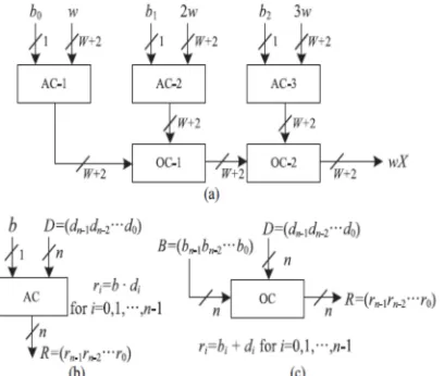
[image:4.612.202.410.463.672.2]The proposed structure for error-computation unit of an N-tap DLMS adaptive filter is shown in Fig. 3.
Fig. 3 Proposed structure of the error-computation block.
It consists of N number of 2-b partial product generators (PPG) correspondingto N multipliers and a cluster of L/2 binary adder trees,followed by a single shift–add tree. Each sub-block is describedin detail.
Technology (IJRASET)
number of AND/OR cells (AOC).1 Each of the 2-to-3 decoders takes a 2-b digit (u1u0) as input and produces three outputs b0 = u0 · . u1, b1 = . u0 · u1, and b2 = u0 · u1, such that b0 = 1 for (u1u0) = 1, b1 = 1 for (u1u0) = 2, and b2 = 1 for (u1u0) = 3. The decoder output b0, b1 and b2 along with w, 2w, and 3w are fed to an AOC, where w, 2w, and 3w are in 2’s complement representation and sign-extended to have (W + 2) bits each.
[image:5.612.206.410.179.371.2]To take care of the sign of the input samples while computing the partial product corresponding to the most significant digit (MSD), i.e., (uL−1uL−2) of the input sample, the AOC (L/2 − 1) is fed with w, −2w, and −w as input since (u L−1 u L−2) can have four possible values 0, 1, −2, and −1.
Fig. 4 Proposed structure of PPG. AOC stands for AND/OR cell.
2) Structure of AOCs: The structure and function of an AOC are depicted in Fig. 5. Each AOC consists of three AND cells and two OR cells. The structure and function of AND cells and OR cells are depicted by Fig. 5(b) and (c), respectively. Each AND cell takes an n-bit input D and a single bit input b, and consists of n AND gates. It distributes all the n bits of input D to its n
AND gates as one of the inputs. The other inputs of all the n AND gates are fed with the single-bit input b. As shown in Fig. 5(c), each OR cell similarly takes a pair of n-bit input words and has n OR gates. A pair of bits in the same bit position in B and
D is fed to the same OR gate. The output of an AOC is w, 2w, and 3w corresponding to the decimal values 1, 2, and 3 of the 2-b input (u1u0), respectively.
Fig.5.Structure and function of AND/OR cell. Binary operators · and + in (b) and (c) are implemented using AND and OR gates, respectively.
[image:5.612.210.414.488.661.2]Technology (IJRASET)
performs L/2 parallel multiplications of input word w with a 2-b digit to produce L/2 partial products of the product word wu.
3) Structure of Adder Tree
Conventionally, we should have performed the shift-add operation on the partial products of each PPG separately to obtain the product value and then added all the N product values to compute the desired inner product. However, the shift-add operation to obtain the product value increases the word length, and consequently increases the adder size of N − 1 additions of the product values. To avoid such increase in word size of the adders, we add all the N partial products of the same place value from all the N
PPGs by one adder tree.
All the L/2 partial products generated by each of the N PPGs are thus added by (L/2) binary adder trees. The outputsof the L/2 adder trees are then added by a shift-add treeaccording to their place values. Each of the binary adder treesrequire log2 N stages of adders to add N partial product, andthe shift–add tree requires log2 L − 1 stages of adders to add L/2 output of L/2 binary adder trees.2 The addition schemefor the error-computation block for a four-tap filter and inputword size L = 8 is shown in Fig. 6.
Fig.6. Adder-structure of the filtering unit for N = 4 and L = 8.
For N = 4 and L = 8, theadder network requires four binary adder trees of two stageseach and a two-stage shift–add tree. In this figure, we haveshown all possible locations of pipeline latches by dashed lines, to reduce the critical path to one addition time. If we introduce pipeline latches after every addition, it would require L(N − 1)/2 + L/2 − 1 latches in log2N + log2L − 1 stages, which would lead to a high adaptation delay and introduce a large overhead of area and power consumption for large values of N and L. On the other hand, some of those pipeline latches are redundant in the sense that they are not required to maintain a critical path of one addition time. The final adder in the shift–add tree contributes to the maximum delay to the critical path. Based on that observation, we have identified the pipeline latches that do not contribute significantly to the critical path and could exclude those without any noticeable increase of the critical path.
B. Pipelined Structure of the Weight-Update Block
Technology (IJRASET)
Fig.7.Proposed structure of the weight-update block.
Each of the MAC units therefore performs the multiplication of the shifted value of error with the delayed input samples xi followed by the additions with the corresponding old weight values wi. All the N multiplications for the MAC operations are performed by N PPGs, followed by N shift– add trees. Each of the PPGs generates L/2 partial products corresponding to the product of the recently shifted error value μ × e with L/2, the number of 2-b digits of the input word xi , where the sub-expression 3μ×e is shared within the multiplier. Since the scaled error (μ×e) is multiplied with all the N delayed input values in the weight-update block, this sub-expression can be shared across all the multipliers as well.
This leads to substantial reduction of the adder complexity. The final outputs of MAC units constitute the desired updated weights to be used as inputs to the error-computation block as well as the weight-update block for the next iteration.
C. Adaptation Delay
As shown in Fig. 2, the adaptation delay is decomposed into n1 and n2. The error-computation block generates the delayed error by
n1−1 cycles as shown in Fig. 3, which is fed to the weight-update block shown in Fig. 8 after scaling by μ; then the input is delayed by 1 cycle before the PPG to make the total delay introduced by FIR filtering be n1. In Fig. 7, the weight-update block generates wn−1−n2, and the weights are delayed by n2+1 cycle. However, it should be noted that the delay by 1 cycle is due to the latch before the PPG, which is included in the delay of the error-computation block, i.e., n1. Therefore, the delay generated in the weight-update block becomes n2. If the locations of pipeline latches are decided, n1 becomes 5, where three latches are in the error-computation block, one latch is after the subtraction in Fig. 3, and the other latch is before PPG in Fig. 7. Also, n2 is set to 1 from a latch in the shift-add tree in the weight-update block.
D. Adder-Tree Optimization
Technology (IJRASET)
Fig.8. Dot-diagram for optimization of the adder tree in the case of N = 4, L = 8, and W = 8.
Each row of the dot diagram contains 10 dots, which represent the partial products generated by the PPG unit, for W = 8. We have four sets of partial products corresponding to four partial products of each multiplier, since L = 8. Each set of partial products of the same weight values contains four terms, since N = 4. The final sum without truncation should be 18 b. However, we use only 8 b in the final sum, and the rest 10 b are finally discarded.
To reduce the computational complexity, some of the LSBs of inputs of the adder tree can be truncated, while some guard bits can be used to minimize the impact of truncation on the error performance of the adaptive filter. In Fig.8, four bits
are taken as the guard bits and the rest six LSBs are truncated.To have more hardware saving, the bits to be truncated are not generated by the PPGs, so the complexity of PPGs also gets reduced.
IV. SIMULATION RESULTS
The simulations of the proposed LMS adaptive filter structure are carried out by using Verilog HDL in Xilinx tool. The RTL schematic and simulation results of proposed LMS adaptive filter are shown in below figures.
Fig.9 RTL schematic of proposed design Truncated
bits
Guard bits
Technology (IJRASET)
Fig.10 simulation results of proposed design
V. CONCLUSION
We proposed an area–delay-power efficient low adaptation delay architecture for fixed-point implementation of LMS adaptive filter. We used a novel PPG for efficient implementation of general multiplications and inner-product computation by common sub-expression sharing. Besides, we have proposed an efficient addition scheme for inner-product computation to reduce the adaptation delay significantly in order to achieve faster convergence performance and to reduce the critical path to support high input-sampling rates. Aside from this, we proposed a strategy for optimized balanced pipelining
across the time-consuming blocks of the structure to reduce the adaptation delay and power consumption, as well. The proposed structure involved significantly less adaptation delay and provided significant saving of ADP and EDP compared to the existing structures.
REFERENCES
[1] B. Widrow and S. D. Stearns, Adaptive Signal Processing. Englewood Cliffs, NJ, USA: Prentice-Hall, 1985. [2] S. Haykin and B. Widrow, Least-Mean-Square Adaptive Filters. Hoboken, NJ, USA: Wiley, 2003.
[3] M. D. Meyer and D. P. Agrawal, “A modular pipelined implementation of a delayed LMS transversal adaptive filter,” in Proc. IEEE Int. Symp. Circuits Syst., May 1990, pp. 1943–1946.
[4] G. Long, F. Ling, and J. G. Proakis, “The LMS algorithm with delayed coefficient adaptation,” IEEE Trans. Acoust., Speech, Signal Process., vol. 37, no. 9, pp. 1397–1405, Sep. 1989.
[5] G. Long, F. Ling, and J. G. Proakis, “Corrections to ‘The LMS algorithm with delayed coefficient adaptation’,” IEEE Trans. Signal Process., vol. 40, no. 1, pp. 230–232, Jan. 1992.
[6] H. Herzberg and R. Haimi-Cohen, “A systolic array realization of an LMS adaptive filter and the effects of delayed adaptation,” IEEE Trans. Signal Process., vol. 40, no. 11, pp. 2799–2803, Nov. 1992.
[7] M. D. Meyer and D. P. Agrawal, “A high sampling rate delayed LMS filter architecture,” IEEE Trans. Circuits Syst. II, Analog Digital Signal Process., vol. 40, no. 11, pp. 727–729, Nov. 1993.
[8] S. Ramanathan and V. Visvanathan, “A systolic architecture for LMS adaptive filtering with minimal adaptation delay,” in Proc. Int. Conf. Very Large Scale Integr. (VLSI) Design, Jan. 1996, pp. 286–289.
[9] Y. Yi, R. Woods, L.-K. Ting, and C. F. N. Cowan, “High speed FPGA-based implementations of delayed-LMS filters,” J. Very Large Scale Integr. (VLSI) Signal Process., vol. 39, nos. 1–2, pp. 113–131, Jan. 2005.
[10] L. D. Van and W. S. Feng, “An efficient systolic architecture for the DLMS adaptive filter and its applications,” IEEE Trans. Circuits Syst. II, Analog Digital Signal Process., vol. 48, no. 4, pp. 359–366,
Apr. 2001.
[11] L.-K. Ting, R. Woods, and C. F. N. Cowan, “Virtex FPGA implementation of a pipelined adaptive LMS predictor for electronic support measures receivers,” IEEE Trans. Very Large Scale Integr. (VLSI) Syst., vol. 13, no. 1, pp. 86–99, Jan. 2005.
[12] P. K. Meher and M. Maheshwari, “A high-speed FIR adaptive filter architecture using a modified delayed LMS algorithm,” in Proc. IEEE Int. Symp. Circuits Syst., May 2011, pp. 121–124.
[13] P. K. Meher and S. Y. Park, “Low adaptation-delay LMS adaptive filter part-I: Introducing a novel multiplication cell,” in Proc. IEEE Int. Midwest Symp. Circuits Syst., Aug. 2011, pp. 1–4.
Technology (IJRASET)
Aug. 2011, pp. 1–4.
[15] K. K. Parhi, VLSI Digital Signal Procesing Systems: Design and Implementation. New York, USA: Wiley, 1999.
[16] C. Caraiscos and B. Liu, “A roundoff error analysis of the LMS adaptive algorithm,” IEEE Trans. Acoust., Speech, Signal Process., vol. 32, no. 1, pp. 34–41, Feb. 1984.
[17] R. Rocher, D. Menard, O. Sentieys, and P. Scalart, “Accuracy evaluation of fixed-point LMS algorithm,” in Proc. IEEE Int. Conf. Acoust., Speech, Signal Process., May 2004, pp. 237–240.
AUTHOR’S PROFILE
Jadapalli Shobha received her B.Tech degree in Electronics and communication Engineering from Geethanjali institute of science and technology, Gangavaram(vi), kovur mandal, Nellore District, affiliated to JNTU Anantapur. She is currently pursuing M.Tech VLSI in Audisankara college of Engineering and Technology, Gudur(Autonomous), SPSR Nellore (Dist), affiliated to JNTU Anantapur.