Deposition and characterisation of (Ti,Zr) based hard
compound and multi-layer PVD films.
DOHUE, Lee Adrian.
Available from Sheffield Hallam University Research Archive (SHURA) at:
http://shura.shu.ac.uk/19570/
This document is the author deposited version. You are advised to consult the publisher's version if you wish to cite from it.
Published version
DOHUE, Lee Adrian. (1995). Deposition and characterisation of (Ti,Zr) based hard compound and multi-layer PVD films. Doctoral, Sheffield Hallam University (United Kingdom)..
Copyright and re-use policy
See http://shura.shu.ac.uk/information.html
ProQuest Number: 10694451
All rights reserved
INFORMATION TO ALL USERS
The quality of this reproduction is dependent upon the quality of the copy submitted.
In the unlikely event that the author did not send a com plete manuscript and there are missing pages, these will be noted. Also, if material had to be removed,
a note will indicate the deletion.
uest
ProQuest 10694451
Published by ProQuest LLC(2017). Copyright of the Dissertation is held by the Author.
All rights reserved.
This work is protected against unauthorized copying under Title 17, United States C ode Microform Edition © ProQuest LLC.
ProQuest LLC.
789 East Eisenhower Parkway P.O. Box 1346
DEPOSITION AND CHARACTERISATION
OF (Ti,Zr) BASED HARD COMPOUND AND
MULTI-LAYER PVD FILMS.
Lee Adrian Donohue.
A thesis submitted in partial fulfilment of the
requirements of
Sheffield Hallam University
for the degree of Doctor of Philosophy.
November 1995.
ABSTRACT.
Industrial recognition of the importance of optimising engineering component performance has recently led to a significant increase in the use of surface coating technologies. An important process for the production of such coatings is Physical Vapour Deposition (PVD) which has proved to be a consistent, reliable and improving technique for industry. In the area of advanced wear resistant coatings however, fundamental research to improve deposition efficiency and enhance coating performance has been required. This thesis describes research investigating the following three
areas:-A series of experiments was carried out to study the design, metallurgy and performance of TiZr, ZrMo and TiMo segmented targets for use in steered cathodic arc evaporation and unbalanced magnetron sputter PVD techniques. A hot isostatic pressing technique was used to manufacture a range of prototype targets by diffusion bonding of appropriate metallic segments to controllable depths. In steered arc evaporation trials, a deleterious evaporation phenomenon occurred at segment interfaces when the cathode spot traversed from high vapour pressure to low vapour pressure materials. Analysis of the spot motion has led to the proposal of a simple model. Reactive unbalanced magnetron sputtering trials successfully produced a range of TiZrN, TiMoN and ZrMoN coatings of compositions in good agreement with Monte-Carlo simulation predictions. However, preferential poisoning of the high reactivity metal segments on TiMo and ZrMo targets was found to occur during high N2
partial pressure processes. A comparative study of unbalanced magnetron sputtering, steered arc evaporation and the hybrid arc-bond sputter technique has been made during deposition trials on the ternary TiZrN hard coating system. Examination of the influence of two process parameters, substrate bias voltage and nitrogen partial pressure, on the mechanical and physical properties of TiZrN coatings is also reported. Stoichiometric TiZrN films were generally found to exhibit a <1 1 1> single phase, face centred cubic structure with lattice
parameters which followed Vegard's law. Alteration of the elemental composition of the alloy could be achieved by altering the power to individual magnetron cathodes or varying the current of the arc discharge during co-deposition. Solid solution strengthening mechanisms produced high hardness values (25OO-36OOH0 which maximised as the alloy composition approached TiQ ^Zrq^. Further studies have been undertaken where A1 was partially
substituted for Zr within the lattice to enhance oxidation resistance properties and a range of fully adherent TiAlZrN quaternary films on high speed steel substrates were produced. The development of an original technique for industrial scale fabrication of a range of hard, low period (<150A) multi-layer PVD thin films is outlined and the effects of substrate rotation velocity, type of rotation (1-fold or 3-fold) and deposition rate have been investigated. The high level of lattice mis-match and substantial differences in dislocation line energy and shear modulus has given rise to TiAlN-ZrN films exhibiting Knoop micro-hardness in excess of 4000Hk. Bulk and micro-analysis techniques have indicated a reproducible lamella coating structure can be formed, with accurate control of the layer period. Excellent levels of coating adhesion were implemented by a metal ion etch substrate pre-treatment and the deposition of a sputtered base layer and films exhibited relatively low surface roughness and high density. A coating strategy, based upon the reactivity of the individual target materials and the
characteristics of arc evaporated and magnetron sputtered vapour fluxes, has been determined which provides high flexibility in the coating elemental composition. The investigations clearly indicate that the multi-layer coating methods utilised allow the deposition of 3rd generation films without a productivity loss in comparison to 1st generation and 2nd
ADVANCED STUDIES.
As part of the course of study I attended the following conferences and workshops combined with a number of informal research seminars presented at Sheffield Hallam University by academic staff from the Materials Research Institute and the Division of Applied Physics.
• "3rd International Conference on Advances in Coatings and Surface Engineering for Corrosion and Wear Resistance", May 1992, Newcastle Polytechnic.
• "Hard Coatings by PVD Methods and Evaluation Techniques Workshop", October 1992, Sheffield Hallam University.
• "21st International Conference on Metallurgical Coatings and Thin Films", April 1993, San Diego, California, United States of America.
• "International Conference on Advanced Materials and Processing Technologies",
August 1993, Dublin City University, Dublin, Eire.
• "22ndInternational Conference on Metallurgical Coatings and Thin Films", April 1994, San Diego, California, United States of America.
• "4{h International Conference on Plasma Surface Engineering", October 1994, Garmisch-Partenkirchen, Germany,
• "3rd European Workshop on Plasma Surface Engineering", June 1995, Wurzburg, Germany.
• "International Conference on Advanced Materials and Processing Technologies",
PUBLICATIONS.
"Design and performance o f a hot isostatically pressed Ti-Zr segmented cathode for electromagnetically steered arc physical vapour deposition".
L.A.Donohue, J.Cawley, J.S.Brooks - Surface and Coating Technology, 63,1994,49- 56. Presented at ICMCTF-93, San Diego, California, USA, April 1993 and The Iron and Steel Institute of Japan, Tokyo, 1993.
"Fabrication and Performance o f novel segmented cathodes for arc evaporative and magnetron sputter physical vapour deposition".
J.Cawley, L.A.Donohue, J.S.Brooks - Presented at AMPT-93, Dublin, Eire, August 1993.
"Design and assessment o f segmented targets in PVD".
L.A.Donohue, J.Cawley, J.S.Brooks - Poster presented at EAST conference, Schwabisch Gmund, F.R.G, 1993.
"Deposition and characterisation o f Arc-Bond Sputter TiZrN coatings from pure metallic and segmented targets".
L.A.Donohue, J.Cawley, J.S.Brooks - Surface and Coating Technology, 72,1995,128- 138. Presented at ICMCTF-94, San Diego, California, USA, April 1994.
"Deposition and characterisation ofTiAlZrN films produced by a combined steered arc and unbalanced magnetron sputtering technique ".
L.A.Donohue, J.Cawley, J.S.Brooks, W-D.Miinz - Surface and Coating Technology, 74- 75, 1995,123. Presented at Plasma Surface Engineering-94, Garmisch-Partenkirchen, F.R.G, 1994 and the satellite meeting of LCS-94, Ehime University, Matsuyama, Japan,
1994.
"Investigation o f superlattice coatings deposited by a combined steered arc evaporation and unbalanced magnetron sputtering technique".
"Large scale fabrication o f hard superlattice thin films by combined steered arc evaporation and unbalanced magnetron sputtering".
L.A.Donohue, W-D.Miinz, J.Cawley, T.Hurkmans, T.Trinh, I.Petrov, J.E.Greene - Presented at 3rd European Workshop on Plasma Surface Engineering, Wurzburg, Germany, June 1995. In press Surface and Coatings Technology.
"Characterisation ofTiAlN-ZrN superlattice thin films produced by variable PVD deposition regimes".
ACKNOWLEDGEMENTS.
The author would like to sincerely thank the following people and collaborating establishments for their helpful discussions and advice during the period of study:
• Dr J.Cawley, Professor J.S.Brooks, Professor W-D.Miinz & the staff of the Materials Research Institute, Sheffield Hallam University, United Kingdom.
• T.Hurkmans & T.Trinh - Hauzer Techno Coating Europe B.V, Venlo, Netherlands.
• Dr H.Jehn, Dr B.Rother, H.Kappl & staff - Forschungsinstitut fur Edelmetalle und Metallchemie, Schwabisch-Gmund, F.R.G.
• Deutscher Akademischer Austauschdienst (DAAD), Bonn, F.R.G.
• Professor Allan Matthews & staff - Research Centre for Surface Engineering, Hull University, United Kingdom.
• Dr Sue King - H.I.P. Infutec Ltd, Chesterfield, United Kingdom
• Atomic Energy Authority, Harwell, Oxford, United Kingdom.
• The Department of Metallurgy, University of Sheffield, United Kingdom.
• Dr Ivan Petrov - University of Illinois at Urbana-Champaign, Urbana, USA.
• IBM Research, Yorktown Heights, New York, USA.
• Dr M.Ives, Dr C.Blomfield (The lads at 157), Dr P.Walke and the rest of the MRI and Physics research students - For the laughter and entertainment they have provided throughout the years.
• Higher Education Funding Council England (HEFCE) for funding this project.
CONTENTS
Chapter One: Introduction...1
1.1. Surface engineering.
1.2. Physical vapour deposition (PVD). 1.3. PVD hard coating developments. 1.4. Present work.
Chapter Two: Literature Review... 9
2.1. Sputtering techniques.
2.1.1. Sputtering processes and energetic particle interactions. 2.1.2. D.C. diode sputtering - the self-sustained glow discharge. 2.1.3. Glow discharge characteristics.
2.1.4. D.C. triode sputtering
2.1.5. Magnetron enhanced sputtering. 2.1.6. The unbalanced magnetron.
2.1.7. Multi-cathode systems and closed field geometry. 2.1.8. Reactive sputtering.
2.2. Arc evaporation techniques. 2.2.1. The random cathodic arc. 2.2.2. The cathode spot life cycle. 2.2.3. The types of cathode spot.
2.2.4. The spot diameter and current density. 2.2.5. Spot splitting.
2.2.6. The types of erosion 2.2.7. The random spot motion. 2.2.8. The steered arc.
2.2.9. The filtered arc.
2.2.10. Arc evaporation of multi-elemental targets.
2.4. Film deposition.
2.4.1. Nucleation and growth mechanisms.
2.4.2. Structure zone models and film microstructure. 2.4.3. Ar+sputter etching and metallic interlayers. 2.4.4. Bias edge effects.
2.4.5. Residual stress.
2.5. Coating Systems.
2.5.1. First generation of PVD hard coatings. 2.5.2. Second generation of PVD hard coatings. 2.5.3. Third generation of PVD hard coatings.
2.6. Summary.
Chapter Three: Experimental... 67
3.1. Physical vapour deposition equipment.
3.1.1. The electromagnetic steered arc evaporation PVD unit. 3.1.2. The unbalanced magnetron sputter PVD unit.
3.1.3. The arc-bond sputter PVD unit.
3.2. Target manufacturing technique.
3.3. Sample preparation for coating.
3.4. Sample preparation techniques for analysis.
3.4.1. Scanning electron microscopy fracture cross-sections. 3.4.2. Transmission electron microscope coating cross-sections.
3.5. Characterisation techniques. 3.5.1. X-ray diffraction.
3.5.2. Scanning electron microscopy. 3.5.3. Transmission electron microscopy.
3.5.4. Glow discharge optical emission spectroscopy (GDOES). 3.5.5. Vickers hardness test.
3.5.8. Scratch adhesion testing.
3.5.9. Rockwell indentation adhesion testing. 3.5.10. Colourimetry.
3.5.11. Surface roughness profiling.
3.6. Summary of equipment and techniques.
Chapter Four: Investigation of TiZr, TiMo & ZrMo segmented targets...104
4.1. TiZr Model alloy investigations.
4.1.1. Alloy manufacture, preparation and equilibrium studies. 4.1.2. Results of 20%Ti / 80%Zr alloy investigations.
4.1.3. Results of 50%Ti / 50%Zr alloy investigations. 4.1.4. Results of 80%Ti / 20%Zr alloy investigations.
4.2. Mechanical and physical properties of TiZr, TiMo and ZrMo segmeted targets.
4.2.1. X-ray diffraction results. 4.2.2. Microstructural analysis. 4.2.3. Interfacial microscopy.
4.2.4. Interfacial diffusion analysis by X-ray line-scanning. 4.2.5. Hardness measurements.
4.3. Segmented target performance in steered arc evaporation trials. 4.3.1. TiZr target performance.
4.3.2. TiMo target performance. 4.3.3. ZrMo target performance.
4.4. Simulation of segmented target sputter and ion etching performance. 4.4.1. Sputter yields and ion ranges.
4.4.2. Simulation of substrate ion etching. 4.4.3. Simulation of substrate sputter coating. 4.4.4. Simulation of substrate arc coating.
4.5.2. Mechanical and physical properties of TiMoN and ZrMoN ternary coatings.
4.5.3. Flux distribution analysis
Chapter Five: Investigation of the TiZrN system... 147
5.1. Examination of TixZryN coatings deposited by SCAE, UBM and ABS techniques.
5.1.1. X-ray diffraction results. 5.1.2. GDOES results.
5.1.3. Scanning electron microscopy results. 5.1.4. Mechanical and physical properties.
5.2. Parameter study.
5.2.1. X-ray diffraction results. 5.2.2. GDOES results.
5.2.3. Scanning electron microscopy results. 5.2.4. Mechanical and physical properties.
5.3. Investigation of the TiAlZrN system. 5.3.1. Experimental conditions. 5.3.2. X-ray diffraction results. 5.3.3. GDOES results.
5.3.4. Scanning electron micrscopy results. 5.3.5. Mechanical and physical properties.
Chapter Six: Growth and characterisation of TiAlN-ZrN and TiAIN-TiN multi-layer thin films...197
6.1. Multi-layer process conditions.
6.2. The effect of rotation velocity and type of rotation on TiAlN-ZrN multi-layer films.
6.2.1. X-ray diffraction results. 6.2.2. GDOES results.
6.2.5. Knoop micro-hardness results. 6.2.6. Surface roughness results. 6.2.7. Thickness and deposition rate.
6.2.8. Rockwell and scratch adhesion results. 6.2.9. Colour measurements.
6.3. The effect of arc current on the period of TiAlN-ZrN multi-layer films.
6.3.1. X-ray diffraction results. 6.3.2. GDOES analysis.
6.3.3. Mechanical and physical properties.
6.4. The deposition and properties of arc / magnetron TiAIN-TiN coatings.
6.4.1. X-ray diffraction results. 6.4.2. GDOES analysis.
6.4.3. Mechanical and physical properties.
6.5. Multi-layer fabrication by co-sputter deposition without combined steered arc evaporation.
6.5.1. X-ray diffraction results. 6.5.2. GDOES analysis.
6.5.3. Mechanical and physical properties.
6.6. Bias current measurements.
6.7. Modelling of the substrate rotation and coating flux density.
Chapter Seven: Discussion and conclusions...241
7.1. The fabrication and performance of segmented targets.
7.2. The TiZrN system.
7.4. Conclusions.
7.5. Further work.
Appendix 1. ABS coating flux density and substrate rotation model... 258
CHAPTER ONE
INTRODUCTION.
1.1. Surface engineering.
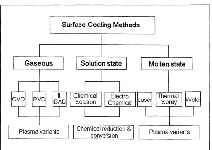
[image:16.616.77.509.409.715.2]The demands from industry to produce components capable of operating in extreme working environments with high performance and enhanced efficiency has provided a large increase in the research and development of surface engineering techniques. Most surface engineering methods rely on the fabrication of a composite system (i.e.thin coating deposited on a substrate) to cause a surface modification which improves the engineering performance to a level which cannot be achieved by either the coating or substrate alone (1). However, some techniques create improved component properties and greater longevity by physical alteration of its surface through diffusion, substitution or implantation of extrinsic atoms to controllable matrix depths. Other methods cause substrate hard-facing through various spraying and welding treatments, whilst many processes utilise a mechanical approach (shot-peening and polishing) to improve wear properties and enhance repair efficiency. This large number of surface engineering methods can be categorised by 3 broad generic surface engineering groups (figure 1.1).
Figure 1.1 The surface engineering generic groups
PVD
CVD IBAD ChemicalSolution ThermalSpray Weld
Gaseous
Solution state
Molten state
Electro-Chemical Laser
The diversity of well proven, so-called "wet" surface engineering treatments currently being utilised by industry is vast, ranging from simple painting techniques to more complex electro-plating and salt bath nitriding methods. These traditional techniques have been intensively studied since the early 1900's and exhibit high reproducibility and excellent reliability. However, the wet methods are restricted in the types of coatings they can deposit and can suffer from serious environmental problems.
The last 30 years has seen the emergence of "dry" advanced surface engineering
techniques many of which extensively utilise plasmas to deposit coatings. Most of these techniques have their origins in the semi-conductor and micro-electronics industries where accurate control of the coating composition and growth rate is critical. Nearly all dry methods involve treatment under vacuum conditions in the presence of inert and / or reactive gases and are characterised by high versatility and flexibility in the processing conditions and materials which can be applied.
The applications of surface engineering coatings to industrial components has now become widespread (2) ranging from high technology operations in the compact disc
and aeronautics industries to low technology processes such as the decoration of watch cases and glasses frames. Coatings are routinely used as thermal barriers on gas turbine blades and provide erosion, abrasion, corrosion and oxidation resistance to a wide variety of cutting and forming tools. Anti-reflective coatings are used as filters on many optical devices and thin films have also been produced for their superconducting
properties.
A key dry surface engineering technique showing outstanding scientific and commercial potential in the coating of industrial components is physical vapour deposition (PVD) and will be discussed in greater detail.
1.2. Physical vapour deposition.
The term physical vapour deposition (PVD) covers a multitude of techniques which have the common feature of processing under partial vacuum conditions where at least one of the coating species is atomised from the solid state within a chamber. Generally these methods are plasma assisted and capable of processing at relatively low
temperatures (150-500°C), allowing the deposition of metals, alloys, ceramics and non conducting (radio frequency) coatings to a wide variety of temperature sensitive
substrates. PVD techniques allow unprecedented control of the coating-substrate interface and an ability to tailor the coating characteristics (i.e. thickness,
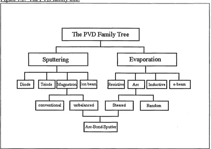
structure and composition) to fine tolerances. Two main deposition methods can be used, sputtering (3-6) or evaporation (7-10) (figure 1.2).
[image:18.614.81.510.195.498.2]Sputter PVD is a process in which the atomisation of coating material is achieved by energetic bombardment of the surface of a solid target with ions or neutral particles. Collisions between the incoming particles and the atoms in the near surface layers of a solid cause complex momentum transfer and the possibility of atomic ejection.
Figure 1.2. The PVD family tree.
lonbeam
Diode Resistive e-beam
Steered
conventional unbalanced Random
Arc-Bond Sputter
Triode Magnetron Arc Inductive
Evaporation Sputtering
The PVD Family Tree
Evaporative PVD is a process in which coating material is produced by either resistive heating, inductive heating, the application of an electron beam or the controlled
interaction of an electric arc with a solid to create joule heating and subsequent evaporation and liberation of metal species into the vapour phase.
Generally, ion or electron beam evaporation takes place under high vacuum conditions
(< 1 0 “5m bar) whilst arc evaporation and magnetron sputtering techniques utilise inert
(Ar) and / or reactive gases (N2) to back-fill the chamber to a total pressure of around
lO'^mbar. A negative bias voltage (50-200V) is typically applied to the substrate during coating, to cause positive ions (usually Ar+) to be accelerated towards the growing film and provide an enhancement in the surface mobility of adatoms, densification of the film micro-structure and a decrease in the level of film roughness.
This thesis will concentrate on the theory, practical arrangement and utilisation of three of the PVD techniques - steered arc evaporation, unbalanced magnetron sputtering and arc-bond sputtering.
1.3. PVD hard coating developments.
The first generation of PVD hard coatings has been extensively studied since the early 1980's and their utilisation in industrial applications has become widespread. This class of coating is characterised by the binary pseudo-ceramic (metal / non-metal compound) materials such as TiN (12), TiC (13) and TiB2(14). Most early PVD fundamental research and applications have centred around the properties and characteristics of the TiN system due to its high hardness, excellent wear resistance and gold colour.
However, interest was quick to spread to the deposition of other transition and refractory metal systems combined with a wide variety of reactive gases (CH4, N2, and O2).
Further developments in coating technology started to occur during 1986 with the introduction of multi-component materials, now considered to be the second generation of PVD hard coatings. Ternary and quaternary (15) films were produced by the addition of further metal elements to the binary systems to form substitutional alloy nitrides and carbides, or by the mixing of reactive gases (N2 & CH4) to produce metal carbo-nitride
films. Research has demonstrated that the use of coatings such as TiAIN (16) or TiCN (17) can produce greater improvements in the engineering performance of a broad range of components when compared against the binaiy systems due to superior hardness, oxidation and wear resistance properties. However, problems have been encountered during the deposition of multi-elemental films in various PVD techniques. Reactive sputtering systems can suffer from target cross-contamination, large differences in sputter yields and preferential target poisoning. Evaporation techniques can suffer from preferential erosion problems, differences in evaporation rates and "spitting".
The latest development in PVD hard coating technology is the production of multi-layer and superlattice thin films (18-20) and is considered to be the third generation. This type of coating can be fabricated in two different classes:
• Metal / ceramic multilayers produced by reactive gas partial pressure control - e.g. Ti/TiN.
• Ceramic / ceramic multilayers produced by reactive co-deposition of different target materials - e.g. TiN/ZrN.
The academic and commercial interest of this type of film lies in their considerably enhanced mechanical and physical properties and crack deflection mechanisms.
However, the present level of understanding in third generation coatings is deficient and industrial scale deposition is still commercially unavailable.
Other emerging coating groups currently under investigation include the superhard (hardness ranging from 5000-10000HV) and low friction coatings. Examples of the superhard class of coatings are diamond, diamond like carbon (DLC), cubic boron nitride (cBN) and carbon nitride films (CN), whilst M0S2 and Si3N4 films show
excellent tribological properties.
1.4. Present work.
At present, knowledge and understanding of the production and characteristics of second and third generation coating systems is far from complete. Arc evaporation systems suffer from preferential erosion problems during the deposition of multi- elemental coatings and provide inefficient utilisation of the target materials. One suggested method to overcome some of the evaporation problems is the use of a segmented target consisting of concentric circular sections into which a cathodic arc may be steered by use of a suitable magnetic arrangement (21-23). The use of a segmented target in sputter PVD may also be a cost effective method for studying preferential poisoning mechanisms prevalent in co-deposition systems.
The recent development of Arc-bond sputter PVD technology has led to a capability to independently coat by both the steered arc evaporation and unbalanced magnetron sputtering techniques. This uniquely allows the combination of two different line-of- sight PVD techniques during a single process and may provide a method for the deposition of low period multi-layer coatings at industrial scale.
Thus, the following three areas were identified in which further research was required:
(i) Fundamental studies on the fabrication and performance of multi-elemental segmented targets in arc evaporation and magnetron sputtering. Specifically to investigate the cathode spot motion across dissimilar metal junctions and examine deformation and interfacial phenomena occurring during steered arc evaporation. Analysis of preferential segmented target poisoning in reactive sputter processes and investigation of the advanced PVD coating properties.
(ii) Critical examination of the second generation TixZryN ternary coating system deposited by unbalanced magnetron sputtering, steered arc evaporation and arc-bond sputter PVD. Study of the production and characteristics of arc-bond sputter TixZryN coatings modified by the addition of Al.
(iii) Development and investigation of a new industrial scale combined arc evaporation / unbalanced magnetron sputter technique for the deposition of third generation
superlattice coatings. Analysis of the relationships between substrate rotation velocity, fold of rotation, superlattice period and the mechanical and physical properties of TiAlN-ZrN and TiAIN-TiN coatings.
This thesis describes work performed in these areas and consists of a further 7 chapters :
• Chapter 2 reviews experimental results and theoretical models obtained from literature and surveys developments in steered and random arc evaporation, conventional and unbalanced magnetron sputtering and advanced coating systems.
• Chapter 3 reviews the experimental techniques employed and a detailed description of the experimental apparatus.
• Chapter 4 consists of experimental work performed on fabrication and performance analysis of segmented targets. This chapter includes results from investigations of target phenomena and coating properties during steered arc and unbalanced magnetron sputter deposition trials.
• Chapter 5 consists of experimental work performed during critical examination of the TixZryN coating system deposited by arc-bond sputter (ABS™), steered arc and unbalanced magnetron sputter PVD. The influence of aluminium substitution in the TixZryN coating lattice and the mechanical and physical properties of the film is also considered.
• Chapter 6 contains a description of a new industrial scale technique for the
deposition of superlattice thin films by combined steered arc evaporation and unbalanced magnetron sputtering. This chapter presents results on the mechanical and physical properties of TiAlN-ZrN and TiAIN-TiN superlattice films and the influence of planetary rotation velocity and the type of rotation on the superlattice period.
References.
1. D.S.Rickerby, A.Matthews - "AdvancedSurface Engineering", 1991, Blackie Press. 2. A.Matthews, RJ.Artley, P.Holliday, P. Stevenson - "The UK Engineering Coatings
Industry in 2005", Department of Trade and Industry / University of Hull, August 1992.
3. B.N.Chapman - "Glow Discharge Processes", 1980, Wiley Interscience Press. 4. J.Musil, S.Kadlec, J.Vyskocil, V.Poulek - Surf.Coat.Tech, 1989, 39-40, 301-314. 5. U.Konig - Surf.Coat.Tech, 1987, 33, 91-103.
6. J.L.Vossen, W.Kem - "Thin Film Processes", 1978, Academic Press.
7. G.Ecker - "Vacuum Arcs - Theory and Application", 1980, Wiley Interscience Press.
8. E.Erttirk, O.Knotek, W.Burgmer, H.-G.Prengel, H.-J.Heuvel, H.G.Dederichs,
C.Stossel - Surf.Coat.Tech, 1991,46, 1, 39-46.
9. P.D.Swift, D.R.Mckenzie, I.S.Falconer - J.Appl.Phys, 1989, 66(2), 505. 10. H.K.Pulker - "Coatings on Glass", 1984, Elsevier Press.
11. W-D.Miinz, F.J.M.Hauzer, D.Schulze, B.Buil - Surf.Coat.Tech, 1991,49, 161. 12. W.D.Sproul, P.J.Rudnik, M.E.Graham - Surf.Coat.Tech, 1989, 39/40, 355-363. 13. P.A.Steinmann, H.E.Hintermann - J. Vac.Sci.Technol, 1985, A3(6), 2394-2400. 14. O.Knotek, F.Loffler, M.Bohmer, R.Breidenbach, C.Stobel - Surf.Coat.Tech, 1991,
49,263-267.
15. O.Knotek, W-D.Miinz, T.Leyendecker - J. Vac.Sci.Technol, 1987, A5(4), 2173- 2179.
16. W-D.Miinz - J. Vac.Sci.Technol, 1986, A4(6), 2717-2725.
17. E.Damond, P.Jacquot, J.Pagny - Materials Science and Engineering, 1991, AMO, 838-841.
18. S.A.Bamett - "Physics o f thin films", 1993,17,1-77, Academic Press. 19. H.Holleck, M.Lahres, P.Woll - Surf.Coat.Tech, 1990, 41, 179.
20. X.Chu, M.S.Wong, W.D.Sproul, S.L.Rohde, S.A.Bamett - J. Vac.Sci.Technol, 1992, A 10(4), 1604-1609.
21. P.Jewsbury, S.Ramalingam, R.F.Chang - Proc. Eng.Mat.Adv.Friction and Wear App.Conf 1988, 107.
22. A.I.Bushik, B.Jiittner, H.Pursch, V.A.Shilov -Akademie der Wissenschaften der DDR, Zentralinstitut fur Elektronenphysik Preprint 83-1, 1983, 1-38.
CHAPTER TWO
LITERATURE REVIEW.
2.1. Sputtering Techniques.
2.1.1. Sputtering processes and energetic particle interactions.
Sputtering is the removal of atomised material from a solid due to energetic
bombardment of its surface layers by ions or neutral particles (1). The phenomenon was first discovered by W.R.Grove (2) in 1842, who noticed the build up of a metallic deposit on the glass walls of a discharge tube. However, it took an additional 50 years before the physical process involved in sputtering was recognised (3) and another 100 years for a quantitative description of the sputtering events to be developed (4-7).
Generally, an incoming particle will collide with atoms at the surface of a solid causing an energy transfer to the atomic nuclei such that:
4 mi mt . 2 © o 1
T = --- j E0 sin — .... equation 2.1
(mi + mt) 2
where T = Energy transfer function for a binary collision. mj and m^ = Masses of the incident and target atoms. © = Projectile scattering angle.
E0 = Initial energy of the atom.
If more energy is transferred than the binding energy at a lattice site, primary recoil atoms may be created which can collide with other target atoms and distribute their energy via a collision cascade. A surface atom becomes sputtered if the energy transferred to it normal to the surface is larger than the surface binding energy (approximately equal to the heat of sublimation).
The ability of a material to be sputtered is measured by a quantity known as the
sputtering yield (Y). This may be simply defined as the mean number of atoms removed per incident particle:
No. of atoms removed
The yield is dependent not only on the characteristics of the target material, but also on the incident angle, ion energy and ion mass and may be approximated (8), assuming
normal incidence, using the equation;
__ 3EtaEi . _ _
Y = — =— equation 2.3.
Uo
where E^ = Energy transferred in a binary collision, a = Function of the colliding atomic masses. U0 = Surface binding energy of the target.
Ej = Energy of the incident ion.
The importance and measurement of the sputtering yield was first recognised around 125 years ago (9) and has been the subject of investigation ever since (10). Whilst the variation in sputtering yield can be as much as one order of magnitude, it is
considerably lower than variations in the evaporative yields from solid and liquid sources, which often reach several orders of magnitude (1 1,1 2) and evaporation
techniques generally provide higher deposition rates. However, sputter processes provide a number of key advantages over evaporative processing techniques
including:-(1) Higher thickness uniformity.
(2) Deposition of a wide variety of materials.
(3) Smooth films (no spitting or macro-particle formation). (4) Large target areas.
The sputtering process has almost no restrictions in the target materials which can be used, ranging from pure metals (d.c power supply) to semi-conductors and insulators (r.f.power supply). Deposition can be carried out in either non-reactive (inert gases only) or reactive discharges (inert & reactive gases) with single or multi-elemental target materials, allowing an extension of the possible combinations and compositions of coatings even further. For more detailed aspects of sputter processing the reader is referred to a series of excellent reviews (13-16) and the later sections of this thesis (section 2.1.2-2.1.4).
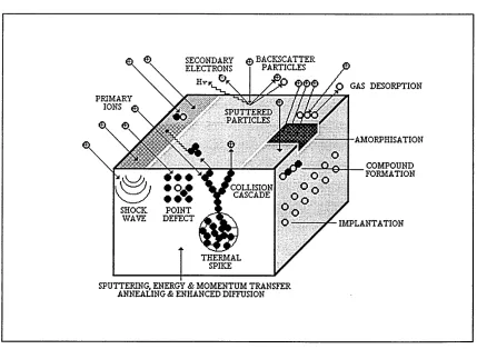
It is important to note that a wide range of other physical interaction events (figure 2.1) at the target surface can be caused by energetic particle bombardment (16).
Possible particle ejection events include liberation of neutral atoms, backscattering, X- ray emission, photon generation, secondary electron emission and desorption of gas atoms. Processes within the target itself include amorphisation, implantation, compound formation, localised heating and the creation of point defects.
Figure 2.1. Interaction events due to energetic particle bombardment.
SECONDARY © BACKSCATTER
ELECTRONS PARTICLES
^ e>
' ' SPUTTERED PARTICLES
1 ” i;:M!'k
^
u
SHOCK POI
WAVE DEEE
A COLLISION
T P CASCADE
NT
JL
:c t
THERMAL SPIKE
GAS DESORPTION
o.
d r
° 0
-AMORPHISATION
COMPOUND 'FORMATION
IMPLANTATION
SPUTTERING, ENERGY & MOMENTUM TRANSFER ANNEALING & ENHANCED DIFFUSION
A number of important processes utilising sputtering and secondary electron emission mechanisms have evolved to deposit thin films and these will be described in greater detail.
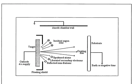
2.1.2. D.C.Diode sputtering - The self sustained glow discharge.
When the accelerated ions reach the target they undergo charge-exchange collisions and lose most of their energy in the form of heat. Momentum is transferred to atoms in the near surface region of the target and creates collision cascades which can cause
[image:27.612.73.503.153.427.2]the ejection of target atoms.
Figure 2.2. Schematic of d.c.diode sputtering.
Anode chamber wall
Incident argon
0 ions Substrate
Target
^Coating > _ O Sputtered atoms
, - Liberated secondary electrons Reflected ions & atoms
Cathode
d.c.supply Earth or negative bias
Floating shield
Another consequence of the ion bombardment is the liberation of secondary electrons from the target which are attracted towards the walls of the vacuum chamber, causing further ionisation events and dissociation and excitation of the argon atoms. Hence a closed circuit is formed and the glow discharge can be made to self-sustain.
The number of secondary electrons emitted per incident ion is termed the "secondary electron yield" and in sputtering processes is typically of the order of 0 .1 (16).
Combined with the low kinetic energy of sputtered particles (~5-20eV), the high percentage of neutrals created by sputtering (>90%) and the poor ratio of energy transferred by incident ions to the number of sputtered particles ejected (~1%) (2 0,2 1),
the diode sputtering process is clearly very inefficient. However, a number of methods to improve the performance of sputtering, based on diode techniques, have recently been developed and will be discussed in sections 2.1.4 to 2.1.6.
2.1.3. Glow discharge characteristics.
Several distinct regions exist within a d.c.diode glow discharge plasma and their
classical architecture is defined in figure 2.3. Directly next to the. cathode is the cathode glow region which is highly luminous due to positive and negative ion neutralisation events occurring at the cathode surface. Adjacent to this is the cathode dark space or "cathode sheath" region, across which most of the potential is dropped, providing the accelerating force necessary to transport positively charged ions from the negative glow towards the target. The dark space region originates from plasma interactions with a surface which is electrically isolated. Initially, the electron flux will be greater than the positive ion flux due to higher random velocities, allowing the surface to acquire a negative potential relative to the plasma. This causes the formation of an electron depleted region adjacent to the cathode surface and creates an enhanced electric field which increases the positive ion flux density impinging on the target surface.
Figure 2.3. Plasma regions within the glow discharge
CATHODE CATHODE
GLOW DARK
SPACE
POSITIVE COLUMN
VOLTAGE
NET SPACE CHARGE
ANODE GLOW
+
FARADAY DARK SPACE
ANODE DARK SPACE NEGA'
The thickness of the cathode sheath can be predicted for d.c. argon discharges from the free-fall version of the Child-Langmuir relationship (22) :
L = (4E0/9J) 1 (2q/mj) 1 ^ y3/4 equation 2.4.
where, L = Sheath thickness, E0 = Permittivity of free space,
J = Cathode current density, q = Ion charge.
mj = Mass of ion, V = Potential drop across cathode sheath.
The cathode sheath is typically a few centimetres thick, and as the negative glow
potential (plasma potential) is only a few volts positive with respect to earth, the voltage drop across the sheath is essentially the same as the bias applied to the cathode.
However, the Child-Langmuir model treats the dark space in isolation and is not fully consistent due to incorrect assumptions on incoming ion velocities, collision theory within the dark space region and electric field suppositions at the dark space-plasma boundary (23).
In most PVD processes the negative glow region fills a considerable area within the chamber. When an ion strikes the target there is a possibility of secondary electron emission (5-10%) along with the generation of heat and the sputtering of atoms. These electrons are accelerated in the opposite direction to the Ar+ ions across the dark space and enter a region where they expend most of their energy in ionising and exciting collisions with argon neutral atoms, sustaining the discharge. Relaxation and de excitation events generate photon emissions at wavelengths characteristic of the
elements present, giving rise to a glow. Beyond the negative glow region is another dark space (Faraday dark space), the positive column (which most resembles a plasma), the anode dark space and the anode. For sputtering plasmas these regions are of lesser importance and are not considered further.
The current-voltage (IV) characteristic of the glow discharge is shown in figure 2.4. Sputter PVD systems aim to work with "abnormal" glow discharge properties, where an increase in power results in a sharp rise in voltage and an optimised increase in the target area carrying current.
Figure 2.4. Glow discharge TV characteristics.
Abnormal Voltage
(V)
Normal glow
Breakdown;
Current
(A)
2.1.4. D.C triode sputtering
Improvements in the ionisation of a d.c. sputtering source can be made by the addition of a third electrode (thermionic emitting filament or a positively biased conductor) into the original diode arrangement. These type of systems are known as d.c. triode
sputtering units (figure 2.5).
Figure 2.5. The d.c.triode sputtering arrangement.
Anode chamber wall
Incident argon
Substrate Target
.Coating
Cathode
d.c. supply Electron
emitter Earth or negative bias
Floating shield
Triode sputtering allows independent variation of the discharge current and voltage, providing full control of increased ion densities impinging on both the substrate and the target (24) and allows deposition at lower pressures and higher rate. However these systems tend to be sensitive to contamination from the thermionic emission electrode and overheating from increased electron bombardment and radiation.
2.1.5. Magnetron enhanced sputtering.
The application of a magnetic field in a glow discharge to trap emitted secondary
electrons close to the target and enhance ionisation probability and deposition rate stems from original ideas by F.M.Penning in 1936 (25). However it was not until the 1970's (26,27) that the principle of crossing electric and magnetic fields was successfully applied to PVD sputtering systems.
The "magnetron" employs a magnetic arrangement positioned behind the target, to provide field lines which penetrate through the dark space and produce a magnetic field parallel to the cathode surface and an electric field perpendicular to the dark space (figure 2.6).
Figure 2.6. Magnetron configuration.
E
Erosion Zone
Target
N
Permanent magnets
Soft iron
A particle of charge(q) travelling with velocity(v) interacts with a magnetic field(B), to produce a force perpendicular to both the magnetic field and the velocity. This
may be expressed mathematically as:
F = q v AB equation 2.5.
As electrons are much less massive (me) than ions, only they are. significantly affected by the weak magnetic fields applied in PVD systems. Under the application of an axial magnetic field, an electron travelling along the axis of the discharge will be unaffected since B and v will be parallel and their vector product will be zero. However, if the electron of mass me is travelling at angle 0 to the magnetic field it will be subjected to a
force BevSin© perpendicular to the field. Thus, the electron will describe a circular motion of radius (r) (assuming there are no collisions) such that:
me(vsin0 ) 2 . _ .
---= Bev sin0 equation 2.6.
In magnetron systems this motion is coupled with a velocity vcos0 parallel to B. Hence the general motion of the confined electrons in front of the target is helical, thereby extending their path lengths and the degree of interactions and ionisation events in the plasma. This increased ion density close to the target produces a considerably higher deposition rate (>500nm/minute) when compared to diode sputtering systems and the electron trapping mechanism provides less free electrons to bombard the substrate surface and chamber walls, resulting in a cooler process capable of coating heat sensitive substrates (28-30).
Many different forms of magnetron configuration exist today, but common types include:
(a) Cylindrical or post magnetrons (31). (b) Hollow cathodes (32).
(c) S-guns (33).
(d) Circular planar magnetrons (34). (e) Rectangular planar magnetrons (35).
Figure 2.7. Schematic of the planar magnetron cathode.
Area of
Erosion Magnetic Field Lines Magnet Poles
Hopping Electrons
Cathode
The conventional planar magnetron has been designed such that a looping magnetic field around the inner and outer magnet pole pieces causes an ellipsoidal "racetrack" erosion area on the target surface. The magnetic field effectively concentrates the glow into a localised area to produce a stable line source which provides high plasma
uniformity (37). Conventional magnetrons offer many advantages over diode and triode sputtering systems, however certain problems still remain inherent with this technique:
(i) Decreases in ionisation at increasing target to substrate distances cause problems in deposited film quality (38,39).
(ii) Three dimensional substrates may suffer from low degrees of ionisation and shadowing. (40).
(iii) Uni-polar arcs may be established due to oxide patches or asperities on the surface of the target (41)
(iv)Void formation at grain boundaries when the substrate current density is low (42). (v) The localised erosion track creates inefficient use of the target material (43).
Recently, a modification to the conventional magnetron arrangement has solved many of these problems.
2.1.6. The unbalanced magnetron.
The amount of substrate ion bombardment in a conventional magnetron sputtering system is a function of the power to the cathode and the distance between the target and the substrate (44) and cannot be independently varied unless an auxiliary source of electrons is applied. This severely restricts the coating range and limits the geometries of substrates which can be accommodated. During the 1980's several research groups worked on modifications to the conventional magnetron to improve its ion
bombardment properties and enhance plasma density at the substrate. In 1985-86 Window and co-workers published several reports on novel magnetron developments (45-48) which became the pre-cursor to the "unbalanced" magnetron sputtering cathode.
A conventional magnetron, in an idealised situation has all of its magnetic field lines looping between the inner and outer magnet pole pieces, and the return field lines contained by the steel yoke on which the magnets are fixed. Generally the magnetic field strength of the inner magnet array is the same (approximately) as the outer array, and this condition is said to be "balanced".
When a conventional magnetron is unbalanced, the strength of one set of magnets, normally the outer set (type II), is increased with respect to the other (49). The result is that the plasma formed is not confined close to the target surface but expands away due to the formation of a trumpet shaped magnetic field profile (figure 2.8), considerably
increasing the substrate ion bombardment intensity such that it is comparable to other high deposition rate techniques (20). Experimental measurement and computer modelling of magnetic field and plasma profiles has been undertaken (50,51),
confirming theoretical calculations on field shapes and throwing distances and revealing ion to deposited atom ratios greater than the order of 2 :1 even at low substrate bias
Figure 2.8. Conventional and unbalanced magnetron configurations
Conventional balanced magnetron
Unbalanced magnetron
Since 1986 various research groups throughout Europe and the USA directed by Musil and Kadlec (52-54), Miinz (55,56), Teer (57) and Sproul (58) have made contributions to advance unbalanced magnetron technology. Today, unbalanced magnetron sputtering systems can produce high quality coatings at target to substrate distances in excess of 200mm with bias current densities greater than 2mAcm~2 and high deposition rate. However, the single unbalanced magnetron coating system has not solved all of the problems which conventional balanced magnetrons suffer from (section 2.1.5). The line of sight nature of the sputtering process means that variation in coating thickness uniformity and shadowing of complex 3-dimensional geometry can still occur. These problems have now largely been eradicated with the development of multi-cathode deposition systems using planetary substrate rotation mechanisms.
2.1.7. Multi-cathode systems and closed field geometry.
When a pair of unbalanced magnetron cathodes are mounted in a vacuum chamber, the spatial arrangement of the magnet arrays has a large effect on the plasma confinement characteristics (59). Generally two geometrical positions are possible (figure 2.9) :
(a) Mirrored - where like poles face each other.
(b) Closed field - where opposite poles face each other.
Figure 2.9. Schematic diagram of mirrored and closed field geometry.
Mirrored configuration Closed field configuration
Substrate Substrate
NillilSI IS N
Field lines Field lines
Investigations on mirrored configuration sputtering have shown that the plasma ion densities were generally very low and substrate bias current densities were typically less than lm A cm " 2 (60 ) resulting in a porous coating microstructure and poor adhesion. If
the magnets were arranged in the closed field configuration, where the field lines from one set of magnets are directly coupled to the opposing magnet array, large increases in bias current density (> 6m A cm "2) and ionisation at the substrate could be achieved. The
linking of the magnetic field lines also provides a high degree of plasma confinement and exact control of the deposition region (61).
Most PVD systems now also utilise 2-fold or 3-fold planetary substrate rotation systems to provide high coating uniformity and the suppression of shadowing effects (64). Here each individual substrate, its holder and the entire rotation assembly circulates at different angular velocities due to a complex gearing mechanism.
2.1.8. Reactive sputtering.
Reactive sputtering involves the introduction of a reactive gas into the plasma during deposition to activate dissociation and ionisation of the gas molecules and allow
combination with the metal vapour flux to produce compound formation at the substrate surface (65-68). Many reactive gases can be used to deposit a wide range of desired compounds, for example nitrogen to form nitrides, methane or acetylene to produce carbides or mixtures of both nitrogen and methane to yield carbo-nitride films. However, the reactive sputtering process is normally non-linear where often it is not possible to change one parameter without affecting others.
When a high reactive gas partial pressure is applied to a sputtering system, reaction can take place not only at the substrate but also the target surface due to chemisorption until, if a sufficient partial pressure is available, the target itself becomes completely covered with the depositing compound and the compound is sputtered instead of the pure metal. This phenomenon is known as "poisoning" (69). As the compounds often have much lower sputtering and secondary electron yields than the pure metals (70), the result is usually a drastic reduction in the deposition rate and ionisation within the plasma. Conversely, if the partial pressure of the reactive gas is too low, an insufficient quantity of gas atoms are available to react with the metal vapour flux and a sub-stoichiometric film is produced. The critical partial pressure required to produce a stoichiometric film without poisoning the target can be found by plotting the reactive gas partial pressure or the deposition rate against the reactive gas flow.
Figure 2.10 The reactive sputtering hysteresis effect.
■Critical point
Critical point
Nitrogen flow
Figure 2.10 illustrates the unstable region in which the critical partial pressure point lies and the hysteresis effect common to all reactive sputtering systems. A substantial drop in metal vapour at the onset of target poisoning is clearly visible, resulting in a further excess of reactive gas (in this case N2) which serves to rapidly stabilise the
process at a rate minimum. If the reactive gas partial pressure is subsequently lowered, the sputter yield only gradually recovers back to that of the pure metal due to the removal of the target surface compound, providing the evident mis-alignment of the upward and downward reaction behaviours. Many techniques to accurately control the reactive gas partial pressures have been developed. During the early 1980's Aronson et al (71) demonstrated a reactive gas pulsing method capable of producing non-
homogeneous nitride films of deposition rates at around 70% of the pure metal rates. However, a major development in composition control came in 1984 with the use of automated flow control using fast feedback loops (72). Today, even more sophisticated methods are commonly available including:
(i) Plasma emission monitors (73). (ii) Optical gas controllers (74).
(iii) Mass spectrometer controllers (75).
2.2. Arc evaporation techniques.
2.2.1. The random cathodic arc
An arc may be defined as a discharge of electricity, between two electrodes in the presence of a gas or vapour, that has a voltage drop at the cathode of the order of the minimum ionising or exciting potential of the gas or vapour (79). The process is characterised by the striking of a high current, low voltage arc on a cathode (target) which gives rise to a small, but highly active emitting area (cathode spot) which produces a high velocity jet of vapourised cathode material. The plasma jet intensity peaks in a direction normal to the cathode surface and contains a high proportion of multiply charged ions (80,81), neutral particles, clusters and macro-particles (82-84). Theoretically, the arc is a self-sustained discharge capable of supporting large currents by its own mechanism of electron emission from the cathode and positive ion re bombardment under high vacuum conditions (figure 2.11). If a suitable reactive gas is introduced into the chamber, dissociation, ionisation and excitation can occur during interaction with the ion flux and compound film deposition results.
Figure 2.11. Cathodic arc vapour flux.
Anode
Neutrals
Ion target bombardment
Dense plasma region; T arget or
cathode Metalions
Metal ions
Macro-particles
Without the influence of an external magnetic field, the cathode spot moves rapidly across the surface of the cathode in a random manner and evaporates microscopic points and protrusions to cause craters. However, if the cathode spot stays at an evaporative point for too long, it can generate a minute liquid pool of molten cathode material. This can become vigourously evaporated to a point where micro-explosions can eject
relatively large masses of molten material which condense during vacuum transportation and land on the surface of the substrate to form macro-particles which can be
detrimental to the coating performance.
Original work on random arc evaporation appears as early as 1939 by Burkhardt (85) and was further modified into arc evaporative PVD technology by workers in both the USA (8 6) and USSR (87,88) in the 1970's. Since this time the parameters and physical
properties of the cathodic arc discharge have been intensively studied. Some of these parameters can be easily measured and are not the subject of any great contention, however, others are the subject of a great deal of dispute and are highly significant. The following sub-sections of this thesis will review in more detail the properties of the cathodic arc by experimental and theoretical analysis from literature on the following:
(a) The spot life cycle.
(b) The types of cathode spot.
(c) The spot diameter and current density. (d) Spot splitting.
(e) The types of erosion (f). The random spot motion.
2.2.2. The cathode spot life cycle.
Guile and Jiittner (89) have demonstrated that the cathode spot life cycle can be described by a four stage process consisting of surface explosion, melting and deformation of liquid, crater formation and quasi-steady state, followed by new spot ignition (figure 2.12). In the first stage, surface explosion, the application of a high voltage between anode and cathode leads to the rapid heating and evaporation of the cathode material, formation of a vapour cloud and electrical breakdown via the
the plasma cloud combined with field rupture or surface tension on the molten liquid pool formed serves to produce hemispherical crater deformation. Stage three involves the main life-time (-lO'^S) of the spot which is spent constantly evaporating material from within the crater with high spatial distribution and high kinetic energy (~100eV).
Figure 2.12. The cathode spot life cycle.
(^Plasma cloudT^)
Stage 1 Surface explosion Stage 2 Melting and deformation
(^Plasma cloudP^)
\ s
Stage 3 Crater formation Stage 4 New spot ignition
After some time it is believed that the spot extinguishes and a new one ignites to take its place, completing stage four and the entire life cycle. Ecker (94) has suggested a model to describe stage four, where heating from the cathode spot gives rise to a localised increase in cathode resistance and the formation of lower voltage sites at locations near the original spot position. A balance must be achieved between the level of heating required to start a new spot and the unfavourable conditions offered by the rise in local resistance. The result is the formation of energetically more favourable spot positions at which the new spot ignites causing the old spot to extinguish.
2.2.3. The types of cathode spot.
Rakhovskii first identified that two different types of cathode spot generally exist, types I and II (95), which have distinct differences in their evaporative behaviour (96,97).
Type I spots only occur on contaminated cathodes with some degree of surface roughness and are characterised by:
(i) Field emission of electrons from micro-protrusions below the spot plasma. (ii) Spot movement occurs by jumping from protrusion to protrusion.
(iii) The mean distance jumped by the spot is greater than the mean crater radius. (iv) Velocity of the spot motion is governed by the plasma expansion.
(v) Non-characteristic arc colour due to weak interaction with the bulk material.
Type II spots may exist in tandem with type I spots and are generally found on clean or conditioned cathodes. During the initial stages of the arcing process a change from type I to type II spot normally occurs and the type II spots are characterised by:
(i) Thermal emission of electrons from the crater to sustain the arc. (ii) The active evaporation area has a lower velocity than in type I.
(iii) The mean distance jumped by the spot is of the order of the mean crater radius. (iv) The colour of the arc is characteristic of the cathode material.
2.2.4. The spot diameter and current density.
The measurement of the spot size and subsequent evaluation of the current density has proved very problematic due to the microscopic nature of the sub-spots (98) which make up the cathode spot and the plasma cloud obscuring optical evaluation. Two different methods to determine the dimensions of the spot are currently used - "autograph" methods (95) which analyse the craters left on the cathode and "fast registry" methods (99) which use high speed photographic techniques to examine the luminous plasma cloud region over the spot. Each evaluation method produces slightly different data due to the limitations of each technique, however typically the cathode spot diameter is of the order of 1 0"^m (1 0 0) and the current densities used in current
random arc PVD equipment are approximately 1 0^-lO ^A m '^ (90,101).
2.2.5. Spot splitting.
As mentioned in section 2.4.4, the cathode spot consists of a sub-structure composed of sub-spots or cells. When the arc current is increased the number of cells increases accordingly until at a certain current limit another large spot begins to form (1 0 2).
In many materials the number of spots which can be formed at high arc currents can be as high as 2 - 2 0 and various models to predict and understand this phenomenon have
been developed. The most consistent models treat sub-spot fission by considering the repulsive electrostatic forces between two dipoles in competition with the attractive magnetic forces between two current carrying conductors (1 0 2) and obtain good
agreement with experiment.
Figure 2.13. The number of cathode spots as a function of arc current.
Number of
cathode spots - B i x-Zn +-A1
o-Cu
2C-100 1000
Current (A)
2.2.6. The types of erosion.
The erosion rate of a random arc on a cathode is a function of the following variables: (i) arc current, (ii) erosion time, (iii) cathode dimension, (iv) gas pressure. However, the parameter which influences the erosion most is the type of cathode spot.
Type I spots have been found to leave craters of 10"^m typical radius and depth with a constant erosion rate per coulomb (electric transfer factor) for degassed cathodes (103). Type II spots exhibit quite different behaviour, with average crater depths of the order of 2.5x10"^m and groups of spots producing trails with depths of 10"^m, indicating the electric transfer factor is substantially dependent upon arc current.
The erosion rate reaches a minimum when arcing occurs under conditions which only allow the type I spot to exist, whilst operation when only type II spots can exist results in a substantial increase in the erosion rate. This can be explained by the different spot electron emission mechanisms.
2.2.7. The random spot motion.
A prominent feature of the cathode spot in the absence of external magnetic fields is its rapid, dynamic and random motion over the surface of the target material. The most consistent models consider the cathode spot movement as a random walk and describe a probability density function for the spot's location.
Daalder (104) assumed that the cathode spot starts to move from the origin of an x-y coordinate system such that during each time interval (T), the spot displacement was a step +s or -s along the x-axis and +s or -s along the y-axis. There is an equal probability that the step is +s or -s in each direction and movement along the x and y axis is
stochastically independent. After n sets of displacements the spot position is (x,y) at time t, hence we take t = nT. Thus the probability that after n steps at time (t) the spot position in x (i.e one dimensional random walk) is given by the normal density
function:-1 x2
P(x) = 77—( TT77exP- (— ) ....equation 2 .7
2mxt) 2a t
where a, the diffusion constant = (s^/T), provided n is large and in two independent random walk
processes:-p(x,y) = p(x)p(y) equation 2 .8
Thus;
1 x2 + y2
p(x, y) = ---exp- (---- —) ...equation 2.9
27iat 2at
by:-R R2
p(R) = — exp( ) equation 2.10
at 2a t
2.2.8. The steered cathodic arc
The random arc evaporation technique suffers from the serious disadvantage that in addition to the plasma jet, the arc produces a spray of liquid droplets or macro-particles which can be tens of microns in diameter (82) and detrimental to surface quality and film adhesion. One method to decrease macro-particle incorporation in the coating is to increase the velocity at which the cathode spot moves and hence decrease the spot dwell time and molten pool dimensions. The steered arc system uses a magnetic field to control the motion of the cathodic arc (figure 2.14), which is essentially a current carrying conductor, and force the cathode spot along a pre-determined closed path defined by the position of the normal field component zero (105).
Figure 2.14 The transverse and normal field profiles from a single coil steering system
Position ( nun
mT
-10
-20
The first commercial PVD systems used a fixed permanent magnet array to steer the arc in a circular orbit (106). However, further developments to enhance cathode usage were
made by Interatom GmbH to provide rosette shaped arc paths by means of various motorised rotating magnets (figure 2.15). More recently Morrison (107) has utilised transient steering fields generated by electromagnetic coils to bounce the arc back and forth along a channel and Walke et al (108) have produced a two coil system which allows pre-selection of the arc track radius and highly efficient utilisation of the entire cathode material.
Figure 2.15. Schematic of Interatom permanent steered arc path.
R o s e tte p o tterr
oF s t e e r e d a r c ,C athade
A rea o f c a th o d e c o v e r e d by a r c R adius oF ✓
o s e t t e p ath
All magnetic steered arc systems rely on the physical phenomenon that if a transverse magnetic field is applied from behind an arc evaporation cathode, a "Lorentz force" will be exerted on the arc such that:
v ~ -j A B equation 2.11 or,
F ~ q[ |Bpj - (B-j)B ] equation 2.12 where; F = Force.
q = Moving charge, j = Current.
However, rather surprisingly at magnetic field strengths of up to one Tesla and chamber pressures below a critical value (1-60 Torr, depending upon working gas ) the arc moves in the non-amperian (-j A B) or retrograde direction (105,109,110). The most consistent models which have been developed to explain this, consider the superposition of self fields (generated by the electron current from the spot) and applied transverse fields which combine favourably on the retrograde side of the cathode spot to cause
asymmetric plasma confinement (figure 2.16), more intense ion bombardment and the production of more favourable electron emission sites (111). Several other authors have used the movement of space charge (1 1 2), movement of the spot plasma (113) or
bending of the plasma column (114) to explain the non-amperian behaviour.
Figure 2.16. Asymmetric confinement of the cathode spot.
Plasma ,
Direction of arc motion
Cathode Crater
Self-field combines Self-field substracts with applie d field and j
confines plasmaapplied field and fiom applied field andand confines expands plasma
The velocity dependence of a high current arc (2.7-6.9KA) as a function of the magnetic self-field strength is shown in figure 2.17 (115). Investigations have revealed an almost linear dependence with inherent field strength up to a velocity threshold of ~30ms"l(for copper cathodes) for fields up to 4xlO“^T. If strong external transverse fields are
applied (Ixl0"l-1T) significant increases in arc velocity up to 500-1000 m s'l have been recorded until at around 1 Tesla, a sharp transition from retrograde to amperian motion has been observed (114). The arc velocity decreases with increasing cathode
temperature (116), thus creating more macro-particles and has also been found to have a complex dependence with arc voltage, thermal conductivity and cathode material.
Figure 2.17. Arc velocity as a function of self-magnetic field strength.
30
25
20
Velocity (ms'1)
Most steered arc systems provide secondary confinement of the arc on the cathode surface by means of a passive border with predetermined electrical characteristics. The primary requirements of the border material is that it should have a very low secondary electron yield which promotes new spot ignition sites back on the cathode surface and that it provides high arc stability for operation over long periods of time. The material which is generally chosen for passive confinement is boron nitride.
Reactive steered arc evaporation processes are generally less sensitive to poisoning and require less complex gas partial pressure control than in sputtering systems. However, if high partial pressures of gas are applied cathode poisoning can occur and for certain modified processes is actively used to provide lower levels of macro-particle formation from the compound (117).
Mechanical or electrical changes to the magnetic field profiles allows precise movement and selection of the radius of the arc track (in circular geometry) on the surface of the cathode and provides various advantages over random arc
systems:-(i) Exact control over the emission area.
(ii) Elimination of periodic extinguishing or "quenching" at low current densities. (iii) Significant reduction in the production of macro-particles generally giving better