Available online: http://edupediapublications.org/journals/index.php/IJR/ Page 13
Design of Area and Power Efficient VLSI Architecture for MAC
Based FIR Filter
B.Narendra (Research Scholar) 1, B. Lokeshwar Reddy2 (Assistant professor) Golden Valley Integrated Campus, Angallu, Madanapalli
ABSTRACT
Finite Impulse Response (FIR)
filters are the most popular type filters in a
typical digital filter application on a
Digital signal processing (DSP) reads a
input samples from an A/D converter,
performs the mathematical manipulations
dictated by theory for the required filter
type and outputs the result via a D/A
converter. Digital filters uses finite
precision to represent signals and are differ
from analog filters as digital filters uses
finite precision arithmetic to compute the
filter response. In this project, FIR filter is
implemented in Xilinx ISE using
VERILOG language. VERILOG coding
for the FIR filter is implemented in this
project and waveforms are observed
through simulation. Due to the explosive
growth of multimedia application, the
demand for high performance and low
power DSP is getting higher and higher.
Most widely used fundamental device
performed in DSP system is FIR digital
filter.Being the critical implementation,
FIR filter design using MAC
implementation continues to be a critical
area of on-going research activities. For
better performance it is good direction to
optimize power consumption, reduction in
computational complexity as well as area
optimization of FIR digital filter.
Key Words: FIR filter, MAC, registers,
multiplexer and accumulation.
I. INTRODUCTION
Digital filters are used extensively
in all areas of electronic industry. This is
because digital filters have the potential
to attain much better signal to noise ratios
than analog filters and at each
intermediate stage the analog filter adds
more noise to the signal, the digital filter
performs noiseless mathematical
operations at each intermediate step in the
transform.
The digital filters have emerged as
a strong option for removing noise,
shaping spectrum, and minimizing
inter-symbol interference in communication
architectures. These filters have become
popular because their precise
reproducibility allows design engineers to
achieve performance levels that are
Available online: http://edupediapublications.org/journals/index.php/IJR/ Page 14 Digital Filters can be constructed from 3
fundamental mathematical operations.
Addition (or subtraction),
Multiplication (normally of a signal by a
constant) and Time Delay i.e.: delaying a
digital signal by one or more sample
periods. Figure 1. Shows a graphical
means of describing a digital filter
whereby the behavior of the filter is
described by using the mathematical
operations mentioned above.
Figure 1.Block diagram of a Simple
Digital Filter
The Impulse Response of a digital
filter, h(n) is the response of the filter to
an input consisting of the unit impulse
function, δ(n). If the impulse response of
a system is known, it is possible to
calculate the system response for any
input sequence x(n). By definition, the
unit impulse is applied to a system at
sample index n=0. So, the impulse
response is non-zero only for values of n
greater than or equal to zero i.e. h(n) is
zero for n<0.
This impulse response is said to be
causal otherwise the system would be
producing a response before an input has
been applied. It is known from the
time-invariance property of a Linear Time
Invariant System that the response of a
system to a delayed unit impulse δ(n-k)
will be a delayed version of the unit
impulse, i.e. h(n-k).
It is also known from the linearity
property that the response of a system to a
weighted sum of inputs will be a weighted
sum of responses of the system to each of
the individual inputs. Therefore, the
response of a system to an arbitrary input
x(n) can be written as follows:
II. CONVENTIONAL FIR FILTER
The design methods of FIR filter
based on approximation of ideal filter. The
ensuing filter approaches the perfect
characteristic because the order of the
filter will increase, so creating the filter
and its implementation additional
complicated. The design process starts
with necessities and specifications the FIR
filter. The method used in the design
process of the filter depends upon the
implementation and specifications.
There are many advantages and
Available online: http://edupediapublications.org/journals/index.php/IJR/ Page 15 Thus, it is very significant to elect the right
method for FIR filter design. Due to
efficiency and simplicity of the FIR filter,
most commonly window method is used.
The other method sampling frequency
method is also very simple to use, but
there is a small attenuation in the stop
band.
A FIR filter is used to implement
almost any type of digital frequency
response. Usually these filters are designed
with a multiplier, adders and a series of
delays to create the output of the filter. The
following figure shows the basic FIR filter
diagram with N length. The result of
delays operates on input samples.
The values of hk are the
coefficients which are used for
multiplication. So that the o/p at a time
and that is the summation of all the
delayed samples multiplied by the
appropriate coefficients. The filter design
can be defined as; it is the process of
choosing the length and coefficients of
the filter. The intention is to set the
parameters so that the required
parameters like a stop band and pass band
will give the result from running the
filter.
Figure2: Logical Structure of FIR
Filter
III. FIR FILTER USING MAC
As the conventional FIR filter
contains multipliers and adding blocks
.An n-tap FIR filter will consists of ‘n’
number of multipliers and ‘n-1’ number
of adders .Conventional FIR filter lags
back for its complex structure and
consuming more area. This Is because the
n tap filter will have n number of
multipliers which consumes much area
because of its complex and wide
structure, and in additional to that the n-1
adders also add up the area.
considering this as the challenge
the proposed work is done in building
efficient FIR filter by using MAC
Available online: http://edupediapublications.org/journals/index.php/IJR/ Page 16 architecture is employed in the efficient
FIR filter because of its simple structure.
The MAC employed in the FIR filter is
shown below.
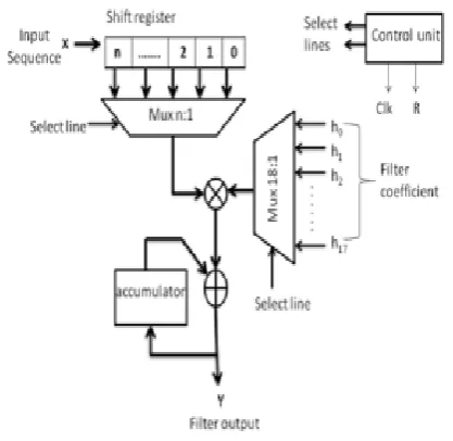
Figure 3: FIR filter with MAC
The architecture of MAC based
FIR filter involves design of following
elements
a. Shift register: This is serial in parallel
out shift register. The effect of each clock
pulse is to shift the data contents (x) of
each stage one place to the right.
b. Multiplexer: multiplexer or mux is a
device that selects one of several analog
or digital input signals and forwards the
selected input into a single line. Proposed
architecture involves design of two mux
one is to select data(x) and another to
select filter coefficients (h). Selected
input is depending upon the logic on
selector pins.
c. Multiplier: The output of two
multiplexer is fed to multiplier. This
multiplier takes 8 bit input and produces
16 bit output.
d. Adder: It adds multiplier output with
previous result stored in accumulator.
Output of adder is taken as filter output
for current sample and also fed to the
accumulator for next input sample.
e. Accumulator: It is 32 bit D flip flop
used to hold the result. With each clock
existing value in accumulator is replaced
by new one.
f. Control unit: This unit is of great
importance as it controls all clock, reset
signal associated with various elements as
shown in fig 3 as well as logic on selector
pins. The working of the control unit
done by the software .and the selection
lines all are generated in the software.
A) WORKING OF MAC
In a FIR context, a MAC is the
operation of multiplying a coefficient by
the corresponding delayed data sample
and accumulating the result. FIR usually
requires only one MAC per all taps. High
speed and high throughput
Multiplier-Accumulator (MAC) unit that consumes
low power, which is always a key to
achieve a high performance digital signal
Processing system.
A low power MAC unit can be
designed and implemented using block
Available online: http://edupediapublications.org/journals/index.php/IJR/ Page 17 MAC unit, data flows from the input
register to the output register through
multiple stages such as, multiplier stage,
adder stage and the accumulator stage.
Within the multiplier stage, further, there
are multiple stages of addition.
During each operation of
multiplication and addition, the blocks in
the pipeline may not be required to be on
or enabled until the actual data gets in
from the previous stage. In block enabling
technique, the delay of each stage is
obtained. Every block gets enabled only
after the expected delay. For the entire
duration until the inputs are available, the
successive blocks are disabled, thus
saving power.
IV. RESULTS
Figure4: RTL Schematic
Figure5: Internal structure of RTL
Schematic
Figure6: View technology schematic
Figure7: simulated wave form
Parameter Existed design
Proposed design No of LUTs 145 46 Power
(mWatt)
Available online: http://edupediapublications.org/journals/index.php/IJR/ Page 18
Table1: parameter comparison table
Figure8: LUT comparison bar graph
Figure9: power comparison bar graph
V. CONCLUSION
The proposed work done in this
paper by implementing the FIR filter by
MAC unit has experimentally reduced the
area because of its simple structure.
Usage of one multiplier and only one
adder is done which is called MAC By
enabling the enable signal of MAC the
multiplication and addition process is
done. After first step operation, The
accumulator is stored then cleared, so that
multiplication and addition can done with
present inputs.
Multiplication and addition is done
in serial rather than parallel .In
conventional FIR For n taps need n
multipliers and n-1 adders, But in our
architecture we need just a multiplier and
one accumulator .So proposed design can
be said to be area efficient. The area is
calculated in terms of the LUTs and based
on the LUTs the power consumption is
also estimated, therefore the proposed
architecture is said to be area and power
efficient.
REFERENCES
[1] A. Belghadr and G. Jaberipur, “FIR
filter realization via deferred endaround
carry modular addition,” IEEE Trans.
Circuits Syst. I, Reg. Papers, to be
published, doi:
10.1109/TCSI.2018.2798595.
[2] P. K. Meher and T. Stouraitis,
Arithmetic Circuits for DSP Applications.
Hoboken, NJ, USA: Wiley, 2017.
[3] L. Wanhammar, DSP Integrated
Circuits. New York, NY, USA:
Academic, 1999.
[4] M. Kumm and P. Zipf, Multiple
Constant Multiplication Optimizations for
Field Programmable Gate Arrays.
Wiesbaden, Germany: Springer, 2016.
[5] X. Lou, P. K. Meher, Y. Yu, and W.
Available online: http://edupediapublications.org/journals/index.php/IJR/ Page 19 Trans. Circuits Syst. II, Exp. Briefs, vol.
64, no. 10, pp. 1212–1216, Oct. 2017.
[6] Y. Voronenko and M. Püschel,
“Multiplier less multiple constant
multiplication,”ACM Trans. Algorithms,
vol. 3, no. 2, p. 11, 2007.
[7] J. Chen, J. Tan, C.-H. Chang, and F.
Feng, “A new cost-aware sensitivity
driven algorithm for the design of FIR
filters,” IEEE Trans. Circuits Syst. I, Reg.
Papers, vol. 64, no. 6, pp. 1588–1598,
Jun. 2017.
[8] F. Feng, J. Chen, and C. H. Chang,
“Hyper graph based minimum
arborescence algorithm for the
optimization and optimization of multiple
constant multiplications,” IEEE Trans.
Circuits Syst. I, Reg. Papers, vol. 63, no.
2, pp. 233–244, Feb. 2016.
[9] J. Chen, C. H. Chang, F. Feng, W.
Ding, and J. Ding, “Novel design
algorithm for low complexity
programmable FIR filters based on
extended double base number system,”
IEEE Trans. Circuits Syst. I, Reg. Papers,
vol. 62, no. 1, pp. 224–233, Jan. 2015.
[10] J. Ding, J. Chen, and C.-H. Chang,
“A new paradigm of common sub
expression elimination by unification of
addition and subtraction,” Microprocess.
Microsyst., vol. 35, no. 10, pp. 1605–