Available online: https://edupediapublications.org/journals/index.php/IJR/ P a g e | 5 4
A bs tract: This paper proposes an innovative method of handling intermittent faults in Network-on-Chip (NoC) embedded memory. A SOA MAT++ test algorithm has been integrated into the NoC router and on-line test has been performed with writing and reading data from FIFO(first in first out). The technique involves repeating tests periodically to prevent accumulation of faults using SOA MAT++. The performance of the NoC are studied in terms of throughput. In addition, detected struck at fault are bypassed for further read and write operation.
Index T erms: FIFO, Intermittent Faults, Network-on-Chip, Router and SOA MAT++.
I. INTRODUCTION
Intellectual Property (IP) based design and advancement in manufacturing technology have allowed today’s Systems-On-Chip (SoCs) according to Benini,De Micheli[8] to include hundreds of embedded cores. In such dense SoCs, the choice of interconnect architecture is a big concern as it governs the performance, power dissipation and cost of the system. Designers using bus based interconnect network for complex System-on-Chip (SoC) designs often face difficulty relating to bandwidth, signal integrity, and power dissipation of the chip. A new communication architecture called Network-on-Chip (NoC) based on Ghoshal et al[1] has been proposed to solve these issues. In a NoC-based chip, the cores communicate among themselves by sending and receiving packets which contain network dependent information required to route the data onto its source of its destination developed by Dally and Towels [9].
The communication network consists of network interfaces, routers and channels which connect the routers. Like all other SoCs, NoC based SoCs must also be tested for defects according to Ebrahimi,et al[2][3]. In majority of works the focus has been to find improved test techniques for minimization of test time and test power at reduced area overhead for logic cores interconnected using NoCS.
The method has been implemented by Soumya et al[4][5]. However, embedded memory content in NoC based systems
has increased from one-tenth to more than three-fourth of the chip area today and will continue to increase. Due to their high density, these embedded memories are more prone to defects than other type of on-Chip circuits. To the best of the knowledge, not much research has been done on exploring test techniques for NoC based memory cores. This brief discusses improved techniques devised for technology-independent functional testing of memory cores interconnected using NoC developed by Petersen and Oberg[6]. Different approaches have been employed for different types of memories, based on their respective fault models and modes of operation. Both off-line and on-line techniques have been proposed for detection of manufacturing faults and run-time faults in memories developed by Barbagallo et al[11][12].to re-use the NoC for testing interconnected cores due to Petersen et al[7] it must be ensured that the elements of NoC are fault free. FIFO buffers present within the routers occupy significant amount of area of the NoC infrastructure. Thus, test of FIFO buffers has major significance in the test of the NoC infrastructure.
This method also proposes improved test technique for memory modules which are part of the NoC infrastructure, namely the Static Random Access Memory (SRAM) based FIFO buffers developed by van de Goor et al [14]. Thus, the work presented in this paper is an attempt to devise cost- effective test techniques, in terms of area overhead, test power and test time for memory modules that are interconnected using NoC as well as part of the NoC infrastructure. According to Van Gageldonk et al[10].
The rest of this paper is to introduce the related work for the paper is discussed in section II. Then, in section III, the proposed system of FIFO buffer of NoC router is discussed. Section IV presents the simulation results of the paper. Finally Section V presents the conclusion of the paper
II. RELA TED W ORK
Memory testing has been a research topic of interest for almost three decades. Researchers over the years have contributed to the three different aspects of memory testing, namely, fault modeling, test algorithm design and memory
An Innovative Method of Handling Intermittent
Faults in Network-on-Chip Embedded Memory
S. Sriramya
#1& G. Sravan Kumar
*2#
M.Tech (VLSI), Department of ECE, BVC College of Engineering, palacharla
Email.id:[email protected].
*
Assistant Professor, Department of ECE, BVC College of Engineering, palacharla
Available online: https://edupediapublications.org/journals/index.php/IJR/ P a g e | 5 5 BIST architectures. Some of the earlier works in fault modeling
such as by Dekker and Goor[14] were limited to static fault modeling. However, with emergence of dynamic faults in memories, fault models for dynamic faults were also proposed in works by Hamidoui. With introduction of fault models, since early 1980s, March tests have become the dominant type of tests for memories. A detailed discussion of different March tests have been covered in several text books such as the one by Van de goor[14]. With advent of technology and emergence of SoCs, accessibility of embedded memory cores has become an issue during testing of SoCs. Thus, BIST has been chosen as the viable test option for embedded memories in SoCs. As a result, over the past decade, a lot of text has been dedicated to design of innovative MBIST architectures. Some of the commonly used MBIST architectures have been covered in books by Bushnell and Agarwal and Wang[7].
Networks-on-Chip (NoCs) developed by Benini and De Micheli[8] constitute a novel design paradigm for high-throughput, scalable on-chip communication in SoCs with billions number of transistors and power management. Asynchronous circuits automatically switch to standby state when they are inactive, and their interesting dynamic power savings has been shown, due to their un-clocked nature according to Van Gageldonk[10]. The Mini-NoC project consists of very simple NoC platforms that are implemented in FPGA with four mMips processor nodes interconnected with a network component in mini NOC website. In a generic On Chip Network (OCN) with many replicated processors and routers, a common fault-tolerant approach is to deactivate the faulty processors and remap tasks on remaining ones in software application is proposed by Petersen and Oberg[6].
According to Xiang[3] the test procedure of a focused on FIFO cushion is started by a counter, which switches the FIFO support from ordinary mode to test mode. NoC should cover communication reliability issues that are essential factor in communication between multiple cores embedded on a chip is described by Ebrahimi[2] defined the controllability or observability of the NoC interconnects is relatively reduced, due to the fact that they are deeply embedded and spread across the chip. The method has been implemented by Kakoee[5] for software applications and hardware architectures described in the DOL tool for performance evaluation.
Significant amount of area of the NoC data transport medium is occupied by routers, which is predominantly occupied by FIFO buffers and routing logic according to Barbagallo[11]. After dealing with failure analysis, an asynchronous First-In-First-Out (FIFO) interface (for multi-clock domain circuits) as an application of the two-D-flip-flop synchronizer is implemented by van de Goor and Zorian[14] Nicolaidis[12] defined the defects in memory arrays are generally due to shorts and opens in memory cells, address decoder and read/write logic. Kundu[4] shows the Simulation results under self-similar traffic show that Mesh of Tree(MoT) enjoys the advantage of having better performance than other
topologies, whereas, it consumes lesser average packet energy than the mesh network that connects single core to each router.
The run-time permanent faults considered in this brief are assumed to be intermittent faults, which have become permanent over time. Consequently, the fault models considered in this brief are that of intermittent faults. The primary factors that lead to intermittent faults are aging effects, such as time-dependent dielectric breakdown (TDDB), electro migration, negative bias temperature instability (NBTI), and hot carrier injection (HCI). TDDB is a phenomenon where the oxide underneath the gate material of an MOSFET degrades over time resulting in a short circuit, which is modeled as stuck-at-faults. Electro migration reduces interconnect conductivity with passage of time and leads to open circuit. The open circuits caused by electro migration are modeled as stuck-open-faults. NBTI and HCI increase the threshold voltage of transistors leading to decrease in mobility. As a result, the performances of the memory core decreases bringing in read and write failures. The write failures are modeled as transition faults, while read failures are modeled as read disturb faults. To summarize, the target fault models considered for this brief are stuck-at fault, stuck-open fault, read disturb fault, and transition fault.
III. PROPOSED SYSTEM
The Significant amount of area of the present NoC data transport medium is occupied by First in First out (FIFO) buffers. Accordingly, the probabilities of faults or defects occurring in buffers are significantly higher compared to the other components of the NoC. Thus, test process for the NoC infrastructure must begin with test of the FIFO buffers. In this work, an on-line transparent test technique has been proposed for detection of run-time faults developed in FIFO buffers present within the routers of the NoC infrastructure. The test performs active fault detection over the entire FIFO buffer. In this work, the FIFO buffers are tested following a Transparent March algorithm instead of conventional March test algorithms to ensure that the memory contents are not lost during test. The Transparent March test is repeated periodically to avoid accumulation of faults in the FIFO buffers. The data traffic moving in and out of the FIFO buffers during normal operation of the NoC is used as data background during test. Thus no data background needs to be loaded in the FIFO buffers prior to testing. A prototype implementation of the test circuit performing the Transparent March test on the FIFO buffers is proposed. The test circuit is integrated into the router-channel interface and the on-line test is performed with different data traffic of different applications.
Available online: https://edupediapublications.org/journals/index.php/IJR/ P a g e | 5 6 Zorian, because the addresses are specified implicitly and
address modification in the form of incrementing is also performed implicitly in SOA. The address order restriction for SRAM type FIFOs and the choice of single order addressing motivated to choose single order address MATS++ test (SOA-MATS++) for detection of faults.
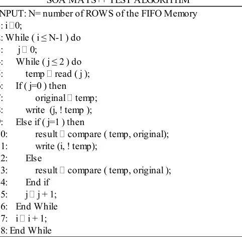
SOA MATS++ TEST ALGORITHM INPUT: N= number of ROWS of the FIFO Memory 1: i 0;
2: While ( i ≤ N-1 ) do 3: j 0;
4: While ( j ≤ 2 ) do 5: temp read ( j ); 6: If ( j=0 ) then 7: original temp; 8: write (j, ! temp ); 9: Else if ( j=1 ) then
10: result compare ( temp, original); 11: write (i, ! temp);
12: Else
13: result compare ( temp, original ); 14: End if
15: j j + 1; 16: End While 17: i i + 1; 18: End While
The algorithmic interpretation of the transparent SOA-MATS++ test is presented in Algorithm. It describes the step-by-step procedure to perform the three phases of the transparent SOA-MATS++ test for each location of the FIFO memory.
For a particular FIFO memory location (present value of i), the first iteration of j (address run1) performs the invert phase, where the content of the FIFO location is inverted. The invert test phase involves reading the content of LUT into a temporary variable temp and then backing it up in original. Then, the inverted content of temp is written back to LUT. At this point, the content of LUT is inversion of content of original.
In the next iteration of j (address run2), the restore phase is performed. The content of LUT is reread into temp and compared with the content of original. The comparison should result in all 1’s pattern. However, deviation from the all 1’s pattern at any bit position indicates fault at that particular bit position. Next, the inverted content of temp is written back to LUT. Thus, the content of LUT, which were inverted after the first iteration get restored after the second.
The third iteration of j performs only a read operation of LUT, where the content of LUT is read into temp and compared with the contents of original. At this stage of the test, all 0’s pattern in the result signifies fault free location, while deviation at any bit position from all 0’s pattern means fault at
that particular bit position. The last read operation ensures the detection of faults, which remained undetected during the earlier two test runs. At the end of the three test runs (iterations of j), the loop index i is incremented by one to mark the start of test for the next location.
Fault Coverage of the Proposed Algorithm:
The transparent SOA-MATS++ algorithm is intended for test of stuck-at fault, transition fault, and read disturb fault tests developed during field operation of FIFO memories. The fault coverage of the algorithm is shown in Fig. 1. In both the figures, the word size of FIFO memory is assumed to be of 4 bits. The text in italics against the arrows indicates the operation performed, while the text in bold font corresponds to the variables used in Algorithm 1.
As shown in Fig. 1, assume the data word present in LUT be 1010. The test cycles begin with the invert phase (memory address pointer j with 0 value) during which the content of location addressed is read into temp and then backed up in the original. The data written back to LUT is the complement of content of temp. Thus, at the end of the cycle, the data present in temp and original is 1010, while LUT contains 0101. Assume a stuck-at-1 fault at the most significant bit (MSB) position of the word stored in LUT. Thus, instead of storing 0101, it actually stores 1101 and as a result, the stuck-at-fault at the MSB gets excited.
Available online: https://edupediapublications.org/journals/index.php/IJR/ P a g e | 5 7 The FIFO buffer present in each input channel of an NoC
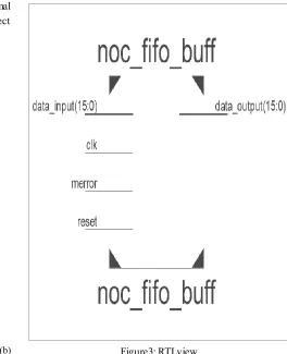
router consists of a SRAM-based FIFO memory of certain depth. During normal operation, data flits arrive through a data_in line of the buffer and are subsequently stored in different locations of the FIFO memory. On request by the neighboring router, the data flits stored are passed on to the output port through the data_out line. Fig. 2(a) shows the FIFO memory with data_in and data_out line. To perform the transparent SOA-MATS++ test on the FIFO buffer, we added a test circuit, few multiplexers and logic gates to the existing hardware, as shown in Fig. 2(a). The read and write operations on the FIFO buffer are controlled by the read enable and write enable lines, respectively. The multiplexer’s mu6 and mu7 select the read and write enable during the normal and test process. During normal operation when the test_ctrl is asserted low, the internal write and read enable lines, wen_int and ren_int, synchronized with the router clock, provide the write and the read enable, respectively. However, during test process, the write enable and read enable are synchronized with the test clock. As mentioned earlier, the read and write operations during test are performed at alternate edges of a test clock. The read operations are synchronized with the positive edges, while the write_clk is obtained by inverting the test clock. In test mode (test_ctrl high), the test read and write addresses are generated by test address generators implemented using gray code counters similar to the normal address generation. Muxes m4 and m5 are used to select between normal addresses and test addresses.
Figure 2: (a) Prototype of the test process for the FIFO buffers. (b) Implementation of test circuit.
Consider the situation when the FIFO buffer is in normal mode with flits being transferred from the memory to the data_out line. After a few normal cycles, the test_ctrl is asserted high, switching the buffer to test mode. As long as the buffer is in test mode, no external data is allowed to be written to the buffer, or in other words, the buffer is locked for the test period. As a result, the input data line for the FIFO memory is switched from the external data_in line to test_data line available from the test circuit. At the switching instant, the flit which was in the process of being transferred to the data_out line is simultaneously read into the Test Circuit. However, a one clock cycle delay is created for the flit to move to the data_out line. This delay ensures that the flit is not lost during the switching instant and is properly received by the router, which requests for it. The single cycle delay in the path of the traveling flit is created by the D-type flip-flop and the multiplexer m3, as shown in Fig. 2(a). The flit, which is read in the test circuit, is stored in a temporary register temp and the test process begins with this flit.
IV. SIMULATION AND RESULT
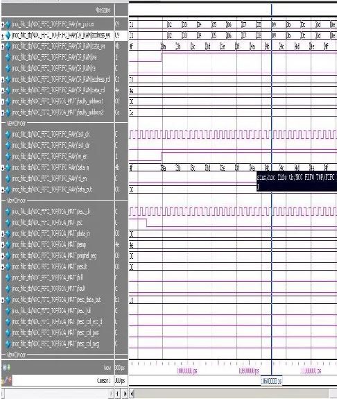
To simulate the proposed system in Mode-lsim and analysis to detect struck at faults and they are bypassed for further read and write operations. The RTL view of the FIFO buffer with NoC is shown figure 3.
Available online: https://edupediapublications.org/journals/index.php/IJR/ P a g e | 5 8 Figure 4 : Simulation result of reading Memory
Figure 5: Simulation result of writing memory
V. CONCLUSION
This paper describes a transparent SOA MAT++ test generation algorithm which detects the struck at faults and they are bypassed further read and write operations of buffer. Hence delay will be reduced and performance is high.
REFERENCES
[1]. ‘In-Field Test for Permanent Faults in FIFO Buffers of NoC Routers’ Ghoshal B. Sengupta I. Manna K. and Chattopadhyay S. IEEE Trans. VLSI Syst., 2015.
[2]. M. Ebrahimi, M. Daneshtalab, J. Plosila, and H. Tenhunen, “Minimal-path fault-tolerant approach using connection-retaining structure in networks-on-chip,” in Proc. 7th IEEE/ACM Int. Symp. Netw. Chip (NoCS), Apr. 2013, pp. 1–8.
[3]. D. Xiang, “A cost-effective scheme for network-on-chip router and interconnect testing,” in Proc. 22nd Asian Test Symp. (ATS), Nov. 2013, pp. 207–212.
[4]. S. Kundu, J. Soumya, and S. Chattopadhyay, “Design and evaluation of mesh-of-tree based network-on-chip using virtual channel router,” Microprocess. Microsyst., vol. 36, no. 6, Aug. 2012,pp. 471–488
[5]. M. R. Kakoee, V. Bertacco, and L. Benini, “A distributed and topology agnostic approach for on-line NoC testing,” in Proc. 5th ACM/IEEE Int. Symp. Netw. Chip, May 2011, pp. 113–120.
[6]. K. Petersen and J. Oberg, “Toward a scalable test methodology for 2D-mesh network-on-chips,” in Proc. Design, Autom., Test Eur. Conf. Exhibit., Apr. 2007, pp. 1–6.
[7]. C. Grecu, P. Pande, B. Wang, A. Ivanov, and R. Saleh, “Methodologies and algorithms for testing switch-based NoC interconnects,” in Proc. 20th IEEE Int. Symp. Defect Fault Tolerance VLSI Syst., Oct. 2005, pp. 238–246 [8]. L. Benini, G. De Micheli, Networks on chips: a new SoC
paradigm, IEEE Computer magzine. 35 (1) (2002) 70–78. [9]. w. j. dally and b. towles, “route packets, not wires:
on-chip interconnection networks,” in proc. 38th annu. design autom. conf., 2001,pp. 684–689.
[10]. H. Van Gageldonk, K. Van Berkel, A. Peeters, D. Baumann, D. Gloor, G. Stegmann, An asynchronous low-power 80C51 microcontroller, in: Proceedings of ASYNC’98, 1998, pp. 96–107
[11]. ‘A parametric design of a built-in self test FIFO embedded memory,’ Barbagallo S. Proc. IEEE Int. Symp. Defect Fault Tolerance VLSI Syst., pp. 221–229,1996. [12]. M. Nicolaidis, “Theory of transparent BIST for RAMs,”
IEEE Trans. Comput., vol. 45, no. 10,Oct. 1996,pp. 1141–1156.
[13]. ‘Using March Tests to Test SRAMs,’ Van de Goor A.J. IEEE Designing & Test of Computers, Vol. 10, No. 1, pp. 8-14, 1993