Scholarship@Western
Scholarship@Western
Electronic Thesis and Dissertation Repository
6-27-2014 12:00 AM
Plasmonic Optical Sensors: Performance Analysis and
Plasmonic Optical Sensors: Performance Analysis and
Engineering Towards Biosensing
Engineering Towards Biosensing
Peipei Jia
The University of Western Ontario
Supervisor Jun Yang
The University of Western Ontario
Graduate Program in Biomedical Engineering
A thesis submitted in partial fulfillment of the requirements for the degree in Doctor of Philosophy
© Peipei Jia 2014
Follow this and additional works at: https://ir.lib.uwo.ca/etd
Part of the Biomedical Devices and Instrumentation Commons, Biotechnology Commons, Membrane Science Commons, Nanoscience and Nanotechnology Commons, Nanotechnology Fabrication
Commons, and the Optics Commons
Recommended Citation Recommended Citation
Jia, Peipei, "Plasmonic Optical Sensors: Performance Analysis and Engineering Towards Biosensing" (2014). Electronic Thesis and Dissertation Repository. 2157.
https://ir.lib.uwo.ca/etd/2157
This Dissertation/Thesis is brought to you for free and open access by Scholarship@Western. It has been accepted for inclusion in Electronic Thesis and Dissertation Repository by an authorized administrator of
(Thesis format: Integrated Article)
by
Peipei Jia
Biomedical Engineering Graduate Program
A thesis submitted in partial fulfillment of the requirements for the degree of
Doctor of Philosophy
The School of Graduate and Postdoctoral Studies The University of Western Ontario
London, Ontario, Canada
ii
Abstract
Surface plasmon resonance (SPR) sensing for quantitative analysis of chemical reactions and
biological interactions has become one of the most promising applications of plasmonics. This
thesis focuses on performance analysis for plasmonic sensors and implementation of plasmonic
optical sensors with novel nanofabrication techniques.
A universal performance analysis model is established for general two-dimensional plasmonic
sensors. This model is based on the fundamental facts of surface plasmon theory. The
sensitivity only depends on excitation light wavelength as well as dielectric properties of metal
and dielectrics. The expression involves no structure-specified parameters, which validates this
formula in broad cases of periodic, quasiperiodic and aperiodic nanostructures. Further
analysis reveals the intrinsic relationship between plasmonic sensor performance and essential
physics of surface plasmon. The analytical results are compared to the sensitivities of
previously reported plasmonic sensors in the field. This universal model is a promising
qualification criterion for plasmonic sensors.
Plasmonic optical sensors are engineered into high-performance on-chip sensors, plasmonic
optical fibers and freestanding nanomembranes. (1) Periodic nanohole arrays are patterned on
chip by a simple and robust template-transfer approach. A spectral analysis approach is also
developed for improving the sensor performance. This sensor is applied to demonstrate the
on-chip detection of cardiac troponin-I. (2) Plasmonic optical fibers are constructed by transferring
periodic metal nanostructures from patterned templates onto endfaces of optical fibers using
an epoxy adhesive. Patterned metal structures are generally extended from nanohole arrays to
nanoslit arrays. A special plasmonic fiber is designed to simultaneously implement multimode
real-iii
take advantages of consistent optical responses, excellent stability during fiber bending and
capability of spectrum filtering. (3) Large-area freestanding metal nanomembranes are
implemented using a novel fabrication approach. The formed transferrable membranes feature
high-quality and uniform periodic nanohole arrays. The freestanding nanomembranes exhibit
remarkably higher transmission intensity in comparison to the nanohole arrays with same
features on the substrate. These three modalities of plasmonic sensors possess different
applicability to fulfill various plasmonic sensing tasks in respective scenarios.
Keywords
surface plasmon resonance, refractive index sensitivity, 2-D nanostructure, periodic,
quasicrystalline, aperiodic, template transfer, nanohole array, nanoslit, plasmonics optical fiber,
iv
Co-Authorship Statement
This PhD thesis has been prepared by P. Jia and reviewed by Dr. J. Yang according to the
regulations for an integrated article format thesis specified by the Faculty of Graduate and
Postdoctoral Studies at the Western University and has been co-authored as follows:
Chapter 3: Universal Optical Performance Analysis
All the theoretical analyses and data analyses were conducted by P. Jia under the supervision
of Dr. J. Yang. A paper co-authored by P. Jia and J. Yang is to be submitted.
Chapter 4: Plasmonic Nanohole Array Sensors Fabricated by Template Transfer
All the experiments and data analyses were conducted by P. Jia under the supervision of Dr. J.
Yang. Dr. J. Sabarinathan provided the optical setup for measurement. Dr. H. Jiang helped to
design and implement optical measurement. A paper entitled Plasmonic nanohole array
sensors fabricated by template transfer with improved optical performance(P. Jia, H. Jiang,
J. Sabarinathan and J. Yang) has been published in the Nanotechnology, 2013.
Chapter 5: Plasmonic Optical Fiber
All the experiments and simulations were conducted by P. Jia under the supervision of Dr. J.
Yang. A paper entitled Integration of large-area metallic nanohole arrays with multimode
optical fibers for surface plasmon resonance sensing(P. Jia and J. Yang) has been published
in the Applied Physics Letters, 2013. Another paper entitled A plasmonic optical fiber
patterned by template transfer as a high-performance flexible nanoprobe for real-time
biosensing (P. Jia and J. Yang) has been published in the Nanoscale, 2014.
v
vi
Acknowledgments
I would like to sincerely thank my advisor, Prof. Jun Yang for his extensive support and
guidance in this research. It is his trust and motivation from beginning to end that enables me
to focus my mind and efforts on my research regardless of challenges and roadblocks at the
moment. The most important thing I have learned from him is how to be an eligible scientist,
which would pave the way for my academic life in future.
Without the help from my colleagues, the research presented in this thesis could not have
happened. I would like to appreciate all generous help from Dr. Tingjie Li, Dr. Qiuquan Guo,
and Dr. Binyu Yu. I express my gratitude to Dr. Meiku Fan for his introduction of this fantastic
field at the very beginning. Other group members also deserve my gratitude for their valuable
comments and suggestions. I am grateful to Dr. Hao Jiang and Prof. Jayshri Sabarinathan for
our successful collaboration to guide me in the right direction. I also thank the staffs from
Western Nanofab including Dr. Todd Simpson, Tim Goldhawk and Dr. Rick Glew for their
technical assistance.
Yet most importantly, my little family gives me happiness, courage and perspective that always
encourage me. I dedicate this thesis and all the hard work it presents, to my wife, Ying, for her
love and all the experience we have gone through together, and to my son, Evan, for his joy
and smile. Finally, I am deeply grateful to my parents and hope they know that without their
endless love, I would never have made it this far.
vii
Table of Contents
Abstract ... ii
Co-Authorship Statement... iv
Acknowledgments... vi
Table of Contents ... vii
List of Tables ... xi
List of Figures ... xii
List of Appendices ... xvii
Chapter 1 ... 1
1 Introduction ... 1
1.1 Surface Plasmon Resonance Sensing... 1
1.1.1 Propagating Plasmon Sensors ... 2
1.1.2 Nanoplasmonic Sensors ... 3
1.2 Fabrication of Plasmonic Nanostructures ... 4
1.2.1 Conventional Top-Down Approaches ... 5
1.2.2 Unconventional Lithography Techniques ... 7
1.3 Motivation ... 11
1.4 Objectives and Outline ... 12
Chapter 2 ... 29
2 Fundamentals of Plasmonics ... 29
2.1 Dielectric Constant of Metals ... 29
2.2 Dispersion Relation of Surface Plasmon ... 30
2.3 Field Penetration Depth ... 33
2.4 Propagation Length ... 35
viii
3 Universal Optical Performance Analysis ... 41
3.1 Performance Characteristics ... 41
3.2 Performance Analysis of Nanohole Array Sensors ... 43
3.2.1 Analytical Performance Modeling ... 43
3.2.2 Analytical Expression of Performance Characteristics ... 45
3.3 Comparison to Localized SPR Sensors... 48
3.4 Sensitivity Qualification ... 49
3.5 Generalization to Quasiperiodic and Aperiodic Structures ... 54
3.6 Conclusions ... 56
Chapter 4 ... 63
4 Plasmonic Nanohole Array Sensors Fabricated by Template Transfer ... 63
4.1 Introduction ... 63
4.2 Experimental Procedure ... 65
4.2.1 Fabrication of Si Template... 65
4.2.2 Transfer of Au Nanohole Arrays ... 67
4.2.3 Optical Measurement ... 69
4.2.4 Cardiac Troponin-I Immunoassay ... 71
4.3 Results and Discussions ... 72
4.3.1 Optical Properties... 72
4.3.2 Optimizing the Sensor Performance ... 75
4.3.3 Using Nanohole Arrays in Biosensing ... 78
4.4 Conclusions ... 80
Chapter 5 ... 86
5 Plasmonic Optical Fiber ... 86
ix
5.2.1 Fabrication and Characterization of Plasmonic Fiber ... 90
5.2.2 Spectroscopic Analysis and Simulation ... 100
5.2.3 Optical Performance ... 104
5.2.4 Self-Assembled Monolayer (SAM) ... 107
5.2.5 Real-Time Biosensing ... 108
5.2.6 Stability, Consistency and Optimization... 111
5.3 Materials and Methods ... 114
5.3.1 Metal Deposition and Transfer ... 114
5.3.2 Fabrication of Flow Cell ... 115
5.3.3 Bulk Refractive Index Sensing ... 115
5.3.4 Biomelecular Sensing ... 115
5.3.5 FDTD Simulations ... 116
5.4 Conclusions ... 116
Chapter 6 ... 122
6 Freestanding Metal Nanomembrane as Plasmonic Sensor ... 122
6.1 Introduction ... 122
6.2 Fabrication of Freestanding Metal Nanostructures ... 123
6.2.1 Preparation for Fabrication ... 123
6.2.2 Fabrication Procedure ... 124
6.3 Characterization ... 126
6.4 Optical Property ... 132
6.5 Conclusion ... 133
Chapter 7 ... 138
7 Thesis Summary and Future Direction ... 138
x
7.3 Future Direction ... 140
Appendices ... 142
xi
List of Tables
xii
List of Figures
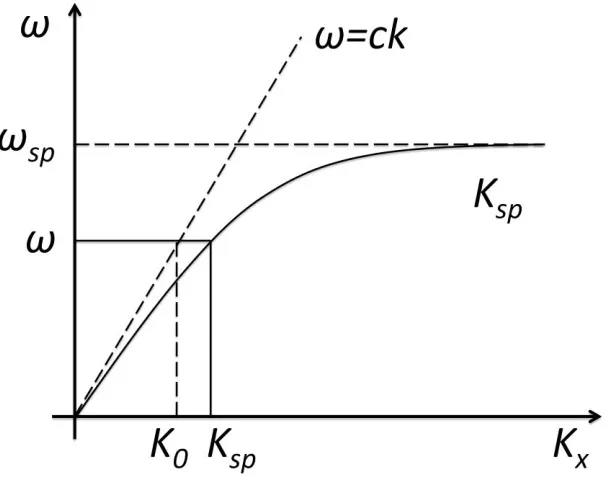
Figure 2-1 Configuration for SPs at an interface between a metal and a dielectric. ... 31
Figure 2-2 Dispertion curve of SP, always lying right of the light line, with surface plasmon
frequency 𝝎𝒔𝒑. ... 33
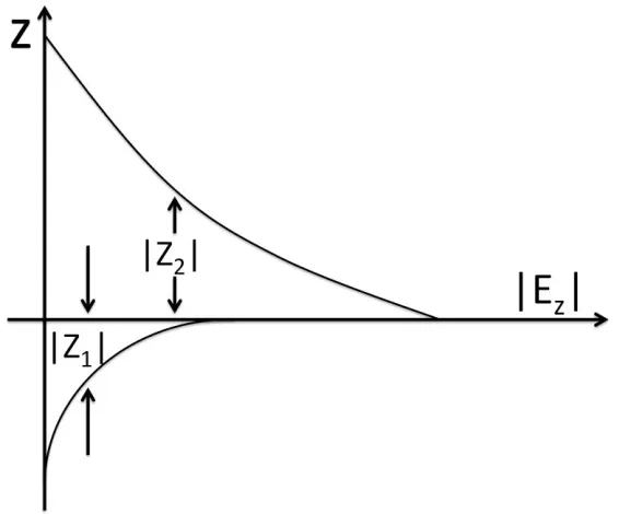
Figure 2-3 Field distribution in the z direction perpendicular to the interface, implying an
evanescent feature. ... 34
Figure 2-4 SPs propagation length of Au and Ag in air and water respectively, showing a strong
dependence on excitation wavelength. ... 36
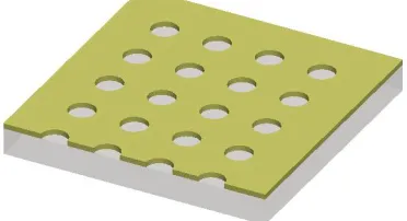
Figure 2-5 Periodic nanohole array supporting extraordinary optical transmission. ... 37
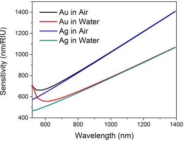
Figure 3-1 Sensitivity of Au and Ag nanohole array sensors in air and water respectively. .. 46
Figure 3-2 Theoretical sensitivities of nanohole arrays and nanoparticles in air. ... 49
Figure 3-3 Theoretical and experimental sensitivities of two-dimensional nanoplasmonic
sensors. ... 54
Figure 4-1 (a) Schematic for the fabrication process of Si templates. (b) Scanning electron
microscope (SEM) image of the Si template with circular pits. Scale bar, 2µm. The diameter
of the nanoholes and the periodicity of the array are 200 and 600 nm, respectively... 66
Figure 4-2 (a) Schematic for transfer of Au nanohole arrays from the Si template to PDMS
xiii
Au film. (c) Enlarged SEM image. The scale bar is 200 nm. ... 69
Figure 4-3(a) Transmission spectra of the nanohole array (hole diameter: 200 nm, periodicity:
600 nm) in a 100 nm Au film stripped by curing PDMS. The refractive indexes of sucrose
solution covered on the Au film vary from 1.3403 to 1.3639. The SEM inset demonstrates the
high magnified nanohole structure. After curing, PDMS blocks nanoholes, keeping their inner
surfaces from external environment. (b) Transmission spectra of the nanohole array transferred
by direct contact with a PDMS slice with the same feature as that in (a). The inset shows the
enlarged SEM image of a hollow hole. (c) Bulk refractive index sensitivity measurements of
the fabricated nanohole arrays. By fitting points of spectral shifts to linear curves, the bulk
sensitivities are determined to be 167 nm/RIU for the peak at 765 nm in (a) and 522 nm/RIU
for the peak at 743 nm in (b) respectively. ... 74
Figure 4-4 Background noise (SD) with the numbers of spectra averaging in tracking peak
positions. The shot noise is reduced to 0.01 nm by averaging 100 transmission spectra. The
inset shows a plot of variation of peak positions for 100 spectra averages. ... 78
Figure 4-5 (a) Optical transmission spectra measurements of the Au nanohole array as a
biosensor. The concentration of cTnI solution incubated on the sensor is 40 nM. (b) SPR shifts
at 600 nm measured after the addition of anti-cTnI, BSA, and cTnI. ... 80
Figure 5-1 (a) Schematic of the fabrication process of plasmonic optical fiber by patterning the
fiber endface. The metal is deposited on the pre-patterned Si template with the designed
nanostructure. After pre-heating the epoxy adhesive on the fiber tip to be sticky, the template
xiv
Two fibers on the right are illuminated by coupling white light from the distant ends. Diameters
of the fiber cores are all 600 µm; diameters of the fiber tips are 3.2 mm (left and right-top) and
6.7 mm (right-bottom) respectively. ... 91
Figure 5-2 (a-c) SEM images of the Au hexagonal nanohole array, square nanohole array and
nanoslit array on the fiber tips. The periodicities of the nanostructures are 700 nm, 600 nm and
500 nm, respectively. All scale bars are 500 nm. (d-f) Photographs of the far-field optical
diffraction patterns produced by correspondingly illuminating (a-c) with white light coupled
from the other bare ends of plasmonic fibers. ... 93
Figure 5-3 SEM images of the Au periodic nanoslits transferred from the same template with
(a) and without (b) the step of pre-heating the epoxy adhesive on the fiber tip. Two images are
aligned vertically for comparison. The dash rectangle highlights the distinct parts for better
visualization. The inset in (b) reveals the epoxy under the Au nanoridges. All scale bars are
500 nm. ... 95
Figure 5-4 Diagram of a Y-shape plasmonic fiber mounted in a flow cell for multimode sensing
simultaneously in transmission and reflection. ... 97
Figure 5-5 Plasmonic optical fibers working in multimode or reflection mode only. ... 99
Figure 5-6 Normalized Au nanohole array spectra for transmission and its simulation as well
as reflection, and the Au film transmission spectrum. ... 101
Figure 5-7 Electric field profiles at peak wavelengths of 494 nm, 538 nm, 585 nm and 698 nm
xv
magnified view of the narrowest resonances in reflection. Refractive index sensitivities (b)
obtained by linear fitting three peak shifts in (a). ... 105
Figure 5-9 Transmission spectra (a) measured in water and NaCl solutions and refractive index sensitivities (b) obtained by linear fitting two peak shifts and two trough shifts in (a). ... 106
Figure 5-10 Optical transmission spectra of nanohole array fibers for SAM assembly. ... 108
Figure 5-11 Real-time peak shifts upon BSA assembly on the plasmonic fiber tip and subsequent binding between BSA and anti-BSA. The red line is a fitted curve for better visualization. ... 110
Figure 5-12 Intensity spectra of a plasmonic fiber for various bending radii from 24 cm to 12 cm. The inset shows the fluctuation of the resonance wavelengths. ... 112
Figure 5-13 Optical transmission spectra of nanohole array fibers with various core diameters in air. ... 113
Figure 5-14 Normalized spectra for single, double and triple plasmonic fibers connected end-to-end. The resonance around 700 nm is narrowed down to 58.2 nm in triple coupling. .... 114
Figure 6-1 Fabrication procedure for freestanding metal nanomembranes. ... 125
Figure 6-2 Freestanding Au nanomembrane on the PDMS holder in a petri dish. ... 125
Figure 6-3 Au nanohole membrane attached on a blade... 126
xvi
Figure 6-6 A narrow and long slit cut by FIB milling. The edge is bent owing to strain release.
After repeatedly imaging with SEM, the slit becomes wider than that at the beginning. .... 129
Figure 6-7 Freestanding nanoslits. The width of the silts is 400 nm. ... 130
Figure 6-8 Transmission spectra of the same nanohole array membrane in freestanding format
xvii
List of Appendices
Appendix 1 Derivation of Sensitivity for a Periodic Nanohole Array Sensor ... 142
Appendix 2 Copyright permission for using article “Integration of large-area metallic nanohole
arrays with multimode optical fibers for surface plasmon resonance sensing” ... 145
Appendix 3 Copyright permission for using article “Plasmonic nanohole array sensors
Chapter 1
1
Introduction
This chapter introduces the basics of surface plasmon resonance sensing and the different
implementation of plasmonic sensors. The advanced nanofabrication techniques used in
plasmonics including top-down lithography and unconventional methods are also
discussed. Based on the limitation of current plasmonic sensing techniques, we define the
objectives and scope of this research.
1.1
Surface Plasmon Resonance Sensing
Surface plasmon resonance (SPR) is collective oscillation resulting from the coupling of
electromagnetic waves with free electrons.1-2 Such interaction is bound to the
metal/dielectric interface and leads to significant field enhancement phenomena. Surface
plasmon (SP) waves are therefore exceptionally sensitive to dielectric properties near the
metal surface. In turn, the refractive index change at the interface will modulate the
high-concentrated electromagnetic fields generated by SPR. This unique aspect gives rise to a
direct means to monitor surface events which could induce dielectric changes for
plasmonic applications.
Typical biosensing related to genomic or proteomic applications with SPR probes rely on
the highly specific binding of a target analyte to a previously immobilized receptor at the
metal sensor surface.3-4 The size of the most common analytes and receptors, such as
process takes place in a few nanometers above the metal surface, where SPR puts the
electromagnetic field into effect. The principle advantage of SPR biosensing is its
‘label-free’ whereby the targets maintain their original properties and functions since no labels,
e.g. fluorescent markers or magnetic beads, are involved.5-6 As a direct consequence,
plasmonic sensors allow for real-time monitoring binding events on the sensor surface,
thereby providing a distinct advantage over endpoint detection methods, such as ELISA
(enzyme-linked immunosorbent assay). This feature constitutes the key of the importance
of plasmonic sensors in biosensing applications.
1.1.1 Propagating Plasmon Sensors
The advances in SPR sensing technology have been remarkable since the introduction of
SPR biomolecular sensing based on propagating SPs on flat thin metal films.7 Meanwhile,
the commercialization of instruments such as Biacore Inc. has significantly expanded the
scope of plasmonic utilization. In this technique, propagating SPs are typically produced
by illuminating thin metal films through a prism in Kretschmann configuration based on
attenuated total reflection (ATR).8-9 The prism is used to meet momentum matching
condition which is required to excite SPR. The analysis target could be antibodies, antigens,
DNA, viruses, cells, bacterial toxins.10 When analyte binds to the immobilized capture
molecules on the sensor surface, changes of the dielectric environment at the surface of
metal film alter the magnitude and the position of recorded SPR. The shift of SPR can be
measured by angular monitoring, wavelength interrogation, or intensity measurements.
Combined with effective surface chemistry and advanced microfluidic systems, this
provides quantitative information on interaction specificity, affinity constants, reaction
kinetics and concentration as well as identifies binding partners.11-12 The conventional SPR
sensor has played a considerable role in life science,10 food industry 13and medical
diagnosis14. As a mature technique, propagating SPR sensing now serves as a benchmark
for novel nanoplasmonic sensor solutions. In the research aspect, various high-sensitive
and miniaturized SPR sensor platforms have emerged including the phase-sensitive SPR
sensor15, waveguide SPR sensors16-18, and optical fiber SPR sensor19-22.
1.1.2 Nanoplasmonic Sensors
Currently most research effort on plasmonic sensor is being put onto the development of
plasmonic nanostructures for performing real-time and label-free analyses.4, 6, 23 In
particular, the discovery of extraordinary optical transmission (EOT) through
subwavelength aperture arrays in optical thick metal films has prompted new research
activities for applying optical nanostructures in the field of plasmonic sensor.24 Dielectric
changes around nanostructured metals produce measurable variations of the SPR peak
position and magnitude that can be recorded to perform label-free biosensing in real time.
In comparison to propagating SPR excited using special illumination configurations, an
important advantage of nanoplasmonic sensors on chip is the relaxed SPR excitation
conditions, e.g. ordinary white light under normal incident, so that instruments can be made
more compact and portable.25 Another favorite factor of nanoplasmonic sensors is the short
penetration depth of evanescent field wave, making the sensor less sensitive to bulk
dielectric environment changes induced by temperature fluctuations in the solvent far from
The performance of plasmonic sensor depends on the material, shape, size, pattern of
nanostructures and surrounding dielectric environment.26 The selection of an appropriate
material is of utmost importance to performance optimization for a plasmonic device.
However, metal suffer from intrinsic ohmic losses and interband transition in the visible
and ultraviolet regime. To date, gold and silver are still the most commonly used materials
in plasmonics. In contrast, plasmonic structure has much more accommodation. A variety
of periodic metal structures such as nanoparticle,27-30 nanohole arrays,25, 31-45 and nanoslit
arrays46-54 have been applied in plasmonic sensing. Apart from periodic nanostructures,
quasiperiodic and aperiodic and fractal aperture arrays have also been investigated and
drawn lots of attention in plasmonics due to the absence of periodicity.55-65 In essence, it is
possible to engineer plasmonic structures to possess desired optical properties by means of
state-of-the-art nanofabrication techniques.
1.2
Fabrication of Plasmonic Nanostructures
Advanced nanofabrication technology has been promoting the rapid growth of photonics,
electronics, optoelectronics and nanophotonics. In particularly, the development of
nanoplasmonics tightly relies on our ability of tailoring metal nanostructures in a
controllable way with sub-100 nm resolution.4 The optical properties of metal
nanostructures can be tuned conveniently by making use of the nanofabrication methods
to adjust their size, shape and structure patterns.26, 66 Plasmonic nanostructures are
typically created using either conventional top-down techniques or emerging
unconventional lithography methods.4 Top-down approaches involve using advanced
metal nanostructures onto planar substrates. On the other hand, unconventional fabrication
technologies enable high-resolution patterning at low costs whereby more researchers have
opportunities to access the plasmonics. The availability of nanofabrication techniques will
further promote basic research of plasmonics as well as lead to new applications in a wide
range of areas such as plasmonic sensing and more. This section will introduce in detail
the utilization of these approaches to manufacture representative metal nanostructures that
feature special optical properties to support surface plasmon applications such as SPR
sensing.
1.2.1 Conventional Top-Down Approaches
1.2.1.1
Electron-Beam Lithography
Electron-beam lithography (EBL) utilizes a beam of electrons focused by modified electron
microscopes to pattern nanostructures with arbitrary shapes. The focused beam of electrons
is scanned over a surface covered with the electron-sensitive resist, thereby altering the
solubility of the resist. The electron exposure enables selective removal of either the
exposed or non-exposed regions by immersing the resist in a solvent. The patterned resist
can be used as a sacrificial layer to generate nanostructures with well-controlled geometries
on the target through deposition processes. By the subsequent process of metallization, the
pattern can be transformed into designed metal nanostructures for plasmonic application.
Due to its versatility and super resolution (smaller than 10 nm),67 e-beam lithography has
However, the major drawback of EBL is the low-throughput and high-cost. Each
nanostructure is lithographically defined in a serial manner. In addition, the involved
lift-off process for metallization restricts the creation of nanostructures with high aspect ratios.
Moreover, the dependence of the exposure effect on the substrate conductivity limits the
choice of substrates.
1.2.1.2
Focused-Ion Beam Milling
Focused-ion beam (FIB) milling is a fabrication technique that impinges a focused beam
of ions (typically Ga) onto the substrate to directly write patterns. As a maskless and
high-resolution approach, FIB milling is extensively used for direct patterning of metallic
nanostructures. Various metal nanostructures such as nanoholes arrays,24, 39, 75-77 nanoslit
gratings,78-79 circular slits80 and V-grooves81 have been demonstrated for research in the
field of plasmonics by FIB. In comparison to EBL, FIB milling provides the ability of both
2D and 3D patterning. As a result, this advantage enables us to control the light with
plasmonic nanostructure more flexibly.
However some limitations also exist. Traditional FIB technique mills the structures one by
one in the same serial manner as EBL. Therefore large-area patterning is not feasible, in
particular, for metal nanostructures. One obvious drawback is Ga ions are implanted into
the sample surface along with FIB bombardment.82 This can reduce the performance of
1.2.2 Unconventional Lithography Techniques
1.2.2.1
Nanosphere Lithography
Nanosphere lithography (NSL) is a bottom-up nanofabrication technique capable of
producing well-ordered two-dimensional nanoparticle arrays.83-84 NSL begins with
self-assembly of monodisperse nanospheres to form a two-dimensional deposition mask. After
metal deposition in plasmonic applications, the nanosphere is removed by sonication of the
sample in a solvent, leaving behind the patterned metal nanostructure arrays on the
substrate. These plasmonic structures are extensively used for localized SPR (LSPR)
sensing85-88 and surface-enhanced Raman spectroscopy (SERS)89-90. Detection of tumor
markers91 and disease-related antibody92 were demonstrated based on extinction spectra of
visible light passing through gold nanohole array and nanoparticles formed by NSL. Using
nanoparticle-antibody conjugates, a LSPR biosensor was developed to amplify the
wavelength shift for more sensitive detection of low-concentration analytes.93 By
transferring the NSL patterned metalized nanospheres to a flexible substrate, a tunable
plasmonic structure can support the polarization-dependent optical response.94 Recently, a
novel 3D Au nanohole arrays fabricated by NSL exhibits much improved optical properties
performance in comparison to conventional nanohole arrays.95
1.2.2.2
Soft Lithography
In this rapidly emerging technology, soft elastic stamps are used to replicate features by
printing or molding nanoscale patterns.96 Metal nanostructures are patterned using either
Large-area, free-standing nanohole arrays were fabricated by soft lithography used
high-resolution composite PDMS stamps as conformable phase masks.97 Direct evidence was
disclosed for surface plasmon-mediated enhanced light transmission through these metallic
nanohole arrays.98 A high performance plasmonic crystal structure was formed by using
soft lithography with an elastomeric mold and subsequent metal deposition.99 This
quasi-3D plasmonic sensor is used for multispectral sensing with submonolayer binding
sensitivity100 and imaging of molecular binding events with spatial resolution of tens of
microns101. Although soft lithography techniques can pattern metals over large areas, the
resolution and aspect ratio of the formed nanostructures is limited.
1.2.2.3
Nanoimprint Lithography
Nanoimprint Lithography (NIL) accomplishes pattern transfer by imprint a hard stamp with
nanoscale surface-relief features into a resist cast on a substrate at a controlled temperature
and pressure.102 Unlike photon- or electron-induced resist reaction in traditional
lithography approaches, NIL relies on the mechanical deformation. Thus the resolution of
NIL is not limited by light diffraction or beam scattering, but depends solely on the smallest
attainable features by stamp fabrication. The ultimate resolution of NIL is on the order of
sub-10 nm.103 Being a next generation lithography candidate, NIL has the merits of
high-throughput and low-cost, thereby being suitable for large-scale patterning of plasmonic
structures.104 Large-area subwavelength aperture arrays fabricated using NIL show high
refractive index sensitivities.105 Resonant metal gratings fabricated using NIL was
incorporated into micromechanical and microfluidic devices.106 Extraordinary light
above the opaque thin metal film.107 A metal/dielectric/metal stack “fishnet” structure
fabricated by NIL reveals a SP induced negative refractive index at near and mid-IR
range.108 The obvious drawback of NIL is molds often get contaminated by liquid resists
and may be damaged due to high pressure during pattern transfer.
1.2.2.4
Nanostencil Lithography
Nanostencil lithography (NSL) transfers nanoscale patterns to any planar surface by direct
deposition of materials through a stencil as shadow-mask in a single step. NSL enables
fabrication of plasmonic metal nanostructures with high reliability and uniformity. The
resolution and area of final pattern depend on the pre-patterned stencil which is fabricated
on suspended membrane using EBL of FIB milling. The major advantage of NSL is that
the stencil can be reuse to pattern the same nanostructures with high repeatability, which
facilitates high throughput nanofabrication applications. Since no resists is involved in
NSL, it allows for patterning nanostructures on different types of substrates109 and
eliminate the possibility of contaminations. The presented nanostructures demonstrated a
major improvement in resolution down to ∼50 and ∼20 nm. Meanwhile this lift-off free
technique enables fabrication of nanostructures with high aspect ratios. The Infrared
plasmonic nanorod antenna arrays fabricated by NSL were demonstrated to support
spectrally sharp collective resonances in vibration spectroscopy.110 NSL can also achieve
nanopatterning on a wide range of unconventional and non-planar substrates.111 By
patterning plasmonic nanorod arrays on thin flexible films, their optical responses can be
actively tuned by mechanical stretching the substrate. On the other hand, high-resolution
Furthermore, the evaporation of metal through the mask may gradually clog the apertures
on the stencil.
One similar technique as NSL is a lift-off free nanofabrication method, which explores the
additive metal nanostructures left on the stencil after deposition rather than those on the
substrate.112 This approach sacrifices the recyclability of NSL mask due to using the
nanostructure with the stencil together. However, the suspended plasmonic nanostructures
feature very high optical performance and targeted delivery of analytes due to throughout
nanohole openings,113 which are both of great importance for biosensing application. The
integrated nanoplasmonic-nanofluidic biosensors can actively transport virus analytes for
rapid and ultrasensitive detection31 and even enable seeing protein monolayers with naked
eye32. In addition, this integration facilitates the implementation of plasmonic sensing on
lightweight and portable device for point-of-care applications in resource-limited
settings.114
1.2.2.5
Interference Lithography
Interference lithography (IL) makes use of interference of laser beams incident from
different directions to generate interference patterns, which consists of a periodic standing
wave and is recorded on the photoresist. Thus IL requires no advanced exposure optics or
photomask. IL has proven its ability to generate uniform two dimensional patterns over a
large area.115 The obvious drawback is IL cannot produce complex shape or pattern due to
the limitation of interference pattern. However, regular nanostructures in plasmonics
consist of simple periodic patterns (e.g. periodic arrays of particles, holes, slits) and do not
fabrication of these types of plasmonic nanostructures in large area. Nanohole arrays were
fabricated by IL as high-resolution surface plasmon resonance sensor with
linewidth-optimized transmittance116 and spectral sensitivity117. A bimetallic nanodot array was
obtained by a lift-off procedure after IL for tuning surface plasmon resonance.118
Multiscale nanohole arrays in thin gold films patterned by IL combined with soft
lithography were used to study the dispersion properties of plasmonic lattices consisting of
near-infinite arrays and superlattices.119 With the same method, nanopyramidal gratings
were developed to improve the sensitivities of plasmonic biosensors using the
angle-dependent resonances of molded plasmonic crystals,120-121 and anisotropic
three-dimensional nanohole arrays were used to selectively excited and manipulate surface
plasmons on the same substrate.122 Moreover, large-scale plasmonic microarrays was
patterned for label-free high-throughput screening of large libraries of pharmaceutical
compounds and biomolecular interactions.123 Recently, a plasmonic gold mushroom arrays
developed by IL exhibited refractive index sensing figures of merit approaching the
theoretical limit.124
1.3
Motivation
Many excellent plasmonic sensors have been demonstrated in the field of biosensing,
chemical imaging and spectroscopy due to present rapid advances in nanofabrication
technologies and computational electrodynamics. Nonetheless, some unsolved basic
theoretical problems still restrict our understanding of the intrinsic physics and principle
behind phenomena. For instance, the plasmonic sensor performance intensively depends
performance of different sensors using indicators such as refractive index sensitivity and
figure of merit. However whether the experimental performance of one sensor achieves
that it intrinsically has, is unclear. Thus a universal performance analysis model for general
plasmonic nanostructures is of theoretic importance and highly desirable for performance
assessment. On the other hand, extensive utilization of plasmonic sensors requires effective
and high-quality fabrication techniques to pattern metal nanostructures in various
modalities. Meanwhile practical application demands that plasmonic sensor systems own
the merit of flexibility and robustness for different scenarios. The implementation of such
plasmonic sensors would have great promises to far extend the scope of plasmonics
utilization in biological and chemical community.
1.4
Objectives and Outline
The overall objectives of this thesis are (i) to address the performance analysis for general
two-dimensional plasmonic nanostructures and (ii) to develop novel nanofabrication
methods and platforms for plasmonic sensing.
The main body of the thesis is organized into the independent portions of the original
research performed towards the aforementioned objectives. An overview of the following
chapters describes the content and link of each chapter with the objectives.
Chapter 2 introduces the theoretical background including dielectric constant of metals,
dispersion relation of surface plasmon and extraordinary optical transmission of nanohole
Chapter 3 proposes the universal performance analysis model based on momentum
matching condition for SPR excitation. A sensitivity expression is established using the
momentum matching condition of SPR excitation for any tow-dimensional nanohole Bravais
lattices. The sensitivity only depends on excitation light wavelength as well as dielectric
properties of metal and dielectrics. A series of phenomena in plasmonic sensing are
successfully explained using this quantitative model. The nanohole arrays are proved to have
larger intrinsic sensitivity compared to nanoparticle LSPR sensors. The expression involves no
structure-specified parameters, which validates this formula in broad cases of periodic,
quasiperiodic and aperiodic nanostructures. The analytical results are compared to the
sensitivities of previously reported plasmonic sensors in the field.
Chapter 4 describes a high-performance on-chip plasmonic nanohole array sensor fabricated
by a novel template transfer scheme for simple and repeatable production of high-quality
nanostructures on substrates for biosensing. By the sensitivity comparison between two
nanohole array sensors with different morphology, the in-hole surface is verified to have higher
sensitivity. A spectral analysis approach is also developed for improving the sensor
performance. This sensor is applied to demonstrate the on-chip detection of cardiac
troponin-I.
Chapter 5 describes the implementation of plasmonic optical fiber as a high-performance
flexible nanoprobe for real-time biosensing. Plasmonic optical fibers are constructed by
transferring periodic metal nanostructures from patterned templates onto endfaces of optical
fibers. Patterned metal structures are generally extended from nanohole arrays to nanoslit
arrays. By adjusting the viscosity of adhesive layers, surface topography of metal structures
time in refractive index sensing with remarkably narrow linewidth and high figure of merit. A
real-time immunoassay relying on plasmonic fiber is demonstrated. Plasmonic optical fibers
also take advantages of consistent optical responses, excellent stability during fiber bending
and capability of spectrum filtering.
Chapter 6 presents a large-area freestanding metal nanomembrane implemented using a
novel fabrication approach. This technique is same applicable to freestanding nanoslit
fabrication. The formed membranes feature high-quality, uniform and throughout periodic
nanohole arrays and is transferrable to unconventional surfaces. The freestanding
nanomembranes exhibit remarkably enhanced transmission intensity in comparison to the
nanohole arrays with same features on the substrate.
Chapter 7 concludes the previous work towards performance analysis and engineering of
References
1. Ritchie, R., Plasma losses by fast electrons in thin films. Physical Review 1957,106
(5), 874.
2. Barnes, W. L.; Dereux, A.; Ebbesen, T. W., Surface plasmon subwavelength optics.
Nature 2003,424 (6950), 824-830.
3. Homola, J., Surface plasmon resonance sensors for detection of chemical and
biological species. Chemical Reviews 2008,108 (2), 462-493.
4. Stewart, M. E.; Anderton, C. R.; Thompson, L. B.; Maria, J.; Gray, S. K.; Rogers,
J. A.; Nuzzo, R. G., Nanostructured plasmonic sensors. Chemical Reviews 2008,108 (2),
494-521.
5. Anker, J. N.; Hall, W. P.; Lyandres, O.; Shah, N. C.; Zhao, J.; Van Duyne, R. P.,
Biosensing with plasmonic nanosensors. Nat Mater 2008,7 (6), 442-53.
6. Mayer, K. M.; Hafner, J. H., Localized surface plasmon resonance sensors.
Chemical Reviews 2011,111 (6), 3828-3857.
7. Liedberg, B.; Nylander, C.; Lunström, I., Surface plasmon resonance for gas
detection and biosensing. Sensors and actuators 1983,4, 299-304.
8. Löfås, S.; Malmqvist, M.; Rönnberg, I.; Stenberg, E.; Liedberg, B.; Lundström, I.,
Bioanalysis with surface plasmon resonance. Sensors and Actuators B: Chemical 1991,5
(1), 79-84.
9. Karlsson, R.; Michaelsson, A.; Mattsson, L., Kinetic analysis of monoclonal
antibody-antigen interactions with a new biosensor based analytical system. Journal of
immunological methods 1991,145 (1), 229-240.
10. Karlsson, R., SPR for molecular interaction analysis: a review of emerging
11. Campbell, C. T.; Kim, G., SPR microscopy and its applications to high-throughput
analyses of biomolecular binding events and their kinetics. Biomaterials 2007, 28 (15),
2380-2392.
12. Wassaf, D.; Kuang, G.; Kopacz, K.; Wu, Q.-L.; Nguyen, Q.; Toews, M.; Cosic, J.;
Jacques, J.; Wiltshire, S.; Lambert, J., High-throughput affinity ranking of antibodies using
surface plasmon resonance microarrays. Analytical biochemistry 2006,351 (2), 241-253.
13. Taylor, A. D.; Ladd, J.; Yu, Q.; Chen, S.; Homola, J.; Jiang, S., Quantitative and
simultaneous detection of four foodborne bacterial pathogens with a multi-channel SPR
sensor. Biosensors and Bioelectronics 2006,22 (5), 752-758.
14. Estmer Nilsson, C.; Abbas, S.; Bennemo, M.; Larsson, A.; Hämäläinen, M.;
Frostell-Karlsson, Å., A novel assay for influenza virus quantification using surface
plasmon resonance. Vaccine 2010,28 (3), 759-766.
15. Patskovsky, S.; Meunier, M.; Prasad, P. N.; Kabashin, A. V., Self-noise-filtering
phase-sensitive surface plasmon resonance biosensing. Optics express 2010, 18 (14),
14353-14358.
16. Stöcker, P.; Menges, B.; Langbein, U.; Mittler, S., Multimode waveguide mode
surface plasmon coupling: a sensitivity and device realizability study. Sensors and
Actuators A: Physical 2004,116 (2), 224-231.
17. Homola, J.; Čtyroký, J.; Skalský, M.; Hradilova, J.; Kolářová, P., A surface
plasmon resonance based integrated optical sensor. Sensors and Actuators B: Chemical
1997,39 (1), 286-290.
18. Berini, P., Bulk and surface sensitivities of surface plasmon waveguides. New J
Phys 2008,10 (10), 105010.
19. Jorgenson, R.; Yee, S., A fiber-optic chemical sensor based on surface plasmon
20. Slavı́k, R.; Homola, J.; Čtyroký, J., Miniaturization of fiber optic surface plasmon
resonance sensor. Sensors and Actuators B: Chemical 1998,51 (1), 311-315.
21. Slavık, R.; Homola, J.; Brynda, E., A miniature fiber optic surface plasmon
resonance sensor for fast detection of staphylococcal enterotoxin B. Biosensors and
Bioelectronics 2002,17 (6), 591-595.
22. Suzuki, H.; Sugimoto, M.; Matsui, Y.; Kondoh, J., Effects of gold film thickness
on spectrum profile and sensitivity of a multimode-optical-fiber SPR sensor. Sensors and
Actuators B: Chemical 2008,132 (1), 26-33.
23. Anker, J. N.; Hall, W. P.; Lyandres, O.; Shah, N. C.; Zhao, J.; Van Duyne, R. P.,
Biosensing with plasmonic nanosensors. Nature materials 2008,7 (6), 442-453.
24. Ebbesen, T. W.; Lezec, H. J.; Ghaemi, H. F.; Thio, T.; Wolff, P. A., Extraordinary
optical transmission through sub-wavelength hole arrays. Nature 1998,391 (6668),
667-669.
25. Brolo, A. G.; Gordon, R.; Leathem, B.; Kavanagh, K. L., Surface plasmon sensor
based on the enhanced light transmission through arrays of nanoholes in gold films.
Langmuir 2004,20 (12), 4813-4815.
26. Lindquist, N. C.; Nagpal, P.; McPeak, K. M.; Norris, D. J.; Oh, S.-H., Engineering
metallic nanostructures for plasmonics and nanophotonics. Reports on Progress in Physics.
Physical Society (Great Britain) 2012,75 (3), 036501.
27. McFarland, A. D.; Van Duyne, R. P., Single silver nanoparticles as real-time optical
sensors with zeptomole sensitivity. Nano Letters 2003,3 (8), 1057-1062.
28. Haes, A. J.; Van Duyne, R. P., A nanoscale optical biosensor: sensitivity and
selectivity of an approach based on the localized surface plasmon resonance spectroscopy
of triangular silver nanoparticles. Journal of the American chemical society 2002,124 (35),
29. Sherry, L. J.; Chang, S.-H.; Schatz, G. C.; Van Duyne, R. P.; Wiley, B. J.; Xia, Y.,
Localized surface plasmon resonance spectroscopy of single silver nanocubes. Nano
Letters 2005,5 (10), 2034-2038.
30. Sannomiya, T.; Hafner, C.; Voros, J., In situ sensing of single binding events by
localized surface plasmon resonance. Nano Letters 2008,8 (10), 3450-3455.
31. Yanik, A. A.; Huang, M.; Kamohara, O.; Artar, A.; Geisbert, T. W.; Connor, J. H.;
Altug, H., An optofluidic nanoplasmonic biosensor for direct detection of live viruses from
biological media. Nano Letters 2010,10 (12), 4962-4969.
32. Yanik, A. A.; Cetin, A. E.; Huang, M.; Artar, A.; Mousavi, S. H.; Khanikaev, A.;
Connor, J. H.; Shvets, G.; Altug, H., Seeing protein monolayers with naked eye through
plasmonic Fano resonances. Proceedings of the National Academy of Sciences 2011,108
(29), 11784-11789.
33. Brolo, A. G.; Kwok, S. C.; Moffitt, M. G.; Gordon, R.; Riordon, J.; Kavanagh, K.
L., Enhanced fluorescence from arrays of nanoholes in a gold film. Journal of the American
chemical society 2005,127 (42), 14936-14941.
34. De Leebeeck, A.; Kumar, L. S.; de Lange, V.; Sinton, D.; Gordon, R.; Brolo, A. G.,
On-chip surface-based detection with nanohole arrays. Analytical Chemistry 2007,79 (11),
4094-4100.
35. Ferreira, J.; Santos, M. J.; Rahman, M. M.; Brolo, A. G.; Gordon, R.; Sinton, D.;
Girotto, E. M., Attomolar protein detection using in-hole surface plasmon resonance.
Journal of the American chemical society 2008,131 (2), 436-437.
36. Eftekhari, F.; Escobedo, C.; Ferreira, J.; Duan, X.; Girotto, E. M.; Brolo, A. G.;
Gordon, R.; Sinton, D., Nanoholes as nanochannels: flow-through plasmonic sensing.
Analytical Chemistry 2009,81 (11), 4308-4311.
37. Escobedo, C.; Brolo, A. G.; Gordon, R.; Sinton, D., Flow-through vs flow-over:
analysis of transport and binding in nanohole array plasmonic biosensors. Analytical
38. Escobedo, C.; Brolo, A. G.; Gordon, R.; Sinton, D., Optofluidic concentration:
plasmonic nanostructure as concentrator and sensor. Nano Letters 2012,12 (3), 1592-1596.
39. Sannomiya, T.; Scholder, O.; Jefimovs, K.; Hafner, C.; Dahlin, A. B., Investigation
of plasmon resonances in metal films with nanohole arrays for biosensing applications.
Small 2011,7 (12), 1653-1663.
40. Feuz, L.; Jönsson, P.; Jonsson, M. P.; Höök, F., Improving the limit of detection of
nanoscale sensors by directed binding to high-sensitivity areas. ACS Nano 2010, 4 (4),
2167-2177.
41. McMahon, J. M.; Henzie, J.; Odom, T. W.; Schatz, G. C.; Gray, S. K., Tailoring
the sensing capabilities of nanohole arrays in gold films with Rayleigh anomaly-surface
plasmon polaritons. Optics express 2007,15 (26), 18119-18129.
42. Im, H.; Wittenberg, N. J.; Lesuffleur, A.; Lindquist, N. C.; Oh, S.-H., Membrane
protein biosensing with plasmonic nanopore arrays and pore-spanning lipid membranes.
Chemical Science 2010,1 (6), 688-696.
43. Im, H.; Lee, S. H.; Wittenberg, N. J.; Johnson, T. W.; Lindquist, N. C.; Nagpal, P.;
Norris, D. J.; Oh, S.-H., Template-stripped smooth Ag nanohole arrays with silica shells
for surface plasmon resonance biosensing. ACS Nano 2011,5 (8), 6244-6253.
44. Im, H.; Sutherland, J. N.; Maynard, J. A.; Oh, S.-H., Nanohole-based surface
plasmon resonance instruments with improved spectral resolution quantify a broad range
of antibody-ligand binding kinetics. Analytical Chemistry 2012,84 (4), 1941-1947.
45. Lee, S. H.; Lindquist, N. C.; Wittenberg, N. J.; Jordan, L. R.; Oh, S.-H., Real-time
full-spectral imaging and affinity measurements from 50 microfluidic channels using
nanohole surface plasmon resonance. Lab on a Chip 2012,12 (20), 3882-3890.
46. Lee, K.-L.; Lee, C.-W.; Wang, W.-S.; Wei, P.-K., Sensitive biosensor array using
surface plasmon resonance on metallic nanoslits. Journal of biomedical optics 2007,12 (4),
47. Lee, K.-L.; Lee, C.-W.; Wei, P.-K., Sensitive detection of nanoparticles using
metallic nanoslit arrays. Applied Physics Letters 2007,90 (23), 233119-233119-3.
48. Lee, K.-L.; Wang, W.-S.; Wei, P.-K., Sensitive label-free biosensors by using gap
plasmons in gold nanoslits. Biosensors and Bioelectronics 2008,24 (2), 210-215.
49. Lee, K.-L.; Wang, W.-S.; Wei, P.-K., Comparisons of surface plasmon sensitivities
in periodic gold nanostructures. Plasmonics 2008,3 (4), 119-125.
50. Lee, K.-L.; Wu, S.-H.; Wei, P.-K., Intensity sensitivity of gold nanostructures and
its application for high-throughput biosensing. Optics express 2009,17 (25), 23104-23113.
51. Lee, K.-L.; Wei, P.-K., Optimization of periodic gold nanostructures for
intensity-sensitive detection. Applied Physics Letters 2011,99 (8), 083108.
52. Lee, K.-L.; Chen, P.-W.; Wu, S.-H.; Huang, J.-B.; Yang, S.-Y.; Wei, P.-K.,
Enhancing surface plasmon detection using template-stripped gold nanoslit arrays on
plastic films. ACS Nano 2012,6 (4), 2931-2939.
53. Lee, K. L.; Chih, M. J.; Shi, X.; Ueno, K.; Misawa, H.; Wei, P. K., Improving
Surface Plasmon Detection in Gold Nanostructures Using a Multi‐Polarization Spectral
Integration Method. Advanced Materials 2012,24 (35), OP253-OP259.
54. Wu, S. H.; Lee, K. L.; Chiou, A.; Cheng, X.; Wei, P. K., Optofluidic Platform for
Real‐Time Monitoring of Live Cell Secretory Activities Using Fano Resonance in Gold
Nanoslits. Small 2013,9 (20), 3532-3540.
55. Przybilla, F.; Genet, C.; Ebbesen, T., Enhanced transmission through Penrose
subwavelength hole arrays. Applied Physics Letters 2006,89 (12), 121115.
56. Rockstuhl, C.; Lederer, F.; Zentgraf, T.; Giessen, H., Enhanced transmission of
periodic, quasiperiodic, and random nanoaperture arrays. Applied Physics Letters 2007,91
57. Bao, Y.-J.; Zhang, B.; Wu, Z.; Si, J.-W.; Wang, M.; Peng, R.-W.; Lu, X.; Shao, J.;
Li, Z.-f.; Hao, X.-P., Surface-plasmon-enhanced transmission through metallic film
perforated with fractal-featured aperture array. Applied Physics Letters 2007, 90 (25),
251914.
58. Bravo-Abad, J.; Fernandez-Dominguez, A.; García-Vidal, F.; Martín-Moreno, L.,
Theory of extraordinary transmission of light through quasiperiodic arrays of
subwavelength holes. arXiv preprint cond-mat/0606121 2006.
59. Matsui, T.; Agrawal, A.; Nahata, A.; Vardeny, Z. V., Transmission resonances
through aperiodic arrays of subwavelength apertures. Nature 2007,446 (7135), 517-521.
60. Pacifici, D.; Lezec, H. J.; Sweatlock, L. A.; Walters, R. J.; Atwater, H. A., Universal
optical transmission features in periodic and quasiperiodic hole arrays. Optics express 2008,
16 (12), 9222-9238.
61. Zhou, W.; Gao, H.; Odom, T. W., Toward broadband plasmonics: tuning dispersion
in rhombic plasmonic crystals. ACS Nano 2010,4 (2), 1241-1247.
62. Lubin, S. M.; Hryn, A. J.; Huntington, M. D.; Engel, C. J.; Odom, T. W.,
Quasiperiodic Moiré Plasmonic Crystals. ACS Nano 2013,7 (12), 11035-11042.
63. Xue, J.; Dong, B.-Q.; Wang, X.; Yang, R.; Xu, Z.-C.; Chen, Y.; Huq, E.; Zeng, W.;
Qu, X.-P.; Liu, R., Surface plasmon enhanced transmission through gold planar crystals
with various aperture arrangements. Microelectronic Engineering 2010,87 (5), 1340-1343.
64. Xue, J.; Zhou, W.-Z.; Dong, B.-Q.; Wang, X.; Chen, Y.; Huq, E.; Zeng, W.; Qu,
X.-P.; Liu, R., Surface plasmon enhanced transmission through planar gold quasicrystals
fabricated by focused ion beam technique. Microelectronic Engineering 2009, 86 (4),
1131-1133.
65. Huang, X.; Xiao, S.; Ye, D.; Huangfu, J.; Wang, Z.; Ran, L.; Zhou, L., Fractal
plasmonic metamaterials for subwavelength imaging. Optics express 2010,18 (10),
66. Henzie, J.; Lee, J.; Lee, M. H.; Hasan, W.; Odom, T. W., Nanofabrication of
Plasmonic Structures*. Annual Review of Physical Chemistry 2009,60 (1), 147-165.
67. Broers, A.; Molzen, W.; Cuomo, J.; Wittels, N., Electron‐beam fabrication of
80‐Å metal structures. Applied Physics Letters 2008,29 (9), 596-598.
68. Sharpe, J. C.; Mitchell, J. S.; Lin, L.; Sedoglavich, N.; Blaikie, R. J., Gold nanohole
array substrates as immunobiosensors. Analytical Chemistry 2008,80 (6), 2244-2249.
69. Ji, J.; O'Connell, J. G.; Carter, D. J.; Larson, D. N., High-throughput nanohole array
based system to monitor multiple binding events in real time. Analytical Chemistry 2008,
80 (7), 2491-2498.
70. Lee, K. L.; Wei, P. K., Enhancing surface plasmon detection using ultrasmall
nanoslits and a multispectral integration method. Small 2010,6 (17), 1900-1907.
71. Braun, J.; Gompf, B.; Weiss, T.; Giessen, H.; Dressel, M.; Hübner, U., Optical
transmission through subwavelength hole arrays in ultrathin metal films. Phys Rev B 2011,
84 (15), 155419.
72. Wu, C.; Khanikaev, A. B.; Adato, R.; Arju, N.; Yanik, A. A.; Altug, H.; Shvets, G.,
Fano-resonant asymmetric metamaterials for ultrasensitive spectroscopy and identification
of molecular monolayers. Nature materials 2012,11 (1), 69-75.
73. Adato, R.; Altug, H., In-situ ultra-sensitive infrared absorption spectroscopy of
biomolecule interactions in real time with plasmonic nanoantennas. Nature
communications 2013,4.
74. Adato, R.; Yanik, A. A.; Amsden, J. J.; Kaplan, D. L.; Omenetto, F. G.; Hong, M.
K.; Erramilli, S.; Altug, H., Ultra-sensitive vibrational spectroscopy of protein monolayers
with plasmonic nanoantenna arrays. Proceedings of the National Academy of Sciences
75. Poujet, Y.; Salvi, J.; Baida, F. I., 90% Extraordinary optical transmission in the
visible range through annular aperture metallic arrays. Optics letters 2007,32 (20),
2942-2944.
76. Stark, P.; Halleck, A. E.; Larson, D., Short order nanohole arrays in metals for
highly sensitive probing of local indices of refraction as the basis for a highly multiplexed
biosensor technology. Methods 2005,37 (1), 37-47.
77. Ji, J.; Yang, J.-C.; Larson, D. N., Nanohole arrays of mixed designs and
microwriting for simultaneous and multiple protein binding studies. Biosensors and
Bioelectronics 2009,24 (9), 2847-2852.
78. Gonzalez, M.; Weeber, J.-C.; Baudrion, A.-L.; Dereux, A.; Stepanov, A.; Krenn, J.;
Devaux, E.; Ebbesen, T., Design, near-field characterization, and modeling of 45
surface-plasmon Bragg mirrors. Phys Rev B 2006,73 (15), 155416.
79. López-Tejeira, F.; Rodrigo, S. G.; Martín-Moreno, L.; García-Vidal, F. J.; Devaux,
E.; Ebbesen, T. W.; Krenn, J. R.; Radko, I.; Bozhevolnyi, S. I.; González, M. U., Efficient
unidirectional nanoslit couplers for surface plasmons. Nature physics 2007,3 (5), 324-328.
80. Chang, C.-K.; Lin, D.-Z.; Yeh, C.-S.; Lee, C.-K.; Chang, Y.-C.; Lin, M.-W.; Yeh,
J.-T.; Liu, J.-M., Experimental analysis of surface plasmon behavior in metallic circular
slits. Applied Physics Letters 2007,90 (6), 061113.
81. Volkov, V. S.; Bozhevolnyi, S. I.; Devaux, E.; Laluet, J.-Y.; Ebbesen, T. W.,
Wavelength selective nanophotonic components utilizing channel plasmon polaritons.
Nano Letters 2007,7 (4), 880-884.
82. Mayer, J.; Giannuzzi, L. A.; Kamino, T.; Michael, J., TEM sample preparation and
FIB-induced damage. Mrs Bulletin 2007,32 (05), 400-407.
83. Hulteen, J. C.; Van Duyne, R. P., Nanosphere lithography: a materials general
fabrication process for periodic particle array surfaces. Journal of Vacuum Science &
84. Haynes, C. L.; Van Duyne, R. P., Nanosphere lithography: a versatile
nanofabrication tool for studies of size-dependent nanoparticle optics. The Journal of
Physical Chemistry B 2001,105 (24), 5599-5611.
85. Huang, W.; Qian, W.; El-Sayed, M. A., Coherent vibrational oscillation in gold
prismatic monolayer periodic nanoparticle arrays. Nano Letters 2004,4 (9), 1741-1747.
86. Das, A.; Zhao, J.; Schatz, G. C.; Sligar, S. G.; Van Duyne, R. P., Screening of type
I and II drug binding to human cytochrome P450-3A4 in nanodiscs by localized surface
plasmon resonance spectroscopy. Analytical Chemistry 2009,81 (10), 3754-3759.
87. Prikulis, J.; Hanarp, P.; Olofsson, L.; Sutherland, D.; Käll, M., Optical spectroscopy
of nanometric holes in thin gold films. Nano Letters 2004,4 (6), 1003-1007.
88. Ctistis, G.; Patoka, P.; Wang, X.; Kempa, K.; Giersig, M., Optical transmission
through hexagonal arrays of subwavelength holes in thin metal films. Nano Letters 2007,
7 (9), 2926-2930.
89. Li, M.; Cushing, S. K.; Zhang, J.; Suri, S.; Evans, R.; Petros, W. P.; Gibson, L. F.;
Ma, D.; Liu, Y.; Wu, N., Three-dimensional hierarchical plasmonic nano-architecture
enhanced surface-enhanced Raman scattering immunosensor for cancer biomarker
detection in blood plasma. ACS Nano 2013,7 (6), 4967-4976.
90. Lee, S. H.; Bantz, K. C.; Lindquist, N. C.; Oh, S.-H.; Haynes, C. L., Self-assembled
plasmonic nanohole arrays. Langmuir 2009,25 (23), 13685-13693.
91. Gao, D.; Chen, W.; Mulchandani, A.; Schultz, J. S., Detection of tumor markers
based on extinction spectra of visible light passing through gold nanoholes. Applied
Physics Letters 2007,90 (7), 073901.
92. Haes, A. J.; Hall, W. P.; Chang, L.; Klein, W. L.; Van Duyne, R. P., A localized
surface plasmon resonance biosensor: First steps toward an assay for Alzheimer's disease.
93. Hall, W. P.; Ngatia, S. N.; Van Duyne, R. P., LSPR Biosensor Signal Enhancement
Using Nanoparticle− Antibody Conjugates. The Journal of Physical Chemistry C 2011,
115 (5), 1410-1414.
94. Zhu, X.; Xiao, S.; Shi, L.; Liu, X.; Zi, J.; Hansen, O.; Mortensen, N. A., A
stretch-tunable plasmonic structure with a polarization-dependent response. Optics express 2012,
20 (5), 5237-5242.
95. Ai, B.; Yu, Y.; Möhwald, H.; Zhang, G., Novel 3D Au nanohole arrays with
outstanding optical properties. Nanotechnology 2013,24 (3), 035303.
96. Xia, Y.; Whitesides, G. M., Soft lithography. Annual review of materials science
1998,28 (1), 153-184.
97. Kwak, E.-S.; Henzie, J.; Chang, S.-H.; Gray, S. K.; Schatz, G. C.; Odom, T. W.,
Surface plasmon standing waves in large-area subwavelength hole arrays. Nano Letters
2005,5 (10), 1963-1967.
98. Gao, H.; Henzie, J.; Odom, T. W., Direct evidence for surface plasmon-mediated
enhanced light transmission through metallic nanohole arrays. Nano Letters 2006,6 (9),
2104-2108.
99. Malyarchuk, V.; Hua, F.; Mack, N.; Velasquez, V.; White, J.; Nuzzo, R.; Rogers,
J., High performance plasmonic crystal sensor formed by soft nanoimprint lithography.
Optics express 2005,13 (15), 5669-5675.
100. Stewart, M. E.; Mack, N. H.; Malyarchuk, V.; Soares, J. A.; Lee, T.-W.; Gray, S.
K.; Nuzzo, R. G.; Rogers, J. A., Quantitative multispectral biosensing and 1D imaging
using quasi-3D plasmonic crystals. Proceedings of the National Academy of Sciences 2006,
103 (46), 17143-17148.
101. Yao, J.; Stewart, M. E.; Maria, J.; Lee, T. W.; Gray, S. K.; Rogers, J. A.; Nuzzo, R.
G., Seeing molecules by eye: Surface plasmon resonance imaging at visible wavelengths
with high spatial resolution and submonolayer sensitivity. Angewandte Chemie 2008,120
102. Chou, S. Y.; Krauss, P. R.; Renstrom, P. J., 25-nanometer resolution. Science272
1996, 85-87.
103. Chou, S. Y.; Keimel, C.; Gu, J., Ultrafast and direct imprint of nanostructures in
silicon. Nature 2002,417 (6891), 835-837.
104. Lucas, B. D.; Kim, J. S.; Chin, C.; Guo, L. J., Nanoimprint Lithography Based
Approach for the Fabrication of Large‐Area, Uniformly‐Oriented Plasmonic Arrays.
Advanced Materials 2008,20 (6), 1129-1134.
105. Skinner, J. L.; Hunter, L. L.; Talin, A. A.; Provine, J.; Horsley, D. A., Large-area
subwavelength aperture arrays fabricated using nanoimprint lithography. Nanotechnology,
IEEE Transactions on 2008,7 (5), 527-531.
106. Horsley, D. A.; Talin, A.; Skinner, J. L., Micromechanical and microfluidic devices
incorporating resonant metallic gratings fabricated using nanoimprint lithography. Journal
of Nanophotonics 2008,2 (1), 021785-021785-11.
107. Li, W.-D.; Hu, J.; Chou, S. Y., Extraordinary light transmission through opaque
thin metal film with subwavelength holes blocked by metal disks. Optics express 2011,19
(21), 21098-21108.
108. Wu, W.; Kim, E.; Ponizovskaya, E.; Liu, Y.; Yu, Z.; Fang, N.; Shen, Y. R.;
Bratkovsky, A. M.; Tong, W.; Sun, C., Optical metamaterials at near and mid-IR range
fabricated by nanoimprint lithography. Applied Physics A 2007,87 (2), 143-150.
109. Vazquez-Mena, O.; Sannomiya, T.; Tosun, M.; Villanueva, L. G.; Savu, V.; Voros,
J.; Brugger, J., High-resolution resistless nanopatterning on polymer and flexible substrates
for plasmonic biosensing using stencil masks. ACS Nano 2012,6 (6), 5474-5481.
110. Aksu, S.; Yanik, A. A.; Adato, R.; Artar, A.; Huang, M.; Altug, H.,
High-throughput nanofabrication of infrared plasmonic nanoantenna arrays for vibrational
111. Aksu, S.; Huang, M.; Artar, A.; Yanik, A. A.; Selvarasah, S.; Dokmeci, M. R.;
Altug, H., Flexible plasmonics on unconventional and nonplanar substrates. Advanced
Materials 2011,23 (38), 4422-4430.
112. Yanik, A. A.; Huang, M.; Artar, A.; Chang, T.-Y.; Altug, H., Integrated
nanoplasmonic-nanofluidic biosensors with targeted delivery of analytes. Applied Physics
Letters 2010,96 (2), 021101.
113. Huang, M.; Galarreta, B. C.; Cetin, A. E.; Altug, H., Actively transporting virus
like analytes with optofluidics for rapid and ultrasensitive biodetection. Lab on a Chip 2013,
13 (24), 4841-4847.
114. Cetin, A. E.; Coskun, A. F.; Galarreta, B. C.; Huang, M.; Herman, D.; Ozcan, A.;
Altug, H., Handheld high-throughput plasmonic biosensor using computational on-chip
imaging. Light: Science & Applications 2014,3 (1), e122.
115. Beesley, M.; Castledine, J., The use of photoresist as a holographic recording
medium. Applied optics 1970,9 (12), 2720-2724.
116. Tetz, K. A.; Pang, L.; Fainman, Y., High-resolution surface plasmon resonance
sensor based on linewidth-optimized nanohole array transmittance. Optics letters 2006,31
(10), 1528-1530.
117. Pang, L.; Hwang, G. M.; Slutsky, B.; Fainman, Y., Spectral sensitivity of
two-dimensional nanohole array surface plasmon polariton resonance sensor. Applied Physics
Letters 2007,91 (12), 123112.
118. Liu, C.; Hong, M.; Cheung, H.; Zhang, F.; Huang, Z.; Tan, L.; Hor, T., Bimetallic
structure fabricated by laser interference lithography for tuning surface plasmon resonance.
Optics express 2008,16 (14), 10701-10709.
119. Henzie, J.; Lee, M. H.; Odom, T. W., Multiscale patterning of plasmonic