Available online: https://edupediapublications.org/journals/index.php/IJR/ P a g e | 237
Abstract: In this paper has discussion about the new design of pre-encoded multiplier were explored at offline the standard co efficient and storing them in system memory. The co efficient was used in non redundant radix 4 signed digit (NR4SD) form. The proposed NR4SD encoding scheme uses one of the following sets of digit values 2,-1,0,+1} or {-1,0,+1,+2}. In order to cover the dynamic range of the 2’s complement form, all digits of the proposed representation were encoded according to NR4SD except the most significant bit that was MB encoded. Pre-encoding the standard coefficients are stored into ROM in a condensed form (i.e., 2 bits per digit). Compared to the pre-encoded MB multiplier in which the encoded coefficients need 3 bits per digit, the proposed NR4SD scheme reduces the memory size. Also, compared to the MB form, which uses five digit values {-2,-1,0,+1,+2}.This encoding technique was less complex partial product implementation, less area and more power efficient design. Analysis was verifying the proposed system was efficient from the existing system.
Index Terms— Non redundant radix 4 signed digit (NR4SD), Multiplying circuits, Modified Booth encoding, Pre-encoded multipliers, VLSI implementation
I. INTRODUCTION
In some DSP applications such as FFT, multiplications are performed only with a few
predetermined coefficients which are time-varying in periodical order. In these applications, multipliers should have programmability. When a few coefficients share a multiplier, modified Booth encoding, which halves the number of partial products, is generally used. If the multiplier coefficients are a constant, the coefficient can be coded such that it contains the fewest number of non zero digits, which can be accomplished using CSD to reduce the area and power consumption. New designs of pre-encoded multipliers are explored by off-line encoding the standard coefficients using NR4SD encoder and storing in system memory
The multiplication the digital signal processing application and multimedia are carried large number multiplication with coefficients. The coefficient of these systems does not change the execution of the time. The multiplier is the basic component of these applications, so its affect on the system architecture and its operations. Nowadays more number of multipliers is used in the different fields. The CSD (canonic signed digit) multipliers comprises the fewest non-zero partial products which reduce the switching activity. Another one is Booth multiplier [2]; this is reducing the partial product half of the level, so the area is reducing more. To generate the product based on 2's complement format, and final addition fast carry-propagation adder is required. The problem of
Novel NAND NR4SD Encoding of Low Power Carry
Skip adder based On Pre-Encoded Multipliers
Jyothi. Maddala and T. Neelima
M.Tech (VLSI), Department of ECE,BVC College of Engineering, Rajamahendravaram, AP, India. Email.id:[email protected]
Available online: https://edupediapublications.org/journals/index.php/IJR/ P a g e | 238
facing in designing a final adder is that the input signals do not arrive simultaneously.
Different techniques have been used to eliminate or reduce the final adder delay [1]. The proposed multiplier of NR4SD (non redundant radix 4 signed digit) multiplier is reduced the memory size.
The rest of this paper to introduce the existing system for the paper is discussed in section II. Then, in section III, the proposed system of NR4SD multiplier is present. Section IV presents the simulation result of the paper. Finally Section V presents the conclusion of the paper.
II. EXISTING SYSTEM
Modify Booth (MB) encoding tackles [4]-[7] the aforementioned limitations and reduces to half the number of partial products resulting inform reduced area, critical delay and power consumption. However, a dedicated encoding circuit is required and the partial products generation is more complex.
Table 1: Modified Booth Encoding
A.Modified booth algorithm:
Modified Booth (MB) is a redundant radix-4 encoding technique. Considering the multiplication of the 2’s complement numbers A, B, each one consisting of n=2k bits, B can be represented in MB form as:
(1)
Digits bMB
j∈ {−2, −1, 0, +1, +2}, 0 ≤ j ≤ k − 1, are
formed as follows:
bMB
j = −2b2j+1 + b2j + b2j−1, (2)
Where b−1 = 0. Each MB digit is represented by the bits s, one and two (Table 1). The bit s shows if the digit is negative (s=1) or positive (s=0). One shows if the absolute value of a digit equals 1 (one=1) or not (one=0). Two shows if the absolute value of a digit equals 2 (two=1) or not (two=0).
bMB
j = (−1)sj · (onej + 2twoj). (3)
Equations (4) form the MB encoding signals.
sj = b2j+1, onej = b2j−1⊕ b2j,
Available online: https://edupediapublications.org/journals/index.php/IJR/ P a g e | 239
B.Pre-Encoded NR4SD Multipliers Design
.
Figure 1
: System Architecture of the NR4SDMultipliers with CSA and CLA adder.The architecture for existing NR4SD multiplier design is shown in figure 1. In this used to ROM, NR4SD encoder, PP Generator, CSA and CLA adder. The use of CSA and CLA adder increase the area and delay of the architecture.
III.PROPOSEDSYSTEM
In the proposed system reduce the delay and efficient architecture of the pre-encoder multiplier design based on replacing the CSA and CLA to the carry skip adder.
C.Non-redundant radix-4 signed digit algorithm: In this section, we present the Non-Redundant radix-4 Signed-Digit (NR4SD) encoding technique. As in MB form, the number of partial products is reduced to half. When encoding the 2’s complement number B, digits bNR
j− take one of four values: {−2,
−1, 0, +1} or bNR+
j ∈ {−1, 0, +1, +2} at the
NR4SD− or NR4SD+ algorithm, respectively.
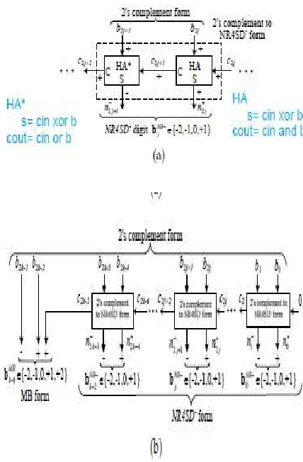
Figure 2: Block Diagram of the NR4SD− Encoding Scheme at the (a) Digit and (b) Word Level
Only four different values are used and not five as in MB algorithm, which leads to 0 ≤ j ≤ k − 2. As we need to cover the dynamic range of the 2’s complement form, the most significant digit is MB encoded (i.e., bMB
k−1 ∈ {−2,−1, 0, +1, +2}). The
Available online: https://edupediapublications.org/journals/index.php/IJR/ P a g e | 240
Figure 3: Block Diagram of the ) NR4SD+ Encoding Scheme at the (a) Digit and (b) Word Level
D.NR4SD− Algorithm
Step 1: Consider the initial values j = 0 and c0=0.
Step 2: Calculate the carry c2j+1 and the sum n+ 2j of a Half Adder (HA) with inputs b2j and c2j Fig. 2. c2j+1 = b2j ∧ c2j, n+ 2j = b2j ⊕ c2j.
Step 3: Calculate the positively signed carry c2j+2 (+) and the negatively signed sum n− 2j+1 (-) of a Half Adder* (HA*) with inputs b2j+1 (+) and c2j+1 (+) (Fig. 2). The outputs c2j+2 and n− 2j+1 of the HA* relate to its inputs as follows: 2c2j+2 − n− 2j+1 = b2j+1 + c2j+1.
Step 4: Calculate the value of the bNR
j− digit.
bNR−
j = −2n− 2j+1 + n+ 2j. (5)
Equation (5) results from the fact that n− 2j+1 is negatively signed and n+ 2j is positively signed.
Step 5: j: = j + 1.
Step 6: If (j < k−1), go to Step 2. If (j = k−1), encode the most significant digit based on the MB algorithm and considering the three consecutive bits to be b2k−1, b2k−2 and c2k−2. If (j = k), stop. Table 2
shows how the NR4SD− digits are formed.
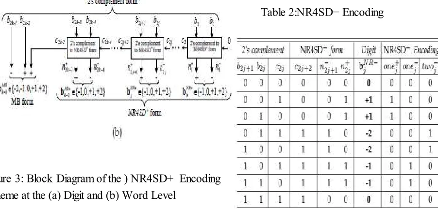
Table 2:NR4SD− Encoding
E.NR4SD+ Algorithm
Step 1: Consider the initial values j = 0 and c0=0.
Step 2: Calculate the carry positively signed c2j+1 (+) and the negatively signed sum n− 2j (-) of a HA* with inputs b2j (+) and c2j (+) (Fig. 3). The carry c2j+1 and the sum n− 2j of the HA* relate to its inputs as follows:
2c2j+1 − n− 2j = b2j + c2j.
The outputs of the HA* are analyzed at gate level in the following equations:
c2j+1 = b2j ∨ c2j, n− 2j = b2j ⊕ c2j.
Step 3: Calculate the carry c2j+2 and the sum n+ 2j+1 of a HA with inputs b2j+1 and c2j+1.
c2j+2 = b2j+1 ∧ c2j+1, n+ 2j+1 = b2j+1 ⊕ c2j+1.
Step 4: Calculate the value of the b NR-j digit.
W`bNR+
j = 2n+ 2j+1 − n− 2j. (7)
Equation (7) results from the fact that n+ 2j+1 is positively signed and n− 2j is negatively signed.
Available online: https://edupediapublications.org/journals/index.php/IJR/ P a g e | 241
Step 6: If (j < k−1), go to Step 2. If (j = k−1), encode the most significant digit according to MB algorithm and considering the three consecutive bits to be b2k−1, b2k−2 and c2k−2. If (j = k), stop. Table 3 shows how the NR4SD+ digits are formed.
Table3: NR4SD+ Encoding
The system architecture of the pre-encoded NR4SD multipliers is presented in Fig. 4. Two bits are now stored in ROM: n− 2j+1, n+ 2j (Table 2) for the NR4SD− or n+ 2j+1, n− 2j (Table 3) for the NR4SD+ form. In this way, we reduce the memory requirement to n+1 bits per coefficient [9]-[13] while the corresponding memory required for the pre-encoded MB scheme is 3n/2 bits per coefficient. Thus, the amount of stored bits is equal to that of the conventional MB design, except for the most significant digit that needs an extra bit as it is MB encoded.
Figure 4: System Architecture of the NR4SD Multipliers.
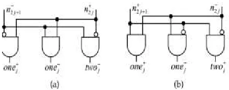
Figure 5: (a) NR4SD− and (b) NR4SD+ Encoding
Compared to the pre-encoded MB multiplier, where the MB encoding blocks is omitted, the pre-encoded NR4SD multipliers need extra hardware to generate the signals for the NR4SD− and NR4SD+ form, respectively. The NR4SD encoding blocks of Fig. 5 implements the circuitry of Fig. 4. And the Fig 6 shows the logical diagram of the PPG unit for existing design and fig 7 shows the proposed design of PPG unit.
After shaping the partial products, they are added, properly weighted, then adder to form the final result P=A.B in proposed system architecture, but in existing system, after shaping the partial products, they are added, properly weighted, through a Carry Save Adder(CSA). The CS output is given to the fast Carry Look Ahead (CLA) adder to get the final result.
The generation of the bit pj,i of the partial product
is illustrated at gate level in fig 5.
Available online: https://edupediapublications.org/journals/index.php/IJR/ P a g e | 242
Figure 7: Generation of the Bit pj,i of PPj in proposed design
The above diagram shows the generation of the bit in proposed design here using purely NAND [15] gates because these are universal gates. The existing system used AND gates, the transistor implementation count for AND was higher than the NAND gate so that replacing the AND to NAND gate in PPG unit for both positive and negative NR4SD.
IV. SIMULATION ANDRESULT
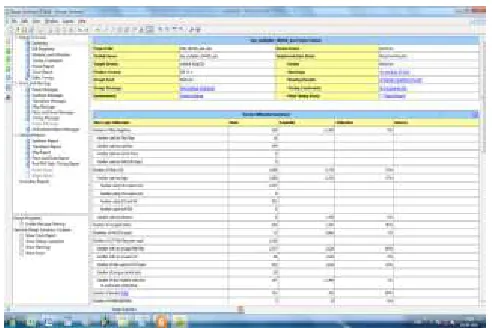
The simulate the proposed system architecture of Model sim and to analysis the area, power, and delay of the proposed system in Spartan 6 by using Xilinx software. The simulation result from the proposed NR4SD multiplier is shows in figure 8. The synthesis report on the proposed system is shown in figure 9 and figure 10. Finally the comparison of the proposed system is detailed in table I.
Fig.8: simulation result
Fig.9: synthesis report for NR4SD+
Table 4 tells about the comparison of two parameters power and delay. The power of the existing system of NR4SD+ is 27.50mw and NR4SD- is 26.40mw but the proposed system used 0.171w and 0.176w respectively. The power of the existing system of NR4SD+ is 2.29ns and NR4SD- is 2.28ns but the proposed system used 2.140ns and 2.142ns respectively.
Fig.10: synthesis report for
Table 4: comparison
Paramet er Exist ing sy st em Prop osed sy st em
NR4SD+ NR4SD - NR4SD+ NR4SD -
Power 27.50mw 26.40mW 0.171W 0.176W
Available online: https://edupediapublications.org/journals/index.php/IJR/ P a g e | 243
V.CONCLUSION
However this paper has had discussed about the architecture of pre-encoded multiplier were explored at offline the standard co efficient and storing them in system memory. The coefficient was used in non redundant radix 4 signed digits. The transistor implementation the count of the transistor for AND gate was higher than the NAND gate so that replacing the AND to NAND gate in PPG unit for both positive and negative NR4SD. This encoding technique was less complex partial product implementation and less area and more power efficient design. Analysis was verifying the proposed system was efficient from the existing system and the delay of the proposed system was 2.14ns.
REFERENCES
[1] K.Tsoumans, N.Axelos, N.Moshopoulos, G.Zervakis and K.Pekmestzi “ PRE-ENCODED MULTIPLIERS BASED On NON REDUNDANT RADIX 4 SIGNED DIGIT ENCODING”
[2] R.K. Kolagotla et al., ªVLSI Implementation of a 200-Mhz 16 16 Left-to-Right Carry-Free Multiplier in 0.35m CMOS Technology for Next-Generation DSPs,º Proc. IEEE 1997 Custom Integrated Circuits Conf., pp. 469-472, 1997.
[3] G. W. Reitwiesner, “Binary arithmetic,” Advances in Computers, vol. 1, pp. 231–308, 1960.
[4] K. K. Parhi, VLSI Digital Signal Processing Systems: Design and Implementation. John Wiley & Sons, 2007.
[5] K. Yong-Eun, C. Kyung-Ju, J.-G. Chung, and X. Huang, “Csdbased programmable multiplier design for predetermined coefficient groups,” IEICE Trans. Fundam. Electron. Commun.
Comput. Sci., vol. 93, no. 1, pp. 324–326, 2010.
[6] O. Macsorley, “High-speed arithmetic in binary computers,” Proc. IRE, vol. 49, no. 1, pp. 67–91, Jan. 1961.
[7] W.-C. Yeh and C.-W. Jen, “High-speed booth encoded parallel multiplier design,” IEEE Trans. Comput., vol. 49, no. 7, pp. 692– 701, Jul. 2000.
[8] Z. Huang, “High-level optimization techniques for low-power multiplier design,” Ph.D. dissertation, Department of Computer Science, University of California, Los Angeles, CA, 2003.
[9] Z. Huang and M. Ercegovac, “High-performance low-power left-to-right array multiplier design,” IEEE Trans. Comput., vol. 54, no. 3, pp. 272–283, Mar. 2005.
[10] Y.-E. Kim, K.-J. Cho, and J.-G. Chung, “Low power small area modified booth multiplier design for predetermined coefficients,” IEICE Trans. Fundam. Electron. Commun. Comput. Sci.,
vol. E90-A, no. 3, pp. 694–697, Mar. 2007.
[11] C. Wang, W.-S. Gan, C. C. Jong, and J. Luo, “A low-cost 256-point fft processor for portable speech and audio applications,” in Int. Symp. on Integrated Circuits (ISIC 2007), Sep. 2007, pp. 81– 84.
[12] A. Jacobson, D. Truong, and B. Baas, “The design of a reconfigurable continuous-flow mixed-radix fft processor,” in IEEE Int. Symp. on Circuits and Syst. (ISCAS 2009), May 2009, pp.
1133–1136.
Available online: https://edupediapublications.org/journals/index.php/IJR/ P a g e | 244
[14] M. Kolluru, “Audio decoder core constants rom optimization,” Patent US 6 108 633, Aug., 2000.
[15] H.-Y. Lin, Y.-C. Chao, C.-H. Chen, B.-D. Liu, and J.-F. Yang, “Combined 2-d transform and quantization architectures for h.264 video coders,” in IEEE Int. Symp. on Circuits and Syst.
(ISCAS 2005), vol. 2, May 2005, pp. 1802–1805.