A NEW METHOD TO AVOID CROWDING PHENOMENON IN EXTRACTING THE
PERMITTIVITY OF FERROELECTRIC THIN FILMS
Y. Wu, Z. Tang, Y. Xu, and X. He
School of Electronic Engineering
University of Electronic Science and Technology of China Chengdu, Sichuan 610054, China
Abstract—In this paper, a new method is proposed to avoid crowding phenomenon in extracting the permittivity of ferroelectric thin films. Polynomial curve fitting technique is used to determine the filling factor while the thickness of the thin film is very small. Conformal mapping (CM) combining with partial capacitance approach (PTA) is used to obtain the relationshipbetween the effective permittivity of multiplayer coplanar waveguide (CPW) and the permittivity of each layer. A CPW with a thin film layer is simulated and the permittivity of thin film is extracted, the results show that, by using the proposed method, the crowding phenomenon can be avoided successfully and the permittivity of thin films can be extracted accurately.
1. INTRODUCTION
by which the effective permittivity determined. Then, the filling factor of each layer can be calculated combining CM with PCA. At last, the relationshipbetween the effective permittivity of multiplayer CPW and the permittivity of each layer can be obtained. However, if the thickness of the thin film is very small, the results calculated directly by CM will lead to fail because of the crowding phenomenon [13].
In this paper, the polynomial curve fitting technique is used when the thickness of the thin film is less than a micron. By using this method, the crowding phenomenon can be avoided effectively. As the results shown, the permittivity of ferroelectric thin film can be extracted accurately, even the thickness of the film is only 500 nm and the width of the slot is 0.35 mm.
2. THEORY
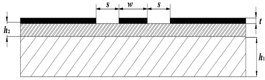
The structure of multiplayer CPW with ferroelectric thin film is shown as Figure 1. The widths of center conductor and slot are w and s
respectively, the thickness of the support layer is h1, the thickness of the thin film is h2, and the thickness of the conductor is t.
Figure 1. The structure of multiplayer CPW.
The effective permittivity can derived byS-parameters, as a b c d = 1 2
1−S112 S21
+S21
1 2
(1 +S11)2
S21 −
S21
1 2
(1−S11)2
S21 −
S21
1 2
1−S2
11
S21
+S21 (1)
and the normalized ABCD-matrix of the transmission-line is:
Comparing (1) and (2), the values ofγ can be obtained. Then the effective permittivity can be deduced as
εreff = (γ/γ0)2 (3) where
γ0 =j·2πf /c (4) and cis the velocity of light in vacuum.
In the other hand, by using PCA combining with CM, the effective permittivity can be expressed as [14]
εreff =q1·εr1+q2·εr2+ 1−q1−q2 (5) where εr1 and εr2 are relative permittivity of support layer (layer 1) and thin film respectively, andq1 and q2, which can be obtained from following formulations, are filling factors of support layer (layer 1) and thin film respectively.
q1 =
K(k1)
K(k1) −
K(k2)
K(k2)
2·K(k0)
K(k0)
(6)
q2 =
K(k2)
K(k2) 2·K(k0)
K(k0)
(7)
where
k0 =
w
2s+w (8)
k0 =
1−k2
0 (9)
k1 = sinh
πw h1+h2
sinh
π(2s+w)
h1+h2
(10)
k1 =
1−k2
k2 =
sinh
πw h2
sinh
π(2s+w)
h2
(12)
k2 =
1−k2
2 (13)
Then, the permittivity of thin film material can be derived as
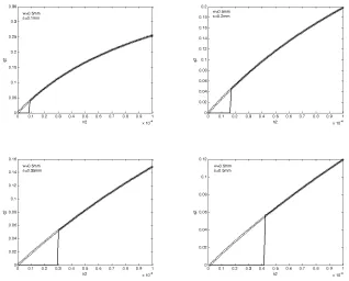
εr2 = (εreff −q1·εr1−1 +q1+q2)/q2 (14) From formulation (12) one can see that, if s, w h2, k2 becomes too small, which leads to numerical error in calculation elliptic function, that is the crowding phenomenon. To overcome the crowding phenomenon, the polynomial curve fitting technique is used in the region whichh2 is less than 100µm.
3. RESULTS
The filling factors of films with different thickness have been calculated, as shown in Figure 2, the solid lines are results by using elliptic functions and the circles are results by using polynomial curve fitting. Compared the two results in each figure one can see that, when the thickness of thin film is too small, the filling factor of thin film layer calculating by elliptic function falls dramatically, that may lead to numerical error, however, by using polynomial curve fitting techniques, the filling factor of thin films can be obtained accurately even the thickness of the thin films is very near to zero, in other words, the crowding phenomenon is avoided successfully.
0 2 4 6 8 10 12 14 16 18 0
500 1000 1500 2000 2500 3000
f (GHz)
p
e
rm
itti
v
ity
o
f th
in
fi
lm
m
a
te
ri
a
l
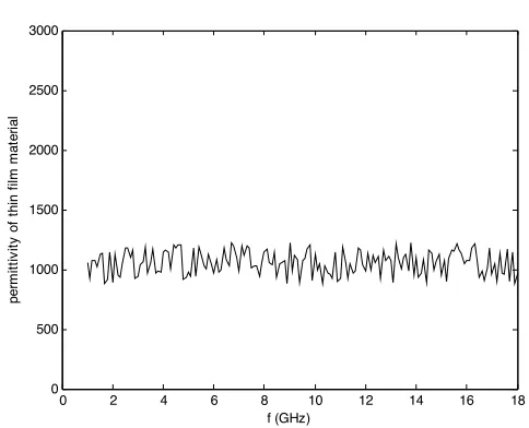
Figure 4. The extracting value of permittivity of the thin film material.
paper. As shown in Figure 4, comparing with the setting value of 1000, the permittivity of the thin film is extracted accurately.
4. CONCLUSION
In this paper, a new method to avoid crowding phenomenon in extracting the permittivity of thin film is proposed. Instead of calculating from ellipse function directly, the polynomial curve fitting technique is used to determine the filling factor when the thickness of the film is very small. Multilayer CPW constructers with different slot width and thin film thickness are investigated. Then a CPW with thin film of 500 nm is simulated and the permittivity of the film is extracted. As the result shown, by using the method proposed in this paper, the crowding phenomenon is overcome successfully and the permittivity of the thin film can be extracted accurately.
REFERENCES
2. Chou, Y.-H., M.-J. Jeng, Y.-H. Lee, and Y.-G. Jan, “Measurement of RF PCB dielectric properties and losses,” Progress In Electromagnetics Research Letters, Vol. 4, 139–148, 2008.
3. Challa, R. K., D. Kajfez, J. R. Gladden, A. Z. Elsherbeni, and V. Demir, “Permittivity measurement with a non-standard waveguide by using TRL calibration and fractional linear data fitting,” Progress In Electromagnetics Research B, Vol. 2, 1–13, 2008.
4. Eldek, A. A., “Wideband 180◦ phase shifter using microstrip-CPW-microstriptransition,” Progress In Electromagnetics Re-search B, Vol. 2, 177–187, 2008.
5. Yiddish, C., K. Gooney, M. Turkmen, and S. Kayak, “Neural models for coplanar strip line synthesis,” Progress In Electromagnetic Research, PIER 69, 127–144, 2007.
6. Kumar, A. V. P., V. Hamsakutty, J. Yohannan, and K. T. Mathew, “Microstripline fed cylindrical dielectric resonator antenna with a coplanar parasitic IC strip,” Progress In Electro-magnetics Research, PIER 60, 143–152, 2006.
7. Saed, M. A., “Reconfigurable broadband microstripantenna fed by a coplanar waveguide,”Progress In Electromagnetics Research, PIER 55, 227–239, 2005
8. Jiao, J.-J., G. Zhao, F.-S. hang, H.-W. Yuan, and Y.-C. Jiao, “A broadband CPW-FED T-shape slot antenna,” Progress In Electromagnetics Research, PIER 76, 237–242, 2007.
9. Si, L.-M. and X. Lv, “CPW-FED multi-band omni-directional pla-nar microstripantenna using composite metamaterial resonators for wireless communications,” Progress In Electromagnetics Re-search, PIER 83, 133–146, 2008.
10. Song, Y., Y.-C. Jiao, G. Zhao, and F.-S. Zhang, “Multiband CPW-FED triangle-shaped monopole antenna for wireless applications,” Progress In Electromagnetics Research, PIER 70, 329–336, 2007.
11. Liu, W.-C., “Optimal design of dualband CPW-FED G-shaped monopole antenna for WLAN application,” Progress In Electromagnetics Research, PIER 74, 21–38, 2007.
12. Nedil, M., M. A. Habib, T. A. Denidni, and H. Boutayeb, “Quasi-metallic-wall technique for increasing the efficiency of CB-CPW antennas,”Progress In Electromagnetics Research, PIER 78, 437– 455, 2008.