I I
II
9140
DIGITAL COMPUTER
GENERAL DESCRIPTION
Prepared By:
FOR PLANNING PURPOSES ONLY
SUBJECT TO CHA..N r,Ji! WITHOUT
NOTICE
(in
flr.J \,!/
ZZ
W\j~
Government Markeing PlanningSt. Paul, Minnesota
bL.
.~L.
E.
JOHNSON
nate:
September
17, 1964
I. INTRoDUCTION
9140 COMPUTER
GENERAL DESCRIPTION
The
9140
Computer is a general purpose, stored program, real-time digital processor. It usesbinar,y notation, is word organized, and operates with two's complement additive arithmetic. Input/output . data transfers are buffered, and the computer also includes acom-munications multiplexer interface for buffered operations with communications devices. All memory locations are directly addres-sable and may be used for storage of data or instructions.
9140 COMPUTER FE! TUBES
• 24 BIT WORD LENGTH, 8 BIT 'CHARACTER INSTRUCTIONS
• THREE FAST INDEX REGISTERS
• INDIRECT ADDRESSING
• AVERAGE INSTRUCTION TIME OF 1.2 MICROSECONDS
• 0.7'5 MICROSECOND MEMORY CYCLE TIME
o
BUFFERED I/O - OVER 3 MILLION CHARACTERS PER SECOND• BUFFERED COMMUNICATIONS I/O
• EXTERNAL AND INTERNAL PROGRAM INTERRUPI'S
• MEMORY PROTECTION FEATURE
e
OPTIONAL ARITHMETIC AND CONTROL UNITS-3-II. PHYSICAL CHARACTERISTICS
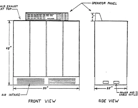
The 9140 Compu tar, including all logic, memory, inpu t/ou tpu t chan-nels, power supplies, and operator panel, is mounted in a single
cabine~ approximately 50 inches by 25 inches and
48
inches in height. Thus, the computer requires slightly over eight square feet of floor area. 'All wiring (power and peripheral data cables) may be brought out through the side of the cabinet at the floor level or through the bottom of the cabinet if the computer is to be used where a false floor ~s required or desired for other equipmants.Figure ,1 is a diagram of the 9140 Computer. The 9140 Computer uses forced 'room air for cooling and dissipates from 1,500 watts to 2,500 watts, depending upon the memory size, type of arithmetic and oontrol unit used, and the number of input/outp'\lt ohannels included. The front and rear doors of the computer cabinet are hinged at the sides and swing open to allow easy access to the blower, air filter, power
supply, 1ogic, and memory.
rhe operator panel is at a convenient height for use by an adult person, the center of the controls being approximately 51 inches from the floor. The operator panel indicators and controls are
display~d on a black background, and the center portion
or
the panel is rece,ssed slightly so that the neon indicators may be seen easily in high ambient light areas.AIR EXAUST AT T O P \
"\
I~
4
a"
\
FIGURE 1
9140 COMPUTER
~ OPERATOR PANEL
"T.:n
, i \
JL~
____________ _
I
~ 000 - 00. _ _ - QQO 000.HII~ ~
000000 000.00 _ 000 000 000 '0.' ' . ' f •• " , ... " ••
00. , ••••• '" .... .,.,. • . . . e.eo
I
I
_ .. -
-"-~ .... -... ~.
-
. ... ~ ... ""'... - "
.
r
~
.~
AIR INTAKE
50"
I
loooIIIicr-..-i.S II ...'_-,l ..
,. 1 ;a...tL-POWER ANO :r /0
CABLE OUTLETS
5
-III. FUNCTIONAL DESCRIPTION
The
914u
Computer has a minimum memor,r size of 8,192 - 24 bit words, expandable in 8,192 word increments to a maximum of 65,536 words. Figure'2 shows the relationships between word and eight bit char-acters in terms of the memory sizes offered.FIGY~ 2
MEMORY OPTIONS
Functional Unit Minimum Size Incremental Maximum Size
Size Offered ~ize Orfer§g Offered
24
bit word 8,192 8,19265,536
8 level character
24,576
24,576
196,608Memory modules may be added to an existing installation as a field modification.
Input/Output
The basic 9140 Computer con~ins as standard features, four input and four output (a tota.l of eight) ful.ly buffered general purpose high speed channelsJ each capable of transmitting up to
24
bits orthree; eight level charaoters irA parallel. The maximum input
Or
output "rate allowable with any peripheral device depends on system constraints auah as the number of peripheral devices which must operate' concurrently_ The maxtmum oomputer buf~ered data transfer rate, input B,nd output, can exceed one million 24 bit words per second or over three million sight level characters per second. Normally, with concurrent processing and
input/output,
the average data transfer rate will be much lower.The numbt..t' of. possible uuffer cont:!:oJ. ow'orda 18 not limited. by the number of input/output, channels. 'l'he basio 9140 Computer Input/ Output section contains fourteen addrftS8 lines such that oommunioa-tions type peripheral equipments may speoify the butfo~ oontrol word addresses to be used. This feature
per.mita
automatioBorting
and buffering of communications data between the9140 Oomputer
memorr
and
a larSG number
ot
communication. fac!11ti ••b1
U.Ior
tn.
UNIVAC Standard Communications SubsY8tem~Three additional sets of eight high spaed ohannels
(tour
for input
and
four for
output),eaoh set inoluding an additional ,roup
or .
address ,linea,
mar
be ordered as optional IQ,u1pment and oan beBuffered input/output word transfers may take one, two,' or three
memor,y cycles depending on how the transistor buffer control register& are assigned to I/O operations.
Instruo tion' Operation
The average instruction execution time of the 9140 .Computer depends on the ' individual program being run. The instruotion times, including all memory references normally vary from a minimum of 0.75
micro-second to a maximum or 2.25 mioroseoonds in the basic 9140 Prooessor. A.n'average of 1.2 microseconds per instruction may be expected with most programs..
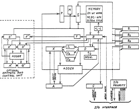
Figure 3 is a simplified block diagram of the 9140 Computer. The registers are identified b.Y capital letters. One of the optional arithmetic and control units is shovn in Figure 3. The operation of this optional unit is described in a separate manual. The following description of the functions of each of the registers will aid in understanding the operation of the basic
9140
Computer.Description of Registers
S - Stol-d.ge Address Register. The S Register is sixteen bits in length 'and is used to hold the address of the particular memory loca tion being accessed during the memory read!wri te cycle. This register is displayed on the operator panel and its contents may be manually altered except when the computer is operating at high speed.
,., .. \1 _ _ _ _ • T'I_+ ... '0 __ -' _+__ """,_,., 'O __ OC _+ __ .1/ ... + •• __ + ... .&'t_ •• _ 'I... .. .a._ J_
1:.1 - 1."I.'Qw.v~J Ala. ua. "'~5.L0 uo~ • ~"''''Q ~ "'~5.L0 UQJ. .Let UWQU UJ - 4 VI..&.J. V.L \10 .LU
length and, in general, is used to receive and hold the data read out of :the memory cell whose address is held in the S Register. The
Z,
or data register, is displayed on the operator panel and itscontents may be altered manually except when the computer is operating. at high speed.
X - Auxiliary .rlegister. The X Register is twenty-four bits in length' and is used as an auxiliary arithmetic register and data register. During adder operations, the contents of the
X
Register are auto-matically added to the contents of theD
Register.F - Function Register. The F Register is eight bits in length. It is used, to indicate the instruction being executed and it holds the operation or function code and instruction designators while they are being decoded and executed. The F Register is displayed on the operator panel to aid in program debugging.
C - Output Register. The C Register is twenty-four bits in length and is used to hold data which 1s to be transmitted to peripheral devices so that the computer can proceed with other operations simultaneously with the transmission of data to slower speed
r- - - ,- ,
I I
I ,
OPTIONAL.
ARITMSTIC ANt:) I
I ,. ... .,..0 .... ' 'UJI'" I
L ~ ~' • .:. ".-w: ..:':.- :.. ____ ..J
7
-FIGURE 3
TENTATIVE 9140 COMPUTER BLOCK DIAGRAM
ADDER
t-~
~I~
t
/
t
I
A
t1 EMORY
2.4 bit WORDS
4~ 81(,'" ('SK 0.7511$ c'teL
s
o..S
~!
"
I/O
8,
I
I
I/OI
l
PRloHlry
~I
~ ~~
,
J~' ~.... i
~I
!I ~
,
JL
II I
e~
'*Y"'*] /
A - Accumulator Register. The A Register is twenty-four bits in length. It is normally used to hold the results of arithmetic and logical operations between instructions" The A Register is explicitly addressable by most instruct,ions by setting Y = 1. The A Regilter is implioitly addressed and automatioally acoessed by those instructions which specify its use. The A Register is displayed on the operator panel as an aid for progrm debugging.
P - Program Address Register. The P Register is a sixteen bit register. The P Register holds the address of the next instruction to be executed and it may be explicitly addressed in most instructions by setting Y
=
O. The P Register is accessed automatically during , the operation of the computer for the purposes of incrementing and obtaining the addresses of instructions to be executed. The P Register is displayed on the operator panel.D - Auxiliary Arithmetic and Data Transfer Register. The twenty-four bit D Register is used to hold information presented to the adder. It is also used to transmit data to the index registers.
~, ~, BJ, B~ - Buffer Control Registers. Four twenty~four bit buffer control registers are provided outside of memory for use with ver,y fast peripheral devices. These registers hold the word counts arid/or data addresses during input/output operations. Core memor,y locations may also be used for buffer control word storage.
I1' I2,
,r, -
Index Registers. Three eighteen bit index registers are used to hold information which can be automatically added to the y portion of eaoh instruction before the instruction 1s executed. M - Memory Proteot Register. During the execution of instructions,the contents of the S Register ia compared to the contents
of
the S bit M,register. During instruction operations which alter the oontents of operand memory locations, the alteration is only allowed if the upper bits of the address falls within the range speoifiedbr
the contents of the M register. Where bits of M are set to ones, the porresponding upper bits ofS
must r~in invarientduring
operand memor,r write 01e18a.
Should
thevalue
inS
beoutside of
the range spec~.r1ed by' M, a MEMORY PROTECT INTERRUPr will oocur.
O'~her Fungtions
Other functions shown in the blook diagram inolude
the
input/outputpriority network,
~dder, and the memorr1norement1ng/dlcrsment1ng
logic.
Adder -
~eadder 1s a parallel, two'. oomplement twontr-tour bit
additive: unit
whichadds
twotwenty-tour 'bit number. (the oontent.
9
-Input/Output Priority - The I/O Priority network determines the next input/output function to be performed and in~~res that all requested I/O operations are noted and processed in an orderly manner.
Memory Inorementing/Deorementing Logie - An adder ds used between the memory read and write cycles during certain instructions which require 'a memory location to be incremented or decremented. This unit is also
used during input/output data transfers if me.mor,y contained 'buffer control words are accessed.
General TheorY' of Instruct:ton O'Rerat1on
T"ne accessing and execution of instrllctions are in tne form of suo-cessive sequences which are wired into the computer •. Each sequenoe normally involves a memor,y reference (read/write a.role), and the duration of a sequence normally coincides with the duration of the memory cycle •. '. The following deacript/1on applies to most of the
instructions.
Instructions begin with an A sequenoe. This sequenc$ inorements the contents of the P Register, extracts the instruction to be exeouted from memory, and restores the instruction in memory. During the last half of the A sequenoe, the funct:toll ordered by the instruotion is decoded along with the indirect and index register designators in the instruction. If the indirect designator is zero, certain
ot
the instructions may be completed during theA
sequence such &sLOAD,
CONSTANT,
JUMP,
SKIP, and someI/O
funotions. If the use ofan
index register ,is requirod, the oontents of the appropriate index register is added to ~he 1 portion of the instruction during the A sequence. If the i 'designator in the instruction is set to one, the next ___ •• A_~'" .t _ __ A .. _ _ ~ ... .a,.. •• +.c,...~ 4. +.", • .. ¥\AOC.,.." .... {T' •• "'"".,,,,,._'1""'''.
D0"i,",g44VV .4",,, VoL '""VoL .... ". ow""',.,"' .... v ... "" ... 1t ... y ... 1> .... ... ~ ... WI"''' .\ .... , ... "' __ ... _.. • .. __
sequenoe plaoes the fifteen bit address portion of the instruotion (or the address obtained in the index register modification) into the S Register. The data at this address is then read trom memory' and restored ;to memor,r. Thi! data become. the etfeotive operand addrell unless the b1na17 pos1 t10n ~.n this word oorresponding to the i de.i,-nator in this word 1s let to a one, the index modification and In-direct
(I)
aequence i . repoated according to the band 1 de.ignator settings in this new word. When the i designator il found to b, zero, the I sequencea terminate.The next sequence in the instruction ~cle il a I sequlnoe. It the contents of the accumulator are to b. placed at a stora,. looation,
the
Y sequenceis
used toplao.
this data at the addr ••• I. Itth,pro~ bal set
Y
=
1,
the contents of the Accumulator willb.
aoo •••• 4and a I •• quenoe will not be used. It thl oont.nt. ot a memcrT looa-tion are
to
be deoremented or inoremented, the operation11
perfor.m.4 b,r the incrementing/decrementing logicdurin,
the operand memor7 a.rola•In summary, the sequences are as follows:
A - Determines the address of the next instruction, calls the instruction from ~emory, and adds the index register contents to the instruction address to obtain the operand address. I • Uses the operand address to obtain the effective address of
the o'J)erand. This sequence may be repeated.
Y· Ex:tracts and/or modifies the operand.
l l
-IV. PROGRAMMING CHARACTERISTICS
The 9140 Computer instructions are twenty-tour l>1na17 digiti in length, a~d each instruction is contained in a single word in the computer memory. The instr~ctions consist of a six bit function code which defines the operation to be performed, a one bit indirect addressing designator, a two bit index register designator, and a fifteen bit operand address designator. Figure 4·shows the
instruc-tion word formato .
FIGURE
4
INSTRUCTION WORD FORMAT
r l
iI
bI
y23 18 17 16 15 14
o
r
=
function or operation code=
6 bits i=
indirect addressing designator=
1 bit b=
index register (one of three) designator=
2 bits1
=
oper~nd address designator=
15
bits9140
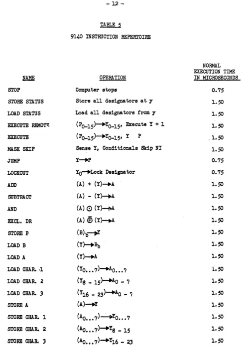
INSTRDCTIONREPERTOlRENORMAL EXECUTION TIME
NAME OPERATION, IN MICROSECOliDS
STOP Compu ter stops 0.7;
STORE STATUS Store all designators at 7 1.50
LOAD STATUS Load al~, designators from 7 1.50
EXECUTE RD10Tli: (PO-15)-"YO-15' Ex:ecute Y + 1 1. ;0
EXECUTE (PO-15)--'YO-l;'
I
p .1.50MASK SKIP Sense
I,
Conditionals' Skip NI 1. ;0JUMP Y--'P 0.75
LOCKOUT YO--.Lock Designator 0.75
ADD
(A)
+(Y)--.A
1. ;0SUBTRACT (A) - (YHA 1. ;0
AND (A)
0
(y)-t.A 1.;0EXCL. DR (A)
e
(YMA
1.;0STORE P
(B)b---tJ 1.;0LOAD B (YHBb 1.;0
LOAD!
(y)-.A
1.;0LOAD CHAR. ·1 (y 0 ••• 7 - . O ••• ? , ) A 'L.50
LOAD CHAR. 2
(IS -
15~AO
-
? 1. ;0LOAD CHAR. 3
(I16 - 23)--'AO -
? 1.50STORE A (1)-.y 1. SO
STORE CHAR. 1 'A)...:....Y \ 0 ••• 7 0 ••• 7 1.50
STORE CHAR. 2
(A.a •••
7)-+Y8 - lS 1.50NAME
INCREMENT
LOAD CONSTANT
INDEX SKIP
STORE ADDRESS
CHARA CTER SHIFT
SHIFT RIGHT
SHIFT LEFT
PARITY
ESCAPE*
ACTIVATE I/O
EXTERNAL FUNCTION STORE REMOTE
MEMORY PROTECT
13
-NORMAL
EXECUTION TIME
OPERATION
IN MICROSECONDS
(y) + l--+Y 1.60
Y ... A 0.75
(Y) - l-+Y, Skip NI if (Y) f
<
01.60
(AO•• .1;)-+YO ••• 15 1.50
(Y) Left Circular 8 bits 1.60
(A) Right open Y bits 0.75 + K (0.1)
(A) Left open Y bits
0.75
+ K(0.1)
Set designators 0.75
Define the instruction set and 0.75 optional arithmetic unit designated by Y
Activate Channel Y 0.75
(A)--.Channel y 0.75
ESI or Channel Y data--.A 0.75
Y~M O~75
The use of indirect addressing adds 0.75 microseconds to each instruction execution time per each indirect cycle executed. The use of the index registers does not add any additional instruction execution time~
*
The instruction repertoire for the 9140 Computer has been designed to allow ea8.1 programming of basic arithmetic, logical, and business decision operations. By storing each instruction in a 24 bit yord, optimum use of the storage tor instructions is realized, a. there are no wasted bit positions. The use of eight level characters for alpha and numeric information provides oompatibility vith all common computer character codes. The ability of the 9140 Computer to address characters in groups of three (three 8 level characters per word) provides ver,r fast operation. Note that certain instruc-tions are provided for operating on single characters in eaoh group of" three.
The 9140 Computer can directly address 32,768 words of storage and allow indirect addressing and indexing even with its short
instruc-tion. This ability makes software much easier to write, faster, and does not introduce a great nunfoer of programming restrictions.
Since all instructions are sho~t, and since the status of the designators may be stored and loaded with a single pair of instruc-tions, the handling of real-time interrupts' can be ~tremely rapid, and interrupts need not be deferred for long times. This allows
the 9140 Computer to handle real-time operations extremely fast. The basi6 9140 Computer instruction repertoire was designed using statistical IIfrequency of use" tables compiled from business, real-time, and information retrieval and storage programs in use on
various other computers. Single, double, and triple address computers were studied as well as decimal and binary types of machines. The 9140 Computer, for its functional size, represents an optimum
solu-tion for batch business, real-time, and informasolu-tion storage and retrieval problems. Instructions which are ver,y seldom used or needed may be programmed easily using the basic instructions
provided. For applications requiring extensive scientific computa-tion or multiword operacomputa-tions, the appropriate opcomputa-tional arithmetic and control unit may be added to the basic 9140 Computer to make an efficient application oriented processor.
Inpu t and ou tpu t
The basic 9140 Computer contains four general purpose high speed input channels and four general purpose high speed output channels. In addition, a set of address lines is provided for multiplexing a number of peripherals on to one of the high speed input and output channels. "
15
-The 9140 Computer memory and I/O logic also monitors and. controls the number of words to be transferred, the memory addresses involved,. and the oonditions under which the transfer of data is· automatically· stopped. No provisions need be made in the writing of programs for individual buffered I/O word transfers. thaT have no effect upon the program logic except to slav the running of the pro~ slightly and to interrupt the program after the proper number of words have been transferred.
The rate· of data word transfers between peripheral equipments and the 9140 Computer are governed by the transfer rate of the peripheral devices i f they are slower than the 9140 Computer and by the 9140 Computer if they are raster.
All of the 9140 input and output channels may be active concurrently. Through the use of the address lines provided and a communications . multiplexer, the number of active input and output data word buffers
is limited only by the number of peripheral devices which are required and the total data transfer rate which the 9140 Computer can handle from all of the peripheral devices combined.
Bn-rfer Control Warns
The 9140 Computer requires two twent,y-four bit words for each buffer operation to be established. These words are loaded initially by the program. They are then placed under oontrol of the input/output logic for the duration of the time during which the transfers will take place. The first word associated with a buffered transfer initially holds the count of the total number of data words to be transferred. The second word holds the address of the memory cell into which the first data word is to be placed (input), or the address of where the first output data vord is to be obtained from
(output). The word count is decremented and the data address is incremented automatically during each data transfer by the Input/ Output logic. When the count reaches zero, a monitor interrupt is generated.to inform the program that the number of words called for has been transferred. At the same time, the input/output logio also deactivates the channel. The procedure to initiate a buffered trans-fer of N; words is as follows z •
1. The program loads the count location for the desired ohannel with the number of words N.
2 The program loads the address location for the S~e channel with the first data storage address to be involved in the data ~ransfer.
3. The program executes an EXTERNAL FUNCTION. instruotion which
4.
The program executes an ACTIVATE I/O instruction which trans-fers control of the buffer control words to the input/output logicot
the channel involved. The actual transfer ofeta
t&words to or from the·9l40 Computer and the peripheral ·device then proceeds logically independent of the program.
When all of the words have been transferred, a monitor inter-·rupt will occur. This monitor interrupt will cause the computer
to execute an instruction in a memory looation permenently associated with the cbannelthrough:which the data transfers
took place. This has the effect of logically interrupting.the program. Interrupts may be locked out by use of the LOCKOUT instruction which is normally used only when transferring
c~ntrol fram one program to another under executive program control.
The buffered sequence for the transfer of a single word to or from the ~140 Computer and a peripheral device is as follows:
1. 2.
3.
5.
6.
The peripheral device sends the request to the computer. The computer suspends the execution of the next instruction temporarily for the next one, tW9, or three memory cycles. The count is read out of the buffer control word location and restored decremented. If the count restored is zero, the logic for generating a monitor interrupt is activated. The transfer, however, continues in either case.
The data address is read out of the second buffer word location and incremented. This data address, before incrementation, is
saved for .the data. memory cycle.
The data presented
b.1
the peripheral device is placed in memory at the data address (input), or the data at the address in memory is sent to the peripheral device (output). This data transfer cycle is the last operation in the buffered sequence.The program automatically resumes where it was suspended and the next instruction is executed, etc.
17
-given input channel, only one memory cycle is required per input 'Word transfer on that channel. If one B Register is assigned to
a
given channel, two memory C7cles will be required for a single data 'Wordt~ansfer on that channel, as the other bufter oontrol word used will
be in core memory. If none of the B Registers are assigned to a
given channel, a buffered word transfer will take three memory cycles, because both of the buffer control words will be in core memory.
The four B Registers may be assigned as desired among the four
Ilo
channels in the basic 9140 Computer as a factory option.Arithmetic and Control Unit Interface
The 9140 Computer is designed such that it may have additional processing power added to it in the form of optional arithmetic and control units. A generalized high speed logical interface is provided such that arithmetic and control units tailored for specific applica-tions may be used to optimize the processor for specific types of applica tiona.
For example, a multiword operation unit may be used to provide multi-word ed+ts, compare~ data moves, and BCD arithmetic. These operations may be Suspended temporarily when a real-time interrupt occurs with-out locking with-out interrupts for long periods of time or storing
VI. OPERA TOR PANEL,
The operator panel on the 9140 Computer i . us.d to
start
and,'topthe'
computer, enter a limited amount ot intormation,"displa,. the
contents
of an~memory location, aid in program debUgging, and facilitate' ,
maint,nance •. when it, is required.
The,lf1.yout
ot
the operator panel is" shown inrigure 6.
1000 000 000 eoo
'000 000 000 000 A
10 000 000 000 S
·0 000 000 000 P
FlGU~ 6
OPERATOR PANEL
000 0 0 0 0 0 0
0 0 0 000 000
.0OI~ @LOCI(
0001•
06Y;(JdUMP
0 @$I(IP
0Jt
3Po'.
000
o
0·01 c:~
.... ,I-a p(D!£RO
o 0 Olc:~ ~.
1000 000' f)~"
000 rea'
Power is applied to the 9140 Computerby' depressing the ON switoh. The switch lights when power is applied. If the OFF switch is ' depreased, the ON switch will become dark and power is removed. The procedure to start the 9140 Computer, high' speed, is as tollowss 1) With the camputeron, depress the CLEAR switch whic~
master
clears the computer. 2) Depress the HI SPEED switoh which readies the cQmputer for high speed operation. .3). Depress the LOAD switch •. Depre$sing the LOAD switch conditions the eampuer to accept a
pro-gr,am starting address. 4) Enter the starting addressot
the'program
into th~: P Register. If' a mistake is made, the register maY' be cleared
b.r
means or the smal~ clear butto~'to the right ottn. rells-ter. Finally, depress the RON switoh. Th, computer will indicat. a stopby
extinguishing theRUN
indicator .nd lightingthe
STOP
,indi ca tor.
In order to inspect any memo17 location
an4
enter data or instrue- ' tions' directly into the _ 9l40CoJDwter Mem0:t7, the CLEAR 'sw1 toh 8houl~ be depressed and the INSPECT switch shoul4 'bede~r.'8e4.19
-to be inspected should then be loaded into the Z Register. When The RON switch is depressedg the manually inserted address ~ll be
transferred to the S Register, and the information at that address in core memor,r vi1l be d11pla784 in the Z ReSister. ~i. information maY' be cleared out by means
or
the small clear bUtton t.o the right of the Z register, and new information maT be entered into this memory 100& tion b,y depressing the appropriate bit position indicatorswitches. .
lIn order to inspect the next consecutive address, the ADVANCE switch should be depressed. The oomputer will then automatically ,increment the address displayed in the S Register b,y one and will ·display ~e contents
or
this nev memo17 location i~ the Z Register ··It a different. address, not in sequence, is to be inspected, theSTOP, CLEAR, and LOAD awi tches should be depressed again. The new
address may then be ~tered into theS Register, and the computer maT be started as before.
Step operation allows slow speed operation
or
a program in such a way· that one instruction 18 executed each time that the ADVANCEswitch is depressed. The 9140 Computer should be placed into the 'STEP mode in order to operate at slow speed. This is aocomplished
by depressing the OLElR switch, followed
b7
deprelsing STEP sw1 tah.·The LOAD ew1tch should then be depresled, and the start1ng address
is entered: into the P Register. '!'he oomputer i l then started b;r depressing, the RUN awi tah. Each time, that the ADVANCE wi tah 11 depressed, the
9140
Computer will execute one instruotion. The Z Register and S lbgister will diapla,.the reeult.
ot
the last memory reference in the instruction jUlt executed. The f'unotion 004e will'\.. .... ~ .... _, ... _ .... A .t_ "'10. . . _ ... _ III ... _ .... A ... "' ... _ _ .. l1li+ ... ~ •. +-A ..
'IV· \,I. ... Dt'J.a3V\,l. J..u. 11649 &""",\jV,,"WU ~W."'IIiPVv .. , _&6\6 ., .... -~l' .. ,.,lI'.,-., • ... v . . . . . - _ •.
lettings will also be
displayed.
If peripheral device. are act! ve and &n I/O data transfer take. place following the instruction in the STEP mode, the la.t mamorT rererel\ce of' the input or output tranlt.r, data and &44%"1' will be dieplared in the Z and S :Register., re.pectively,
It' :thelW1tches on the Operator
l'anei
are not depressed 1%1 theoora
rect sequence, or it th-., are
depree.ad aoo1d.ntallf durins hi,h
lpeed operation, no harm will relUl tto
the electrical oomPOl'lct ••. 'same
ot
the program or data ltorecl inmemorr
maY
b. d •• tZ'07ed,how--ever', and it 11&7 be neOe81&rr to relol.d the mutilated information 81 ther auual17 or 'ria the boot.trap prtOlNlI and 4a
ta
.torecl in •peripheral ~.rloe suoh •• a cant r-.der.
!he tolll.owing inc1ioatorl, 111 aMit10n
to
the Z,. S, an4 .,!I,iatva
a~ d1eplared OIl the opera tor oODlole.
A .• the
a4
bit ao~toZ' NPIl1ia-tJP - indica tes if a jump instruction has been executed or 1£ the computer is conditioned to accept a starting address. SKIP - the skip indicator indicates if a skip instruction has been
executed, and the skip will be perfor.med.
FOS - the positive designator is set during certain instructions and is sensed by the SKIP instruction.
ZERO - the zero designator is set during certain instructions 'and is sensed by the SKIP instruction.
CAR - the carry designator is set during certain instructions when an adder carry occurs and it is sensed b,y use of the
SKIP instruction.
OVF ~ the overflow designator is set during certain arithmetic instructions when adder overflow oocurs. It is sensed by use of the SKIP instruction.
The neon indicators on the recessed portion of the Operator Panel andicate correctly only when the,y are set to one state over a long period of time or when the 'computer is in the INSPECT or STEP modes or when the compu ter is stopped. When the computer is operating at high speed, indications normally change at a rate too high for
the neon indicators or eye to follow, and any indications during high speed operation are normally not useful. Possible exceptions are operations where the computer is waiting most of the time and is operation very slow speed peripherals only.