and Programming System
for Parallel Signal Processing
David E. Van den Bout
Center for Communications and Signal Processing
Department of Electrical Computer Engineering
North Carolina State University
June 1987
Chapter 1. Introduction
...
1Chapter 2. Background 8
Chapter 3. My Thesis 46
Chapter 4. Algorithm Analysis 51
Chapter 5. Interprocessor Communications 69
Chapter 6. The DSP Architecture... 90
Chapter 7. The PaLS Automated Programming System 127
Chapter 8. Conclusions and Areas for Further Work... 220
References 238
Appendix A. The Axe Hardware Simulation Language... 248 Appendix B. Prediction of Simulated Annealing Curves for Graph Partitioning 278
lei Signal Processing (Under the direction ofT. K. MillerIII.)
This thesis describes an integrated assault upon the problem of designing high throughput, low cost digital signal processing systems. The dual prongs of this assault con-sist of:
• the design of a digital signal processor (DSP) which efficiently executes signal processing algorithms in either a uniprocessor or multiprocessor configuration,
• the PaLS programming system which accepts an arbitrary algorithm, partitions it across a group of DSPs, synthesizes an optimal communication link topology for the DSPs, and schedules the partitioned algorithm upon the DSPs.
The results of applying a newquasi-dynamic analysis technique to a set of high-level sig-nal processing algorithms were used to determine the uniprocessor features of the DSP design. For multiprocessing applications, the DSP contains an inierprocessor communications port(IPe) which supports simple, flexible, dataflow communications while allowing the total communication bandwidth to be incrementally allocated to achieve the best link utilization. The net result is a DSP with a simple architecture that is easy to program for both uniprocessor and multiprocessor modes of operation (as was verified using the newly developed hardware simulation language, Axe).
Introduction
The uses of signal processing are ubiquitous within our society, from the synthetic voice which reminds us to buckle our seatbelt to the enhanced pictures beamed to Earth from the Voyager spacecraft circling Jupiter. Before World War II, all signal processing was done in the analog domain (i.e. continuous-time, continuous-signal). With the advent of integrated circuits in the 1960's, many applications moved from the analog to the digital domain (i.e. discrete-time, quantized-signal). Digital techniques permit greater precision, repeatability, signal-to-noise ratio, and flexibility than their analog counterparts [AlleSS]. Programmable digital signal processors (DSPs) became widely available in the 1970's as large scale integra-tion (LSI) was introduced. Even greater flexibility is available to the user of these devices since their operation can be tailored merely by changing the signal processing program.
As usually happens, such benefits are offset by disadvantages. In the case of digital sig-nal processing, the bandwidth of the sigsig-nals which can be processed is much smaller than for analog techniques. Programmable DSPs can usually be applied to voice-frequency signals (~104 Hz) [Kawa80], while special-purpose digital systems can handle higher frequencies (::::106 Hz) [Lind85]. Analog systems have much higherthroughput, and can process signals of
ultra-high frequency (~1012Hz).
The operating physics of analog devices makes them faster for many common signal processing tasks. For example, determining the response y(t) of a linear system to a given inputx(t) is expressed mathematically as:
y
(t)=
f
h(t - a)x(a)d0:-ex;
where h(t) expresses the impulse response of the given analog system. This convolution
operation is a natural response of many types of analog systems. The digital form of
Eqn. (1.1) is:
N 1
Yk =
L
h,-~I X,1-0
(1.2)
where Yk' hk , and Xk are the discrete, digital counterparts of the previously described analog
signals. As can be seen, determining Yk for some value of k requires N multiplications and
N-1 additions. This digital form of convolution is not a natural operation of digital systems,
but must be explicitly provided for with hardware for performing multiplication and addition.
Special-purpose digital systems can use many adders and multipliers in parallel to compute
Eqn. (1.2), but to even approach the speed of analog convolution requires a large amount of
hardware. Programmable DSPs, which typically have only one multiplier, are much slower
than such hardware intensive systems.
The flexibility and programmability of digital systems also exacerbates their throughput
problem. New algorithms are being proposed which could not readily be performed with
analog components but are easily programmed on digital hardware. These algorithms (such as linear system solution and eigenvalue decomposition) require even greater computational
resources.
In order to expand the range of applicability of programmable DSPs, the speed at which
they execute signal processing algorithms must be increased. An increase in DSP speed can
be achieved by:
• increasing the speed of the circuit technology,
• creating signal processing algorithms with reduced computational requirements,
• enhancing the DSP architecture,
The speed and density of silicon technology has steadily increased over time, and new technologies such as gallium-arsenide are becoming commercially feasible [Milu86]. How-ever, quantum limits will eventually be reached beyond which further improvements are impossible [Mead80]. In any event, improvements in material technology can usually be
applied independently of the other speed-up methods mentioned. Therefore, the effects of improved technology will not be considered here.
Algorithms with reduced computational requirements (such as the Fast Fourier Transform (FFf) and Winograd FFf [Wino78]), can make digital signal processing practical for certain applications. However, these procedures are not easily discovered, nor do they pos-sess the usual simplicity of the majority of general-purpose signal processing algorithms. Therefore, this speed-up technique will not be expanded upon further.
Enhancing the architecture of a general-purpose computer in order to increase its perfor-mance for specific algorithms is a common technique. The execution speed of an algorithm can be increased as much as 10000/0 [Abd-74], although gains of 10%-50% are probably more common. In the same manner, the architecture of a programmable DSP canbealtered to effi-ciently support common digital signal processing operations. The architectural enhancements will usually consume some additional circuit area and power, and since these two quantities are not in unlimited supply, a careful costlbenefit analysis is needed. Still, this is a likely area in which to improve the performance of DSPs.
total system speed indefinitely, rather than just the 10%-500/0 performance improvement achieved from enhancing the architecture of a uniprocessor.
The appraisal of parallel processing given above is overly optimistic from a practical point of view. Typical parallel processing systems have saturated their performance at 2-3 times the speed of an individual processing component [Fish83]. Such systems are usually victims of communications bottlenecks. In effect, a significant portion of the system processing time is spent passing data between the individual computing elements. In the worst case, the time spent servicing this communication overhead cannot be used to perform useful computa-tions, thereby reducing the throughput of the system. Therefore, designers have spent con-siderable effort in developing parallel systems which minimize this overhead.
Probably the simplest multiprocessor network consists of a set of processing elements connected via a single global bus (Figure 1.1). The bus is used to transfer data and intermedi-ate results between processing elements. Because the bus can handle only one data transfer at a time, algorithm execution slows when multiple processors simultaneously attempt to transfer data. Thus, while a single global bus is simple and easy to implement, bus contention can decrease the total system throughput.
At the opposite extreme, a bus can connect each processing element (Figure 1.2). With
such a full interconnect, each processing element may transfer data without fear of conflicting
with another element. Unfortunately, the number of individual buses required for N
Global Bus
Figure 1.2: Multiple Processors with Complete Interconnect
processors is Ih(N2-N), which becomes unreasonably large (and costly) as N increases.
In order to reduce bus contention without building an extraordinary number of com-munication links, mesh-connected (Figure 1.3) and hyper-cube (Figure 1.4) multiprocessor networks have been built [Patt84]. These networks provide multiple buses (easing contention problems) but do not connect each pair of processing elements (lowering the implementation cost). A disadvantage of such networks is that data transferred from one processor to another may have to pass over several network links, thus increasing the transfer time (in the cases shown, the worst case delays are
a
(v'N )
anda
(log2N ), respectively).pe7
pe6
pel
peB
peS
pe2
pe9
pe4
pe3
Figure 1.3: Mesh-Connected Processing Elements
pe7
(~ ...---+----~
pe8
pe2
Figure 1.4:
" ( ~----t'-~
peS pe6
Hyper-Cube Processor Network
by the programmer and requires much time, effort, and knowledge of the underlying hardware architecture. Some headway has been made in automating this process for simple and/or regular multiprocessor architectures and algorithms such as those found in the realm of digital signal processing [Lin85].
To recap the high points of the previous discussion:
• Digital signal processing can be more widely applied by increasing the throughput of programmable DSPs.
• The throughput of a signal processing system can be increased by 1) optimizing the architecture of a DSP for commonly found signal processing operations, and 2) creating networks of these DSP elements to perform the algorithm in parallel.
• Circuitry constraints restrict the possible optimizations of a DSP. Circuitry considerations also limit the number of buses in a multiprocessor system, leading to communication bottlenecks which decrease the system performance.
• Even given a good DSP architecture and network, mapping algorithms to a multiprocessor is difficult.
CHAPTER
2
Background
1. Introduction
This chapter will survey several attempts by others to provide high-speed DSPs and
digital signal processing systems, along with software systems for mapping algorithms unto
such architectures. The various systems which will be examined are listed in Table 2.1.
2. Single-ChipDSPs
Single-chip digital signal processors usually operate stand-alone with no interaction with
a host computer. A typical system consistsof:
• a DSP chip,
Table 2.1: Digital Signal Processing Systems
Class Example Developer
RSP International Business Machines TMS320C25 Texas Instruments
Single-Chip DSPs ADSP-2100 Analog Devices DSP56000 Motorola DSP32 Western Electric J,LPD77230 NEC
Systolic Arrays PSC Carnegie-Mellon University WSAP University of Southern California
Array Processors MSSP Fairchild
MPP Goodyear Aerospace
Dataflow Systems ~PD7281 NEC
DFSP Helsinki University of Technology
lv1IMD Systems BRACELET North Carolina State University MUSEC AT&T
• some random access memory «64 Kbytes),
• an analog - digital converter (for acquiring input data from the environment), • and a digital - analog converter (for sending results to the environment).
Even these small systems possess sufficient resources to perform such tasks as digital filter-ing, adaptive equalization, echo cancellation, speech synthesis, etc. The architectural features which provide the necessary speed for such applications will be seen as each DSP is exam-ined.
2.1. Research Signal Processor (RSP)
The IBM Research Signal Processor architecture is shown in Figure 2.1 [Mint83]. Five functional subunits are discernible:
• Instruction fetch and sequence control unit, • Data store address generation unit,
• Data store access unit,
• Arithmetic and logic unit (ALU), • Input/output and control unit.
Instruction
J
StoreData
Store E
-Instruction Address
I
Address Data
,
,
Instruction Inst:- Inst.
~---=~Data Store ::: Fetch and .,. Address
Sequence Generation Addr.
Control
:::--Data Store Access
Inst.
-ALU
' J
I/O and Control RTC
--c_-=C-_~_f-.~{
_ _ _ __ . , _ - - - J
~
Control Scan
Interrupt
t
SPIO
t
Data
SPIO
1
The data store address generation and access units work in tandem to transfer data between the RSP and external memory. The address generator performs direct, offset, indexed, and masked addressing, permitting data memory to beaccessed in a very flexible manner. In particular, masked addressing allows the memory to be addressed with modulo-2" addresses. This supports the first-in/first-out (FIFO) data structures common in signal pro-cessing algorithms. The same registers which are used to form data addresses can also serve as loop counters, thus providing hardware support for iterative operations. Unfortunately, there is only one bus to the data memory. This bus can become a bottleneck during such operations as digital convolution, since two data values (hk -I and x,) must be fetched and multiplied.
The arithmetic logic unit inputs 16-bit fixed-point operands, but permits accumulation of sums up to 32-bits wide. This is necessary to preserve precision during calculations. The
ALU provides facilities for adding, subtracting, shifting, and logical functions. Interestingly, no hardware multiplier is provided. This function is performed in software using a special-ized shift instruction. The large size of the multiplier circuit and the presence of reduced computation algorithms (e.g. the Winograd FFr) were responsible for this design feature. As
was stated previously, such algorithms do not always exist for particular applications, so IBM has since developed DSPs with full hardware multipliers.
the first signal processing chips which operates in a stand-alone mode and also canbeused to build systems containing many RSPs.
Software support for the RSP includes a high-level assembler, linker/loader, simulator, debugger, and interface to the high-level language PUI. Nothing has been reported, how-ever, of automated tools for creating multiprocessor networks of RSPs.
2.2. The TMS320C25
The Texas Instruments TMS320C25 architecture (Figure 2.2) shares some similarities with the RSP [Fran86]. Both are built around a Harvard architecture with separate instruction
and data buses. Both work with 16-bit fixed-point integer values and accumulate 32-bit results. Like the RSP, the TMS320C25 can also be built into multiprocessing systems through the use of arbitrated global memory. Direct links between TMS320C25s are also possible using their built-in serial110 links, but the speed and flexibility of these links are limited.
Data Bus (16)
mux Shifter
PR (32) Multiplier
Data/Prog
256x16
Auxiliary Registers
Address
ALU
Data RAM
288x16
Program Bus (16)
Program ROM
4096x16
Stack
8x16
PC
Special Function Registers
Serial
I/O
In order to easily access operands as well as provide instructions with sufficient power to take advantage of the single instruction looping capability, the TMS320C25 contains a set of eight auxiliary registers which can be used as pointers to memory. These registers can be incremented or decremented (either by 1 or by the value stored in auxiliary register ARO) in parallel with the operations of the data ALU and multiplier, thus eliminating memory addressing delays and permitting fast processing of arrays of data. Bit-reversed addressing is
also provided to facilitate the programming of FFT routines. However, the TMS32OC2S does not possess an equivalent of the RSP masked addressing mode. Instead, the TMS320C25 sup-ports specialized instructions which simultaneously operate upon and move data in internal memory. These operations are useful for implementing general-purpose FIFOs since there is no restriction that the FIFO be of length 2" as in the RSP. The disadvantage of this technique is that, while the TMS320C25 readily handles short delay line FIFOs (such as are used in
biquad filter sections), each element of a long delay line must be individually moved. If no
cal-culations are performed on a significant portion of the FIFO elements, these lMS320C25 instructions are much less efficient than masked addressing.
The majority of programs for the lMS320C25 are coded in-line rather than using looping constructs and conditional branching. This is done to remove the overhead involved in doing the loop counter updates (for multiple instruction loops, only) and checking array boundaries. This coding technique creates lengthy programs which execute in minimum time since every operation performs a useful calculation. However, the length of the program can exceed the addressable program space of the TMS320C25 for some applications (e.g. 1024-point FFI). In these cases, instructions composing the outer program loops (which are not as time-critical) must berecoded as software controlled loops.
constructs into in-line code statements. There is no software provided to assist in program-ming multiprocessors built from severallMS320C25s.
2.3. The ADSP-2100
The architecture of the ADSP-2100 programmable signal processor is shown in Fig-ure 2.3 [Roes86]. Once again, a Harvard architectFig-ure is employed with separate instruction and data buses of widths 24 bits and 16 bits, respectively. A 14-bit address bus is paired with each data bus, allowing the ADSP-2100 to access up to 321<bytes of external memory.
Data computations are performed upon 16-bit fixed-point data using three separate arith-metic units: a general purpose 16-bit ALU, a shifter, and a 16x16 bit multiplier coupled with a
Data Address
ALU #1
Data Address
ALU #2
Cache Memory
Instr. Reg. Program Sequencer
Program Address Bus Data Address Bus
ALU
Instruction Bus Data Bus
Input Regs. Mult/Acc
2
Input Regs. Shifter
4O-bit accumulator (capable of performing 240 - 32=28= 256 multiplies and accumulations before
overflow occurs). These units operate in parallel and are connected by a local bus (the R bus) to avoid congestion of the main bus while passing intermediate results.
Delays in delivering operands to the arithmetic units are avoided by using two indepen-dent data address generators which support indexed, bit-reversed, and modulo addressing modes.
The absence of RAM within the ADSP-2100 requires the use of external memory for stor-ing data. Two operands are fetched by usstor-ing both the data and instruction buses and their associated address buses. Naturally, dual data accesses cannot be performed if the instruc-tion bus is being used to fetch the next instrucinstruc-tion. In order to reduce the congesinstruc-tion on the instruction bus, a cache containing the last 16 executed instructions is built into the ADSP-2100. Small program loops can be held within this cache, thus eliminating the need to fetch instructions from external memory. Of course, dual data fetches cannot be performed the first time through a program loop as the required instructions are not yet in the cache. Pro-gram execution speed increases on subsequent repetitions.
Multiprocessor systems composed of several ADSP-2100s can bebuilt by using the bus request and grant signals to manage access to a global memory. The ADSP-2100 also pro-vides a background register for each internal register to facilitate rapid storing and restoring of context. These features combine to support the creation of multiprocessors which are very responsive in the performance of mode changes.
Due to the complexity and flexibility of its operations, the ADSP-2100 is programmed using an algebraic code instead of instruction mnemonics. No support is available for pro-gramming multiprocessing systems built with the ADSP-2100.
2.4. The DSP56000
The DSP56000 (Figure 2.4) [Klok86] shares several features with the ADSP-2100 previ-ously presented:
• Instructions are 24-bits wide.
• Two independent address generators are provided for performing dual data fetches. Indexed, bit-reversed, and modulo addressing are all supported.
• Up to 15 nested, multi-instruction loops are supported in hardware using loop counter and end address stacks.
The DSP56000 also has significant differences from the ADSP-2100. First of all, the DSP56000 performs all data computations on 24-bit fixed point numbers rather than 16-bit data. This increases the dynamic range from 96 dB to 144 dB.
The single-cycle multiplier uses two 24-bit data values to generate 48-bil results. Accu-mutation of these results is done using 56-bit accumulators. As is in the ADSP-2100, the eight extra accumulator bits permit up to 256 multiply/accumulations to occur before overflow is
possible.
Address Bus Data Bus
,~
24/v
Bus Switch
[
Prog ra m
2048x24 [
X Memory
512x24 [ Ad d ressALU ]
YMemory ]
512x24
"
,
Data :;. Switch
Data ALU Mult.lAccum.
.~J
~. X Data /24 \
Int. YData / /24
Data ~- \
P
Data / /24 Switch «e-- Global 7 /24"
E - -
,
7V \
[
YO : [ ControllerProgramTI-
l ,~2// 3 )/
Clocks Interrupts
requiring the use of the instruction bus (as was done in the TMS320C25 and ADSP-21(0). Instructions or data may also beaccessed from external memory using the single set of exter-nal data and address buses.
There are several features which support multiprocessing in the DSP56000:
• Multiprocessors built around global memory are made possible by the inclusion of bus request and grant signals in the DSP56000 pinout. Such multiprocessors will require significant external hardware to manage the interface to the global memory.
• A DMA-like interface is provided which allows a host processor to control the operation of the DSP56000 as well as transfer data back and forth.
• A serial interface provides a slow, inexpensive link between multiple DSP56000s.
The DSP56000 is programmed using mnemonic assembly code. Standard development tools include an assembler, simulator, and a high-level language compiler. No support for programming multiprocessors is available.
2.5. The DSP32
The DSP32 (Figure 2.5) contains 5 primary subunits [Hays85]:
• a data arithmetic unit (DAU), • a control arithmetic unit (CAU), • several ROM and RAM memories, • a serial I/O unit (SID),
• a parallel I/O unit (PIO).
The DAU of the DSP32 represents its most dramatic departure from the previous
exam-pies. The DAU is capable of multiplying and adding 32-bit floating-point data values (24-bit
mantissa, 8-bit exponent) rather than fixed-point integers. This eliminates the need for
Floating Point Mult. Floating
Point Mult. Control
& Clocks
ROM RAM RAM
512x32 512x32 512x32
510
PIa
IJO (2)
b
, . . - - - f I / ' - - - a
Addr. (14) II Address Bus (16)
\ r - - - f f I\r-rr-~u'
1
( I/O (8)
DAU
simplified.
Because the DAV multiplier and adder are pipelined for maximum speed, it is difficult
to perform logic and control operations within this section. Instead, these functions are
han-dled in the CAV. The CAV is a full 16-bjt fixed-point computer which generates addresses
for the memory and controls the flow of execution in a signal processing program. Anyone
of 21 CAU registers may be used to address the data memory to obtain operands for the
DAV. The selected register is simultaneously modified by adding the contents of another
register to it. This operational sequence in combination with the CAU capability to perform
general computer type functions permits the synthesis of many flexible addressing modes.
The internal memory of the DSP32 contains enough ROM for a 512 instruction program,
as well as two RAM banks each capable of storing 512 floating-point numbers. The presence
of two RAM banks allows fast convolution as in the 1MS320C25. However, in the DSP32
these RAM banks form an interleaved ntel1lory systel11, so successive accesses to the same bank
leads to a decrease in performance due to increased memory waiting time.
The DSP32 l/O system contains a parallel port for use in passing data to and from a
host. There is also a serial interface which is primarily intended for interfacing to codecs, but
can provide a link in multiprocessor configurations (as in the 1MS320C25).
The DSP32 is programmed with sets of equations expressed in a 'C'<like syntax, much as
the ADSP-2100 is. Partitioning of programs to run on multiple DSP32s is done manually.
2.6. The ~PD77230
Like the DSP32, the JLPD77230 (Figure 2.6) operates upon 32-bit floating-point data
rather than fixed-point values [Eich86]. Other than this, however, the two processors are
RAMI
512x32
Multiplier t---. RAMO
512x32
Decoder Instruction
ROM
2048x32
EAU
12
Address Bus
--f-32
~~B~~~~~---~--~--~~~~~--~~--~--1
ALU
Two internal data RAMs are built into the J.LPD77230. These RAMs are non-interleaved, so their data may be accessed without excessive delays. Each RAM is also provided with an address generator which supports indexed and modulo addressing. (Bit-reversed addressing for FFT computations is performed using the main ALU.) Numerous internal buses exist to carry the data from theRAMs to where itis used. This prevents congestion of the main 32-bit data bus within the f-LPD77230.
The floating-point multiplier accepts two 32-bit values (24-bit mantissas and 8-bit exponents) and generates a 55-bit result (47-bit mantissa and 8-bit exponent). The associated floating-point ALU operates upon 47-bit fixed-point or 55-bit floating-point data and stores the result into a set of working registers. The ALU also contains a shifter which can be used to shift fixed-point data or can be driven by the exponent ALU so as to align floating-point values for addition or subtraction.
The f.LPD77230 instruction sequencer provides a single loop counter for hardware control of repetitive instructions. A bit in every instruction determines whether this counter will be
decremented or not. When the counter reaches zero, the following instruction is skipped and the loop is terminated. Thus, while the J.LPD77230 has hardware support for multiple instruc-tion loops, some software overhead is still necessary.
The f-LPD77230 can be used to create multiprocessors through the use of either its serial or parallel I/O ports. Low-speed, low-eost multiprocessors are obtained by cascading several f-LPD77230s via their serial ports. The parallel host interface may be used for higher speed systems.
3. Systolic Arrays
Systolic arrays [Kung79] attain high processing speeds by pipelining computations
within a regularly connected network of relatively simple processors. All communications
between processing elements are local and occur simultaneously as determined by a global
clock which controls the "beating" of the total system. The pipelining of systolic systems
pro-vides high speed while the short, regular interconnections simplify implementation.
How-ever, most proposals for systolic arrays entail systems dedicated to certain vector functions
(e.g. multiplying matrices). The expense of designing a system for such a narrow application
has hindered their implementation.
A natural solution to the cost problem is to develop programmable systolic array
ele-ments. The two examples described below represent slightly different attempts at this.
3.1. The Programmable Systolic Chip (PSC)
The Programmable Systolic Chip architecture (Figure 2.7) consists of 5 subunits
con-nected over a set of three buses:
• microinstruction storage and a sequencer,
• an ALU,
• a multiplier/accumulator (MAC),
• a set of three ports,
• and a register file.
User-defined horizontal microinstructions are stored in the microinstruction RAM.
Hor-izontal instructions allow the units of the PSC to be used in parallel to obtain minimal
execu-tion times for algorithms. The microsequencer is also able to perform multi-point branches
micro instruction
bus 1
bus 2
bus 3
Figure 2.7: PSC Architecture
The actual data manipulations occur in the ALU and MAC. Each of these units operates
on 9-bit operands: 8-bits of data and a L-bit tag which indicates some property of the data.
(The data word size limitation was brought about by technology limits at the time the PSC
was built.) The ALU and MAC contain logic and storage to simplify the programming of
multi-word operations (such as 32-bit arithmetic). The ability to operate these two units in
parallel as well as the natural pipelining of systolic systems allows high throughput systems
to be built with the PSC.
The register file stores operands for the ALU and MAC. Alternatively, operands may be fetched from another PSC through one of the three interprocessor ports. These three
two-way ports allow linear, hexagonal, and tree-like systolic structures to be implemented.
The PSC is programmed with a form of microassembly language. Formulation of
algo-rithms for systolic arrays will be discussed in a later section.
3.2. Wavefront Systolic ArrayProcessor (WSAP)
The Wavefront Systolic Array Processor (Figure 2.8) contains the same major
Upper Port
Instruction Memory
R
L Instruction Sequencer
e
f g
h
t -~
t P
P
0 Register ALU
File 0
r
r
Lower Port
Figure 2.8: The Wavefront Systolic Array Processor
The most significant alteration, however, concerns the philosophy of interprocessor communi-cation. All data transfers in standard systolic arrays occur simultaneously as directed by the global clock. Wavefront systolic arrays, however, pass data between elements as it becomes available in a dataflow type of protocol. This has several advantages:
• The systolic elements need no longer run in lock-step, Therefore, some sections of the array may be performing a different algorithm than other sections and true multi-processing can be achieved.
of results can be done without concern for the global timing scheme.
3.3. Systolic ArrayProgramming
Generating a systolic array which performs a given application requires the user to
specify the following:
• an interconnection pattern for the array elements;
• a timing format which insures that the correct data reaches the appropriate processors at the time it is needed;
• the computational steps performed by the individual array elements.
An algorithmic procedure has been developed for transforming the calculation intensive
inner loops of an algorithm into a systolic array [Mold83]. The method applies
transforma-tions to the data dependencies of a selected algorithm in order to derive a space and time
ord-ering.
In more detail, suppose the following nested loops were to be implemented as a systolic
array:
DO 10/1 = b1 toU 1
DO 10/2 = b2toU2
DO 10 /n = bn toun
5
1<!. )
52(1)
5N ( / )
10 CONTINUE
Here, / = {/1,J2, ... ,I"}is the set of loop indices and {SI,S2, ... ,SN}are the statements exe-cuted within the innermost loop. The set of all valid possible combinations of the loop
L"(/) =
{{It, .··
,I"}:bl~11~Ul,
.. ·b"~l"~un
}When the loop is executed, the elements of L" are lexicographically ordered by the manner in which the source code is written. This induced ordering can be modified to suit the algo-rithm for systolic arrays while maintaining the data dependencies for the assignment
state-Two indexed variables X/OJ) and Yg{iJ generated in statements 5(il ) and 5(i2), respec-tively, are data dependent if:
• X
tu,)
is an input variable to S(12)An algorithm has 'severaldata dependence vectors
d
=1
2 - 11,and the mapping procedureworks best if these are constant (as occurs in many signal processing algorithms). The set of dependence vectors imposes an ordering R on L". A transformation T is found which per-forms the following mapping:
T: <L",R
> -
<L¥,Rr>
where the data dependencies of the transformed set are selected by the user. If the user specifies a set of dependencies 6 for an algorithm with an original set of dependence vectors D, then the transformation is found from the set of diophantine equations:
TD = d
This transformation is guaranteed to exist if the user satisfies some restrictions on his choice of dependencies.
T
=
[~I
The
n
transformation governs the timing relationships of the systolic array, while S controls the spatial arrangement. It is desirable to minimize the dimensionality ofn
and maximize that of 5 since this will lead to maximum concurrency by replication of systolic array ele-ments.The structure of the individual systolic elements can be determined by applying similar transformations to the bit-level data dependencies of the individual statements.
The technique outlined above can map nested loops with constant data dependency vee-tors into a systolic array. A variation of the method allows a similar mapping into an array processor which supports global data transport between elements (this is precluded in systolic arrays). These methods are useful when applied to the most computationally intensive por-tion of signal processing algorithms, but do not address the problems involved in mapping the remaining, less-regular portions of the program.
4. ~ayProcessors
Array processors are typically composed of two major functional units:
• a one or two-dimensional array of simple processing elements which are usually connected in a nearest-neighborconfiguration;
• a standard computer which controls the operation of the processing array based upon commands it receives from a host computer.
All of the processing elements in the array perform the same operation in lock-step upon different pieces of data. Array processors are thus classified as single-instruction,
eliminates the need to synchronize inter-process communication - a major source of
commun-ication delays and performance degradation. Unlike systolic arrays, each processing element
has access to global data output by the control processor without having to ripple the data
through several communication links. Thus, array processors can attain the highest
throughput of any type of multiprocessor provided the application can be tailored to fit the
restrictive communication and flow-control capabilities of the array.
Two examples of array processors will be examined: a linear array for speech processing
and a mesh array for image enhancement.
4.1. Multi-Serial Signal Processor (MSSP)
The Multi-Serial Signal Processor (Figure2.9) is a one-dimensional array of simple pro-cessing elements intended for use in propro-cessing speech signals [Lyon84]. A central controller
is responsible for interfacing to the host computer and transferring data and instructions to
the linear array of processing elements. These array elements are connected in a
nearest-neighbor configuration so that data can only move left or right by one processor during an
HOST
Controller
64-word Multi-Port
RAM
Figure 2.9:
' - - - IALU
instruction cycle.
The Serial Signal Processing elements (SSPs) are each composed of 2 limiters, 2 adders, 2 multipliers, and an ALU which operate upon 32-bit signed data in a bit-serial manner. A 64-word RAM with the capability of delivering 8 words during an instruction is also provided. This combination of multiple arithmetic units and simultaneous access to multiple data words gives each processing element a high throughput rate.
The SSPs communicate with one another over I-bit wide serial links. Each element is provided with 5 input and 8 output links. While two input and output links per element would have been sufficient for a linear array, the extra communication paths are envisioned as being useful in implementing a tree-structured or two-dimensional processing system. All I/O between elements occurs in unison, thus eliminating the need for synchronization over-head and increasing throughput.
The processing elements do not have facilities for masking their operations or for indexed addressing of RAM data. A special ALU instruction is provided which can select between two data values based upon their sign, thus providing support for limiters, rectifiers, and conditional assignment. As for indexed addressing, this function is left to the array troller which determines the memory addresses accessed by the array elements. The con-troller itself is sparse in terms of its capabilities. No provision is made for looping constructs, so all loops are unrolledinto in-line code.
Programming the MSSP can be done with high-level languages which are translated to provide an intermediate sequential assignment code. This code is then processed by a com-piler which schedules the operations such that the correct results are produced in
near-optimal time while accounting for the pipeline delays of the SSP elements. The high-level
4.2. The Massively Parallel Processor (MPP)
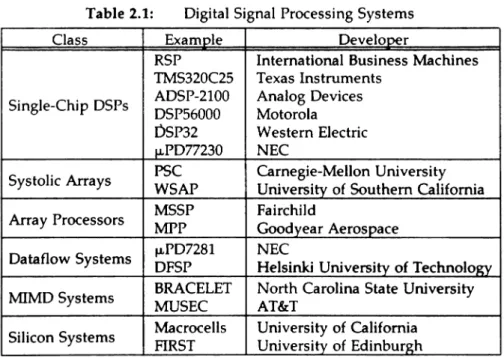
The Massively Parallel Processor is a two-dimensional array processor intended for pro-cessing image data from satellites [8atc80]. An array control unit is responsible for all non-parallel program operations and for managing an array consisting of 16,384 elements organ-ized into 128 columns of 128 processing elements each.
Due to the fact that many image processing algorithms operate upon L-blt wide data (pixels), the processing elements have simple I-bit wide data paths with a small amount of memory (Figure 2.10). Single-bit wide data paths exist between each element and its four neighbors. This allows the elements to combine the data they contain with that of their sur-rounding neighbors to enhance the quality of the image data. A L-bit adder and a I6-function logic unit are provided for this task. Each processor also has a mask register which can be
loaded and whose value will determine whether the associated element will participate in the next instruction.
left
-data bus
left right broadcast address
Special care was taken in the MPP to balance the VO and computational capabilities.
Each processing element contains a special register which allows it to shift data to its right neighbor while receiving data from its left neighbor. This facilitates the loading of new image data while processed data is being output. The MPP is also provided with a corner turning
nternorywhich formats the serial data from the satellite telemetry into two dimensional frames for the MPP array. These features insure that the processing array spend the majority of its time performing calculations instead of doingVO.
Due to the specialized application of the MPP and its simple processing elements, most coding is done by hand in order to obtain highly optimized code.
5. Dataflow Systems
Dataflow systems perform the computations specified by dataiiou: graphs. A dataflow graph specifies the data dependencies for a group of calculations (Figure 2.11). Operands (called tOkC71S) traverse the arcs of the graph and arrive at the inputs to the computational
a f
ab+cd+ef+gh
units. When a computational unit has at least one token upon every input, it fires, consuming the input tokens and producing an output token. This output token is passed along to any succeeding computational nodes in the graph, possibly causing some of them to fire. In some dataflow models, data tokens enter a queue at the computation unit inputs, while in others the computation nodes are not allowed to fire unless their output arcs are free of tokens. Thus, the computation is self-regulating so that data dependencies are not violated.
Typical data flow systems can be bisected into the following sections: Computation Section:
The calculations specified by the dataflow graph are executed by a set of processing elements. These elements may be as simple as those in systolic arrays and perform simple dyadic operations (small-grain datailoto), or they may be fully functional com-puters executing complex operations with many input tokens (large-grain dataflou'). Control Section:
A central controller schedules dataflow graph computations which possess all the necessary input tokens unto available processing elements. The central controller also collects the outputs from the computations and updates the inputs of any connected nodes.
Two dataflow implementations will be examined: a single-chip useful for building dataflow systems and a full dataflow signal processor.
5.1. The IiPD7281
The IiPD7281 is a single-chip dataflow element (Figure 2.12) intended to be used in image processing applications [NEC85]. Up to 14 of these chips may be arranged in a ring connected by 16-bit buses (Figure 2.13). The input controller within each fLPD7281 examines the tokens which circulate upon the interprocessor bus. If the address of a token matches the processor ID, the token is entered in the internal pipeline. Otherwise, it is passed along to the next processor through the output controller.
Flow Controller Processing
Unit Output
Queue
J_t'---r----l
Figure 2.12: A Block Diagram of the JLPD7281
PD7281
Dataflow Token Bus
The link tablestores the interconnection pattern for the part of the dataflow graph being executed by that particular processor. Using the link table, if the [unn controller determines that the incoming token has enabled the firing of a computational node, then the function table is accessed to retrieve the opcode which must be executed. The activated opcode, the new token, and any tokens previously stored in the data memoryare placed in the data queueto await manipulation by the processing unit. The sequence repeats using the output token from the processing unit to trigger any operations dependent upon the previously fired computa-tional node.
If the output from the processing unit does not trigger a node stored in the current pro-cessor, the address of the appropriate processor is appended to the token. The altered token is cycled through the pipeline to the output queueand is placed on the system bus by the out-put controller.
The ~PD7281 implements fine-grain dataflow and provides good throughput if its inter-nal pipeline can be kept full (7 tokens are needed for this). Many image processing applica-tions mesh naturally with its internal and interprocessor pipelining. Algorithms without such a regular communication structure would suffer from the rigid interconnection scheme.
Programming the JLPD7281 is done via assembly language. The user is required to manually break his program up between the the separate processing elements. Thus, while each f.LPD7281 dynamically determines parallelism present in its own piece of code during the execution of the algorithm, the user is required to specify the global concurrency.
5.2. The Data Flow Signal Processor (DFSP)
Bank of Processing
Elements
L DATA SECTION
Update Unit
Figure 2.14:
Activity Storage
The Data Flow Signal Processor
The operation of the DFSP is similar to that of the foLPD7281. An activity store holds the description of a dataflow graph along with information regarding the presence and absence of tokens upon the graph arcs. The fetch unit is triggered when a dataflow actor has sufficient input tokens to fire, and sends a description of the actor to an inactive member of thebank of processing elements. The fetch unit also triggers thedata transferunit such that the operands for
the actor are retrieved from data storage. These operands pass through the output DMA con-trollerand arrive at the triggered processing element.
Once the processing element has completed its assigned task, it signals the update unit which determines the correct destination for the generated result tokens. The result iransicr unit controls the storage of the results into the data storage block through the input DMA
have triggered any new actors. If so, it signals the fetch unit and the sequence begins again.
During operation, large blocks of data are typically passed to the processing elements of the DFSP. This is due to the complex operations performed by the dataflow actors, and the fact that processing elements receive copies of entire arrays rather than memory pointers. This causes congestion in the input and output DMA controllers. The coarse granularity of the dataflow operations can also reduce the available concurrency within a program.
Finer grained dataflow actors would allow more parallelism, but would also cause a bottleneck within the control section of the DFSP due to the increased rate of initiation and termination of the processing elements. Thus, while the DFSP frees the user from specifically identifying the parallelism within an algorithm, the need for the central controller to dynami-cally extract the concurrency can lead to decreased performance.
6. Multiple-Instruction Multiple-Data (MIMD) Systems
MIMD systems usually consist of a small number of processors of moderate to high complexity. Each processor runs its own program (multiple-instructions) on locally main-tained data (multiple-data) independently of the others until some resource (usually data) is needed from another processor. Then, the network interconnecting the processors is used to transfer the needed information. This requires some control overhead for identifying the requested information and synchronizing the transfer. This overhead reduces the throughput of MIMD systems and lessens their attractiveness for signal processing applications.
6.1. The BRACELET
The BRACELET system (Figure 2.15) is composed of the following components [MiIl86]:
• an array of 4 TMS32010 DSP chips connected via a network of 16-bit buses,
• a master controller which controls the array,
• a switch to channel I/O through the array,
• a global memory and bus to allow the TMS320s to access common data.
The TMS32010 DSP chips which make up the processor array can execute in synchrony
or they can diverge, run separate programs, and merge back into the SIMD mode. Thus, the
speed of array processors can be achieved while retaining the flexibility of MIMD machines.
The bus network connecting the four slave DSP chips is a combination of a ring and a
binary tree (this is more apparent on BRACELET networks with 8 or more slave processors).
The network was originally designed for the fast accumulation of inner products in adaptive
filtering algorithms, but can be used for general interprocessor communication, also. The
16-bit width of these buses permits fast transferral of data between processors, but also increases
the cost of implementation. For an N processor BRACELET, N log2N unidirectional buses are
needed. Since the TMS32010 provides no multiprocessing support, the networking circuitry
must all be provided externally, thus increasing cost and complexity.
The master controller transfers pipelined data in and out of the BRACELET array via the
switch. Data can bebroadcast to all the array processors through the global bus from either
the master processor or the global memory. This facilitates programming adaptive filters
where all the processors mustbeapprised of the error value after each iteration.
The BRACELET is programmed through a combination of TMS320 assembly language
and macro calls which support processor communication and other common functions. It is
archi-Global Bus (16)
J [
"'-..'/_'
TMS320
Slave #1 BRACELET Bus (16)
1MS320
Slave #2
Master
Controller Switch
\
Global Memory
TMS320
Slave #4
TMS320
Slave #3
'---_] L
.__
ltecture.
6.2. Multiplex Service Circuit (MUSEC)
The MUSEC system (Figure 2.16) is mainly intended as a testbed for parallel execution of speech processing algorithms [Knud84]. The system is used as follows:
Algorithm specification:
The user formats his algorithm as a high-level signal {lou' graph. This entails
partition-ing the task into a small set of relatively complex program modules. For example, an LPC speech processing application might be divided into modules for A-D conver-sion, pre-emphasis, windowing, autocorrelation, matrix solution, and FIR filtering. These program components pass processed signal values to one another during the execution of the algorithm.
Coding:
The detailed algorithm for each program module is coded in assembly for the AT&T DSP chip included in each Digital Signal Processing Module (DPSM). The
interconnec-tion of the modules is also specified.
Doumloading:
Each compiled program module is downloaded to a separate DSPM through the
Mas-ter Controller and the associated B-Bus. The inMas-terconnection list is loaded into the
Suiitd: Controller (SC) which sets up the initial configuration of DSPMs.
Algorithm execution:
Master ] Controller
Parallel B-Bus
DSPM
I---,Bt---,~
DSPM
sc
DSPM
DSPM
DSPM
links may be dynamically re-routed by the Switch Controller in response to a request from a DSPM. This permits a module to interface to two or more other modules.
The above system is simple and supports a model of communications similar to that of the actual application (i.e. signal flow graphs). The high-level modules do not permit max-imum concurrency, however, and the L-bit data links can create a communications bottleneck. Dynamic switching requests can also overload the switch controller.
7. Silicon Systems
A relatively recent method of creating signal processing systems is through the use of silicon compilers. Broadly stated, these compilers take as input a description of the algorithm and output the detailed schematic of an integrated circuit which executes the program. Sili-con systems designed by these compilers can attain very high processing speeds since they are constructed to run one specific algorithm. Such devices once built, however, cannot easily beused to perform other functions.
7.1. Macrocells
The Macrocell Compiler [Pope84] builds a signal processing system for a user specified algorithm as follows:
Manual partitioning:
The user manually divides the algorithm such that it can be run using several process-ing elements. A design file is created describing the particular program for each pro-cessing element as well as the interconnection network. The designer also specifies some hardware parameters for the processing elements, such as the word width of their accumulators and ALUs.
Global layout:
from the design file. A basic processor layout is then modified using this data in order to create specialized processors for each section of the partitioned program. The basic processor is composed of the following macrocclls:
• program counter • program storage • address generator • finite state machine • ALU with I/O ports • data storage
The size and presence of the above macrocells in the final system design is deter-mined by the extracted parameters.
Detailed layout:
Once the construction of each specialized processor is determined, the second pass of the compiler determines the detailed circuit layout for the entire system. The layout is determined by the size of the macrocells included in the processing elements as well as the processor interconnection network.
7.2. The FIRST Silicon Compiler
FIRST is a silicon compiler specialized for the creation of bit-serial signal processing sys-tems [Deny84]. The bit-serial approach slows the performance of arithmetic functions. This disadvantage is offset by the fact that bit-serial operations can be pipelined. The circuit ele-ments used for serial arithmetic are also easy to construct in a compacted form.
FIRST is used as follows:
Algorithm entry:
quite similar to a data f1owgraph, except the designer is required to synchronize data transfers between processing nodes by judiciously inserting delay elements. The designer can only use processing elements with direct hardware equivalents when constructing his flowgraph.
Circuit layout creation:
CHAPTER
3My
Thesis
1. The Problems of the Past
A significant percentage of signal processing systems are dedicated to performing one algorithm as fast and as cheaply as possible. The architectures examined in the previous sec-tion fail to provide such a service because they are lacking one or more of the following quali-ties:
Speed:
A system dedicated to a specific algorithm must be 1) built quickly, 2) programmed quickly, and 3) execute the program quickly.
Cost:
A signal processing system must have a low cost for dedicated applications. This depends on the availability of inexpensive components that are easily interconnected and programmed.
Flexibility:
Flexibility of the entiresystemis not so important for dedicated applications as is flexi-bility of the components used to build it. It must be possible to take the basic system component and use it to build substantially different systems without a large expendi-ture of time or money.
obtainable by using the serial ports on each DSP, but the communication delays are large and the serial ports do not allow enough connectivity in the network. Higher throughput can be
achieved by using a global memory multiprocessor architecture or by providing several fast, parallel buses between processing elements. This solution drives the implementation cost up due to the large amounts of external hardware needed to create the interfaces between the DSPs. Finally, mapping an algorithm to the completed network is a complex, manual pro-cedure dependent upon the topology of both the network and the algorithm data flow.
Systolic arrays and array processors attain very high speeds for select problems such as those with nested iterative loops. Some automated programming methodologies also exist for such algorithms. Irregular problems, however, do not map as well to these systems of regu-larly interconnected programmable elements, thus increasing the programming time and effort. The mapping is also complicated when the size of the algorithm exceeds the fixed size of the processing array. Increasing the size of the array is costly and inefficient if small prob-lems are being handled. In order to reduce the cost of array systems, the basic component must be built separately and interconnected as needed. However, the array processing ele-ments of many architectures (such as the MPP) are too simple to be generally applicable to a wide range of signal processing algorithms. The programmable systolic elements (PSC and WSAP) are a better choice, but their 110 schemes are too restrictive for many problems.
their automatic concurrency detection (e.g. the J.LPD7281) and re-introduced the mapping
problem.
MIMD systems lose much of their speed because of synchronization and communication
delays between the processing elements. Due to the expense of the interprocessor network,
the MIMD architectures produced so far have had fixed networks with low communication
delays averaged over many applications. These fixed networks are not optimal for all
algo-rithms, however, so some speed is given up for specific programs because it is too much
effort and costs too much to alter the topology. The resulting mismatch between the
algo-rithm and the architecture increases the mapping effort.
Dedicated signal processing systems created through the use of silicon compilers
achieve high sampling rates, but a new chip must be designed for every algorithm. This is
expensive for low-volume systems. There is also a relatively large time delay incurred by the
need to fabricate the system. Of course, a programmable system could be designed using a
silicon compiler, but this returns us to the question of how to construct a good programmable
signal processing system in the first place.
2. A Proposed Solution
Previously built signal processing architectures have not provided adequate solutions to
building high-speed, low-cost systems. My thesis is that such systems can be implemented if
the following are provided:
• a DSP chip with an architecture that efficiently executes the operations commonly found in signal processing software;
• an interprocessor communication scheme which efficiently handles the overhead involved in data transfers and permits the resources devoted to communications to be
incrementally allocated;
+
the topology for a network of the DSP elements,+ the partitioning of the algorithm for the network,
+
the scheduling of the algorithm components on the DSP elements, such that the execution time of the algorithm is minimized.Past attempts at computer design have taken the following directions:
• creation of a uniprocessor matched to a high-level language [Patt82], • creation of a uniprocessor and associated optimizing compiler [Henn82],
• and creation of a multiprocessor architecture and associated parallel compiler [Fish84].
My thesis takes the unique approach of designing a programmable DSP element which is easily built into a multiprocessor tailored for any specific digital signal processing algorithm. Each multiprocessing system will be synthesized by an automated design program working from the given signal processing algorithm. This is quite different from mapping an algo-rithm onto an already constructed multiprocessor network.
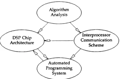
Figure 3.1 depicts the development process for the articles described above. A signal processing algorithm analysisis used to determine the uniprocessor qualities of the new DSP chip architecture. This insures a good match between the processor and the application area. Additional analysis will guide the choice of an intcrprocessor communication scheme. The method of transferring data between processors will affect the architecture of the DSP chip and the associated automated programming system. Once an initial configuration of the DSP chip and programming system are available, they will be iteratively modified to remove shortcomi ngs.
Algorithm Analysis
DSP Chip
Architecture } - - - t
Automated Programming
System
Interprocessor Communication
Scheme
CHAPTER
4Algorithm Analysis
1. Motivation
When designing a new computer, it is necessary to examine algorithms from the intended application area to find frequently used operations. Then the architecture of the proposed computer can be arranged to efficiently execute these operations. In this way, the computer architecture and application area are matched with the hope of improving some per-formance metric (e.g. throughput, memory usage, etc.),
This chapter describes the results of an analysis of a group of signal processing pro-grams. The analysis was performed to determine what characteristics a digital signal proces-sor should possess in order to efficiently execute such programs.
2. Plan Of Analysis
Previous efforts to analyze computer programs fall into two categories [Knut71] :
Static method:
The program text is scanned and statistics are kept concerning the relative frequency of the constructs and operations which are found. This method ignores the fact that some operations seldom occur in the program text but are executed many times while the program is running due to their inclusion within a loop or a much-used subrou-tine.
Dynamic
method:the significance of each operation is now based upon the actual number of times the operation is performed rather than how many times it occurs in the program text. A new problem arises, however, because the frequency of use for each operation may be dependent upon the data input to the program under analysis, and the statistics might change significantly from one data set to another. Such programs must be
analyzed several times with different data sets and the results merged into a final set of statistics.
The program analysis technique reported here uses a new method which is a combina-tion of the two discussed above. Since most signal processing algorithms use iterative loops which are nested within one another, a quasi-dunamic analysis method can be used. This entails automatically scanning the text of a program and adjusting a counter which records the current depth of loop nesting. Concurrently, as each program operation is encountered in the text, it is weighted by a factor dependent upon the current nesting depth and added into the statistical data. Obviously, those operations found within the innermost loop of a set of nested loops will weigh most heavily since they will be executed more often than those in the outer loops.
Quasi-dynamic analysis has the advantage of static analysis in that programs need only
3. The Signal Processing Program Set
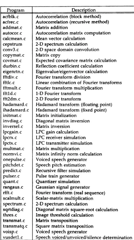
Once the method of gathering statistics is selected, a representative set of signal cessing programs is needed for analysis. The primary criteria for selecting such a set of pro-grams are:
• The programs must bewidely used in order to prevent the skewingof the statistics by some special-purpose algorithm.
• The major portion of each program must perform signal processing related operations. Program operations related to input and output of data are not desired since they are system dependent.
• The programs should be coded as efficiently as possible so that unnecessary and redundant operations do not affect the statistics.
• The programs must be written at as high a level as possible so that the use of signal processing operations is not affected by the underlying architecture of the target machine.
Table4.1: Signal Processing Programs Selected for Analysis
Program Description
acfblk.c Autocorrelation (block method) acfrec.c Autocorrelation (recursive method) addmat.c Matrix addition
autocor.c Autocorrelation matrix computation calcmean.c Mean vector calculation
cepstrum 2-D spectrum calculation conv3.c 2-D space domain convolution copymat.c Matrix copy
covmat.c Expected covariance matrix calculation durbin.c Reflection coefficient calculation eigenrtn.c Eigenvalue/eigenvector calculation fftdiv.c Fourier transform division
fftlc.c Linear combination of Fourier transforms fftmult.c Fourier transform multiplication
fft1d.c 1-D Fourier transform fft2dm.c 2-D Fourier transform
hadamard.c Hadamard transform (floating point) ihadamard.c Hadamard transform (fixed point) initmat.c Matrix initialization
invdiag.c Diagonal matrix inversion inversel.c Matrix inversion
Ipcgain.c LPC gain calculation lpcrx.c LPC receiver simulation lpctx.c LPC transmitter simulation multmat.c Matrix multiplication
normvi.c Matrix infinity norm calculation onepulse.c Voiced speech generator pitchdet.c Speech pitch estimation predict.c Recursive filter simulation pulser.c Pulse train generator quant.c Quantizer simulation rangaus.c Gaussian signal generator rfft.c Fourier transform (real sequence) scalmult.c Scalar-matrix multiplication spectrum.c 2-D spectrum calculation
sqrtdiag.c Diagonal matrix square-root calculation thres.c Image threshold calculation
transmat.c Matrixtransposition
transmatq.c Square matrix transposition
voisp.c Voiced speech generator
4. Results of the Program Set Analysis
Statistics in the following areas were gathered on the signal processing library:
• data variable usage, • arithmetic construct usage, • flow control usage,
• subroutine usage.
The subcategories of interest within each of these areas are given in Table 4.2.
4.1. Data Variable Usage
4.1.1. Static Analysis: Data Declarations
The relative frequencies of the various types of data variable declarations within the pro-gram set are given in Table 4.3.
As can beseen, global variables are infrequently used, accounting for -1% of the total number of data variable declarations. This is explained by noting that the programs in the set are intended to be used as subroutines, and the use of global data variables could cause unwanted side-effects. When global variables are used, they typically appear as floating-point arrays or as fixed or floating-floating-point scalars. Complex global data structures are not used.
Function arguments comprise -38% of all the data declarations. The bulk of the argu-ments are made up of integer scalars and floating-point arrays, although a significant
percen-tage of function arguments are pointers to customized data structures (-5%).
The remaining -60% of the data declarations are for local variables. The majority of the
Table 4.2: Statistical Categories for the Program Set
Catezorv Sub-Catezories Examples
Data global, local, int a.b.l,j, "c,ltd;
Variable and function float e,f,g[lO],h[lO], "m; Usage argument declarations struct complex x,y;
scalar references a = b + 5; array references ~[i] = h[i] + 5.0; pointer references "c = ltd + 5;
reference scope global, local, function argument Arithmetic bit-logical -, &, ', I,
»,
«
ConstructUsage logical &&, II,!
integer assignment a = b + 5;
integer arithmetic +,-,1,%, lifo,
++,-integer relations =,$,~,<,>
floating assignment e = f + 5.0; floating arithmetic +, _, I, It
floating relations -,$,~,<,>
Flow loopconstructs for, while, do
Control
Usage loop counter for(i=O; i<lO; i+ +) references ~[i]=h[i] +5.0; loop nesting for(i=O; i<lO; i+ +)
depth for(j=O; j<lO; j+ +)
....
conditionals if, 1:, switch, case
flow breaks break, goto, continue, return
Subroutine subroutine calls e = square_root(f); Usage
argument list length m
=
mat multtg.h): subroutineTable 4.3: Variable Declaration Percentages for the Program Set
Scalars Arrays
Scope Type
Absolute Pointer Absolute Pointer
Global int 0.17%
...
0.170/0.
...
(1.01%) float
...
.
...
0.67%...
double
...
.
...
.
...
.
...
struct...
.
...
.
...
...
other...
.
...
.
...
...
Function int 14.360/0 0.17% 0.33%
...
Arguments float 2.50% 0.67% 9.35%
...
(38.720/0 ) double 0.330/0
...
6.010/0...
struct
...
4.67%.
...
.
...
other...
0.330/0...
.
...
Local int 35.39%
...
0.33%...
(60.28%) float 13.86%
...
5.180/0...
double 1.840/0
...
0.67%...
struct 1.340/0 1.34%
...
.
...
other...
0.330/0.
...
.
...
The statistics given in Table 4.3 are purely static in nature and show only the frequency with which a particular data type is declared. No information regarding the frequency with which the variable is referenced during program execution is included. However, the follow-ing point is clear: the majority of data variables in the program set are simple integer and floating-point scalars and arrays. Some or all of the following factors may account for this:
• These data structures were the most natural for expressing the DSP algorithms.
• The programmer was very concerned with efficiency and knew that present-day computers handle simple data structures better than complex ones.
• The programmer did not understand the advantages gained by the use of more
complex data structures.
T